XMC4700 / XMC4800
Microcontroller Series
for Industrial Applications
XMC4000 Family
ARM® Cortex®-M4
32-bit processor core
Data Sheet
V1.1 2018-09
Microcontrollers
�Edition 2018-09
Published by
Infineon Technologies AG
81726 Munich, Germany
© 2018 Infineon Technologies AG
All Rights Reserved.
Legal Disclaimer
The information given in this document shall in no event be regarded as a guarantee of conditions or
characteristics. With respect to any examples or hints given herein, any typical values stated herein and/or any
information regarding the application of the device, Infineon Technologies hereby disclaims any and all warranties
and liabilities of any kind, including without limitation, warranties of non-infringement of intellectual property rights
of any third party.
Information
For further information on technology, delivery terms and conditions and prices, please contact the nearest
Infineon Technologies Office (www.infineon.com).
Warnings
Due to technical requirements, components may contain dangerous substances. For information on the types in
question, please contact the nearest Infineon Technologies Office.
Infineon Technologies components may be used in life-support devices or systems only with the express written
approval of Infineon Technologies, if a failure of such components can reasonably be expected to cause the failure
of that life-support device or system or to affect the safety or effectiveness of that device or system. Life support
devices or systems are intended to be implanted in the human body or to support and/or maintain and sustain
and/or protect human life. If they fail, it is reasonable to assume that the health of the user or other persons may
be endangered.
�XMC4700 / XMC4800
Microcontroller Series
for Industrial Applications
XMC4000 Family
ARM® Cortex®-M4
32-bit processor core
Data Sheet
V1.1 2018-09
Microcontrollers
�XMC4700 / XMC4800
XMC4000 Family
XMC4[78]00 Data Sheet
Revision History: V1.1 2018-09
Previous Versions:
V1.0 2016-01
V0.7 2015-10 (preliminary)
Page
Subjects
55
Added RMS Noise parameter in VADC Parameters table.
8
Corrected EtherCAT features to 8 Fieldbus Memory Management Units
(FMMU) and 8 Sync Manager.
46
Added footnote explaining minimum VBAT requirements to start the
hibernate domain and/or oscillation of a crystal on RTC_XTAL.
53
Added HIBIO characteristics.
59
Corrected DAC INL and gain error.
71
Changed frequency dependency of the current consumption.
74
Added peripheral idle current overview.
128ff
Updated package parameters and drawings.
133
Higher HBM and CDM ESD limits.
Trademarks
C166™, TriCore™, XMC™ and DAVE™ are trademarks of Infineon Technologies AG.
ARM®, ARM Powered®, Cortex®, Thumb® and AMBA® are registered trademarks of
ARM, Limited.
CoreSight™, ETM™, Embedded Trace Macrocell™ and Embedded Trace Buffer™ are
trademarks of ARM, Limited.
Synopsys™ is a trademark of Synopsys, Inc.
We Listen to Your Comments
Is there any information in this document that you feel is wrong, unclear or missing?
Your feedback will help us to continuously improve the quality of this document.
Please send your proposal (including a reference to this document) to:
mcdocu.comments@infineon.com
Data Sheet
V1.1, 2018-09
Subject to Agreement on the Use of Product Information
�XMC4700 / XMC4800
XMC4000 Family
Table of Contents
Table of Contents
1
1.1
1.2
1.3
1.4
1.5
Summary of Features . . . . . . . . . . . . . . . . . . . . . . . . . . . . . . . . . . . . . . . . 8
Ordering Information . . . . . . . . . . . . . . . . . . . . . . . . . . . . . . . . . . . . . . . . . 10
Device Types . . . . . . . . . . . . . . . . . . . . . . . . . . . . . . . . . . . . . . . . . . . . . . . 10
Device Type Features . . . . . . . . . . . . . . . . . . . . . . . . . . . . . . . . . . . . . . . . 11
Definition of Feature Variants . . . . . . . . . . . . . . . . . . . . . . . . . . . . . . . . . . 13
Identification Registers . . . . . . . . . . . . . . . . . . . . . . . . . . . . . . . . . . . . . . . 14
2
2.1
2.2
2.2.1
2.2.2
2.2.2.1
2.3
General Device Information . . . . . . . . . . . . . . . . . . . . . . . . . . . . . . . . . .
Logic Symbols . . . . . . . . . . . . . . . . . . . . . . . . . . . . . . . . . . . . . . . . . . . . . .
Pin Configuration and Definition . . . . . . . . . . . . . . . . . . . . . . . . . . . . . . . . .
Package Pin Summary . . . . . . . . . . . . . . . . . . . . . . . . . . . . . . . . . . . . .
Port I/O Functions . . . . . . . . . . . . . . . . . . . . . . . . . . . . . . . . . . . . . . . . .
Port I/O Function Table . . . . . . . . . . . . . . . . . . . . . . . . . . . . . . . . . . .
Power Connection Scheme . . . . . . . . . . . . . . . . . . . . . . . . . . . . . . . . . . . .
15
15
18
21
29
30
38
3
3.1
3.1.1
3.1.2
3.1.3
3.1.4
3.1.5
3.2
3.2.1
3.2.2
3.2.3
3.2.4
3.2.5
3.2.6
3.2.7
3.2.8
3.2.9
3.3
3.3.1
3.3.2
3.3.3
3.3.4
3.3.5
3.3.6
3.3.7
3.3.8
3.3.9
Electrical Parameters . . . . . . . . . . . . . . . . . . . . . . . . . . . . . . . . . . . . . . .
General Parameters . . . . . . . . . . . . . . . . . . . . . . . . . . . . . . . . . . . . . . . . .
Parameter Interpretation . . . . . . . . . . . . . . . . . . . . . . . . . . . . . . . . . . . .
Absolute Maximum Ratings . . . . . . . . . . . . . . . . . . . . . . . . . . . . . . . . . .
Pin Reliability in Overload . . . . . . . . . . . . . . . . . . . . . . . . . . . . . . . . . . .
Pad Driver and Pad Classes Summary . . . . . . . . . . . . . . . . . . . . . . . . .
Operating Conditions . . . . . . . . . . . . . . . . . . . . . . . . . . . . . . . . . . . . . . .
DC Parameters . . . . . . . . . . . . . . . . . . . . . . . . . . . . . . . . . . . . . . . . . . . . .
Input/Output Pins . . . . . . . . . . . . . . . . . . . . . . . . . . . . . . . . . . . . . . . . . .
Analog to Digital Converters (VADC) . . . . . . . . . . . . . . . . . . . . . . . . . . .
Digital to Analog Converters (DAC) . . . . . . . . . . . . . . . . . . . . . . . . . . . .
Out-of-Range Comparator (ORC) . . . . . . . . . . . . . . . . . . . . . . . . . . . . .
Die Temperature Sensor . . . . . . . . . . . . . . . . . . . . . . . . . . . . . . . . . . . .
USB OTG Interface DC Characteristics . . . . . . . . . . . . . . . . . . . . . . . . .
Oscillator Pins . . . . . . . . . . . . . . . . . . . . . . . . . . . . . . . . . . . . . . . . . . . .
Power Supply Current . . . . . . . . . . . . . . . . . . . . . . . . . . . . . . . . . . . . . .
Flash Memory Parameters . . . . . . . . . . . . . . . . . . . . . . . . . . . . . . . . . .
AC Parameters . . . . . . . . . . . . . . . . . . . . . . . . . . . . . . . . . . . . . . . . . . . . .
Testing Waveforms . . . . . . . . . . . . . . . . . . . . . . . . . . . . . . . . . . . . . . . .
Power-Up and Supply Monitoring . . . . . . . . . . . . . . . . . . . . . . . . . . . . .
Power Sequencing . . . . . . . . . . . . . . . . . . . . . . . . . . . . . . . . . . . . . . . . .
Phase Locked Loop (PLL) Characteristics . . . . . . . . . . . . . . . . . . . . . .
Internal Clock Source Characteristics . . . . . . . . . . . . . . . . . . . . . . . . . .
JTAG Interface Timing . . . . . . . . . . . . . . . . . . . . . . . . . . . . . . . . . . . . . .
Serial Wire Debug Port (SW-DP) Timing . . . . . . . . . . . . . . . . . . . . . . . .
Embedded Trace Macro Cell (ETM) Timing . . . . . . . . . . . . . . . . . . . . .
Peripheral Timing . . . . . . . . . . . . . . . . . . . . . . . . . . . . . . . . . . . . . . . . . .
40
40
40
41
42
45
46
47
47
54
58
62
64
65
67
71
75
77
77
78
79
81
82
84
86
87
88
Data Sheet
5
V1.1, 2018-09
Subject to Agreement on the Use of Product Information
�XMC4700 / XMC4800
XMC4000 Family
Table of Contents
3.3.9.1
3.3.9.2
3.3.9.3
3.3.9.4
3.3.9.5
3.3.10
3.3.10.1
3.3.10.2
3.3.10.3
3.3.10.4
3.3.11
3.3.12
3.3.12.1
3.3.12.2
3.3.12.3
3.3.12.4
3.3.13
3.3.13.1
3.3.13.2
3.3.13.3
3.3.13.4
3.3.13.5
Delta-Sigma Demodulator Digital Interface Timing . . . . . . . . . . . . . . 88
Synchronous Serial Interface (USIC SSC) Timing . . . . . . . . . . . . . . 89
Inter-IC (IIC) Interface Timing . . . . . . . . . . . . . . . . . . . . . . . . . . . . . . 92
Inter-IC Sound (IIS) Interface Timing . . . . . . . . . . . . . . . . . . . . . . . . . 94
SDMMC Interface Timing . . . . . . . . . . . . . . . . . . . . . . . . . . . . . . . . . 96
EBU Timing . . . . . . . . . . . . . . . . . . . . . . . . . . . . . . . . . . . . . . . . . . . . . 104
EBU Asynchronous Timing . . . . . . . . . . . . . . . . . . . . . . . . . . . . . . . 104
EBU Burst Mode Access Timing . . . . . . . . . . . . . . . . . . . . . . . . . . . 111
EBU Arbitration Signal Timing . . . . . . . . . . . . . . . . . . . . . . . . . . . . . 113
EBU SDRAM Access Timing . . . . . . . . . . . . . . . . . . . . . . . . . . . . . . 114
USB Interface Characteristics . . . . . . . . . . . . . . . . . . . . . . . . . . . . . . . 118
Ethernet Interface (ETH) Characteristics . . . . . . . . . . . . . . . . . . . . . . . 119
ETH Measurement Reference Points . . . . . . . . . . . . . . . . . . . . . . . 119
ETH Management Signal Parameters (ETH_MDC, ETH_MDIO) . . 120
ETH MII Parameters . . . . . . . . . . . . . . . . . . . . . . . . . . . . . . . . . . . . 121
ETH RMII Parameters . . . . . . . . . . . . . . . . . . . . . . . . . . . . . . . . . . . 122
EtherCAT (ECAT) Characteristics . . . . . . . . . . . . . . . . . . . . . . . . . . . . 123
ECAT Measurement Reference Points . . . . . . . . . . . . . . . . . . . . . . 123
ETH Management Signal Parameters (MCLK, MDIO) . . . . . . . . . . 123
MII Timing TX Characteristics . . . . . . . . . . . . . . . . . . . . . . . . . . . . . 124
MII Timing RX Characteristics . . . . . . . . . . . . . . . . . . . . . . . . . . . . . 126
Sync/Latch Timings . . . . . . . . . . . . . . . . . . . . . . . . . . . . . . . . . . . . . 127
4
4.1
4.1.1
4.2
Package and Reliability . . . . . . . . . . . . . . . . . . . . . . . . . . . . . . . . . . . . .
Package Parameters . . . . . . . . . . . . . . . . . . . . . . . . . . . . . . . . . . . . . . . .
Thermal Considerations . . . . . . . . . . . . . . . . . . . . . . . . . . . . . . . . . . . .
Package Outlines . . . . . . . . . . . . . . . . . . . . . . . . . . . . . . . . . . . . . . . . . . .
5
Quality Declarations . . . . . . . . . . . . . . . . . . . . . . . . . . . . . . . . . . . . . . . 133
Data Sheet
6
128
128
128
129
V1.1, 2018-09
Subject to Agreement on the Use of Product Information
�XMC4700 / XMC4800
XMC4000 Family
About this Document
About this Document
This Data Sheet is addressed to embedded hardware and software developers. It
provides the reader with detailed descriptions about the ordering designations, available
features, electrical and physical characteristics of the XMC4[78]00 series devices.
The document describes the characteristics of a superset of the XMC4[78]00 series
devices. For simplicity, the various device types are referred to by the collective term
XMC4[78]00 throughout this manual.
XMC4000 Family User Documentation
The set of user documentation includes:
•
•
•
Reference Manual
– decribes the functionality of the superset of devices.
Data Sheets
– list the complete ordering designations, available features and electrical
characteristics of derivative devices.
Errata Sheets
– list deviations from the specifications given in the related Reference Manual or
Data Sheets. Errata Sheets are provided for the superset of devices.
Attention: Please consult all parts of the documentation set to attain consolidated
knowledge about your device.
Application related guidance is provided by Users Guides and Application Notes.
Please refer to http://www.infineon.com/xmc4000 to get access to the latest versions
of those documents.
Data Sheet
7
V1.1, 2018-09
Subject to Agreement on the Use of Product Information
�XMC4700 / XMC4800
XMC4000 Family
Summary of Features
1
Summary of Features
The XMC4[78]00 devices are members of the XMC4000 Family of microcontrollers
based on the ARM Cortex-M4 processor core. The XMC4000 is a family of high
performance and energy efficient microcontrollers optimized for Industrial Connectivity,
Industrial Control, Power Conversion, Sense & Control.
EtherCAT
System
Masters
System
Slaves
SCU
CPU
RTC
ARM Cortex-M4
ERU0
GPDMA0
System
DCode
GPDMA1
Ethernet
WDT
USB
OTG
ICode
FCE
Bus Matrix
Data
Code
PSRAM
PMU
ROM & Flash
USIC0
DSD
PBA0
CCU80
CCU81
DSRAM2
LEDTS0
CCU43
VADC
POSIF0
EBU
PORTS
DAC
PBA1
Peripherals 1
Peripherals 0
ERU1
Figure 1
POSIF1
DSRAM1
CCU40
CCU41
CCU42
SDMMC
USIC2
USIC1
MultiCAN
System Block Diagram
CPU Subsystem
•
•
•
•
•
•
•
CPU Core
– High Performance 32-bit ARM Cortex-M4 CPU
– 16-bit and 32-bit Thumb2 instruction set
– DSP/MAC instructions
– System timer (SysTick) for Operating System support
Floating Point Unit
Memory Protection Unit
Nested Vectored Interrupt Controller
General Purpose DMA with up-to 12 channels
Event Request Unit (ERU) for programmable processing of external and internal
service requests
Flexible CRC Engine (FCE) for multiple bit error detection
Data Sheet
8
V1.1, 2018-09
Subject to Agreement on the Use of Product Information
�XMC4700 / XMC4800
XMC4000 Family
Summary of Features
On-Chip Memories
•
•
•
•
•
16 KB on-chip boot ROM
96 KB on-chip high-speed program memory
128 KB on-chip high speed data memory
128 KB on-chip high-speed communication memory
2,048 KB on-chip Flash Memory with 8 KB instruction cache
Communication Peripherals
•
•
•
•
•
•
•
•
Ethernet MAC module capable of 10/100 Mbit/s transfer rates
EtherCATSlave interface (ECAT) capable of 100 Mbit/s transfer rates with 2 MII
ports, 8 Fieldbus Memory Management Units (FMMU), 8 Sync Manager, 64 bit
distributed clocks
Universal Serial Bus, USB 2.0 host, Full-Speed OTG, with integrated PHY
Controller Area Network interface (MultiCAN), Full-CAN/Basic-CAN with 6 nodes,
256 message objects (MO), data rate up to 1 MBaud
Six Universal Serial Interface Channels (USIC),providing 6 serial channels, usable as
UART, double-SPI, quad-SPI, IIC, IIS and LIN interfaces
LED and Touch-Sense Controller (LEDTS) for Human-Machine interface
SD and Multi-Media Card interface (SDMMC) for data storage memory cards
External Bus Interface Unit (EBU) enabling communication with external memories
and off-chip peripherals
Analog Frontend Peripherals
•
•
•
Four Analog-Digital Converters (VADC) of 12-bit resolution, 8 channels each, with
input out-of-range comparators
Delta Sigma Demodulator with four channels, digital input stage for A/D signal
conversion
Digital-Analog Converter (DAC) with two channels of 12-bit resolution
Industrial Control Peripherals
•
•
•
•
•
•
•
Two Capture/Compare Units 8 (CCU8) for motor control and power conversion
Four Capture/Compare Units 4 (CCU4) for use as general purpose timers
Two Position Interfaces (POSIF) for servo motor positioning
Window Watchdog Timer (WDT) for safety sensitive applications
Die Temperature Sensor (DTS)
Real Time Clock module with alarm support
System Control Unit (SCU) for system configuration and control
Input/Output Lines
•
•
Programmable port driver control module (PORTS)
Individual bit addressability
Data Sheet
9
V1.1, 2018-09
Subject to Agreement on the Use of Product Information
�XMC4700 / XMC4800
XMC4000 Family
Summary of Features
•
•
•
Tri-stated in input mode
Push/pull or open drain output mode
Boundary scan test support over JTAG interface
On-Chip Debug Support
•
•
Full support for debug features: 8 breakpoints, CoreSight, trace
Various interfaces: ARM-JTAG, SWD, single wire trace
1.1
Ordering Information
The ordering code for an Infineon microcontroller provides an exact reference to a
specific product. The code “XMC4-” identifies:
•
•
•
•
•
the derivatives function set
the package variant
– E: LFBGA
– F: LQFP
– Q: VQFN
package pin count
the temperature range:
– F: -40°C to 85°C
– K: -40°C to 125°C
the Flash memory size.
For ordering codes for the XMC4[78]00 please contact your sales representative or local
distributor.
This document describes several derivatives of the XMC4[78]00 series, some
descriptions may not apply to a specific product. Please see Table 1.
For simplicity the term XMC4[78]00 is used for all derivatives throughout this document.
1.2
Device Types
These device types are available and can be ordered through Infineon’s direct and/or
distribution channels.
Table 1
Synopsis of XMC4[78]00 Device Types
1)
Derivative
Package
Flash
Kbytes
SRAM
Kbytes
XMC4700-E196x2048
PG-LFBGA-196
2048
352
XMC4700-F144x2048
PG-LQFP-144
2048
352
XMC4700-F100x2048
PG-LQFP-100
2048
352
XMC4700-E196x1536
PG-LFBGA-196
1536
276
Data Sheet
10
V1.1, 2018-09
Subject to Agreement on the Use of Product Information
�XMC4700 / XMC4800
XMC4000 Family
Summary of Features
Table 1
Synopsis of XMC4[78]00 Device Types (cont’d)
1)
Derivative
Package
Flash
Kbytes
SRAM
Kbytes
XMC4700-F144x1536
PG-LQFP-144
1536
276
XMC4700-F100x1536
PG-LQFP-100
1536
276
XMC4800-E196x2048
PG-LFBGA-196
2048
352
XMC4800-F144x2048
PG-LQFP-144
2048
352
XMC4800-F100x2048
PG-LQFP-100
2048
352
XMC4800-E196x1536
PG-LFBGA-196
1536
276
XMC4800-F144x1536
PG-LQFP-144
1536
276
XMC4800-F100x1536
PG-LQFP-100
1536
276
XMC4800-E196x1024
PG-LFBGA-196
1024
200
XMC4800-F144x1024
PG-LQFP-144
1024
200
XMC4800-F100x1024
PG-LQFP-100
1024
200
1) x is a placeholder for the supported temperature range.
1.3
Device Type Features
The following table lists the available features per device type.
Table 2
Features of XMC4[78]00 Device Types
1)
Derivative
EBU
LED SD
TS MMC Intf.2)
Intf. Intf.
ETH ECAT USB USIC MultiCAN
Intf. Slave Intf. Chan. Nodes,
3)
MO
Intf.
XMC4700-E196x2048
1
1
SDM
MR
-
1
3x2
N[0..5]
MO[0..255]
XMC4700-F144x2048
1
1
SDM
MR
-
1
3x2
N[0..5]
MO[0..255]
XMC4700-F100x2048
1
1
M16
R
-
1
3x2
N[0..5]
MO[0..255]
XMC4700-E196x1536
1
1
SDM
MR
-
1
3x2
N[0..5]
MO[0..255]
XMC4700-F144x1536
1
1
SDM
MR
-
1
3x2
N[0..5]
MO[0..255]
XMC4700-F100x1536
1
1
M16
R
-
1
3x2
N[0..5]
MO[0..255]
Data Sheet
11
V1.1, 2018-09
Subject to Agreement on the Use of Product Information
�XMC4700 / XMC4800
XMC4000 Family
Summary of Features
Table 2
Features of XMC4[78]00 Device Types (cont’d)
1)
Derivative
LED SD
EBU
TS MMC Intf.2)
Intf. Intf.
ETH ECAT USB USIC MultiCAN
Intf. Slave Intf. Chan. Nodes,
3)
Intf.
MO
XMC4800-E196x2048
1
1
SDM
MR
2x
MII
1
3x2
N[0..5]
MO[0..255]
XMC4800-F144x2048
1
1
SDM
MR
2x
MII
1
3x2
N[0..5]
MO[0..255]
XMC4800-F100x2048
1
1
M16
R
2x
MII
1
3x2
N[0..5]
MO[0..255]
XMC4800-E196x1536
1
1
SDM
MR
2x
MII
1
3x2
N[0..5]
MO[0..255]
XMC4800-F144x1536
1
1
SDM
MR
2x
MII
1
3x2
N[0..5]
MO[0..255]
XMC4800-F100x1536
1
1
M16
R
2x
MII
1
3x2
N[0..5]
MO[0..255]
XMC4800-E196x1024
1
1
SDM
MR
2x
MII
1
3x2
N[0..5]
MO[0..255]
XMC4800-F144x1024
1
1
SDM
MR
2x
MII
1
3x2
N[0..5]
MO[0..255]
XMC4800-F100x1024
1
1
M16
R
2x
MII
1
3x2
N[0..5]
MO[0..255]
1) x is a placeholder for the supported temperature range.
2) Memory types supported S=SDRAM, D=DEMUX, M=MUX 16-bit and 32-bit, M16=MUX 16-bit
3) Supported interfaces, M=MII, R=RMII.
Table 3
Features of XMC4[78]00 Device Types
1)
Derivative
ADC
Chan.
DSD
Chan.
DAC
Chan.
CCU4
Slice
CCU8
Slice
POSIF
Intf.
XMC4700-E196x2048
32
4
2
4x4
2x4
2
XMC4700-F144x2048
32
4
2
4x4
2x4
2
XMC4700-F100x2048
24
4
2
4x4
2x4
2
XMC4700-E196x1536
32
4
2
4x4
2x4
2
XMC4700-F144x1536
32
4
2
4x4
2x4
2
XMC4700-F100x1536
24
4
2
4x4
2x4
2
XMC4800-E196x2048
32
4
2
4x4
2x4
2
Data Sheet
12
V1.1, 2018-09
Subject to Agreement on the Use of Product Information
�XMC4700 / XMC4800
XMC4000 Family
Summary of Features
Table 3
Features of XMC4[78]00 Device Types (cont’d)
1)
Derivative
ADC
Chan.
DSD
Chan.
DAC
Chan.
CCU4
Slice
CCU8
Slice
POSIF
Intf.
XMC4800-F144x2048
32
4
2
4x4
2x4
2
XMC4800-F100x2048
24
4
2
4x4
2x4
2
XMC4800-E196x1536
32
4
2
4x4
2x4
2
XMC4800-F144x1536
32
4
2
4x4
2x4
2
XMC4800-F100x1536
24
4
2
4x4
2x4
2
XMC4800-E196x1024
32
4
2
4x4
2x4
2
XMC4800-F144x1024
32
4
2
4x4
2x4
2
XMC4800-F100x1024
24
4
2
4x4
2x4
2
1) x is a placeholder for the supported temperature range.
1.4
Definition of Feature Variants
The XMC4[78]00 types are offered with several memory sizes and number of available
VADC channels. Table 4 describes the location of the available Flash memory, Table 5
describes the location of the available SRAMs, Table 6 the available VADC channels.
Table 4
Flash Memory Ranges
Total Flash Size
Cached Range
Uncached Range
1,024 Kbytes
0800 0000H −
080F FFFFH
0C00 0000H −
0C0F FFFFH
1,536 Kbytes
0800 0000H −
0817 FFFFH
0C00 0000H −
0C17 FFFFH
2,048 Kbytes
0800 0000H −
081F FFFFH
0C00 0000H −
0C1F FFFFH
Data Sheet
13
V1.1, 2018-09
Subject to Agreement on the Use of Product Information
�XMC4700 / XMC4800
XMC4000 Family
Summary of Features
Table 5
SRAM Memory Ranges
Total SRAM Size
Program SRAM
System Data SRAM Communication
Data SRAM
200 Kbytes
1FFE E000H −
1FFF FFFFH
2000 0000H −
2001 FFFFH
−
276 Kbytes
1FFE 8000H −
1FFF FFFFH
2000 0000H −
2001 FFFFH
2002 0000H −
2002 CFFFH
352 Kbytes
1FFE 8000H −
1FFF FFFFH
2000 0000H −
2001 FFFFH
2002 0000H −
2003 FFFFH
ADC Channels1)
Table 6
Package
VADC G0
VADC G1
VADC G2
VADC G3
PG-LQFP-144
CH0..CH7
PG-LFBGA-196
CH0..CH7
CH0..CH7
CH0..CH7
PG-LQFP-100
CH0..CH7
CH0..CH3
CH0..CH3
CH0..CH7
1) Some pins in a package may be connected to more than one channel. For the detailed mapping see the Port
I/O Function table.
1.5
Identification Registers
The identification registers allow software to identify the marking.
Table 7
XMC4700 Identification Registers
Register Name
Value
Marking
SCU_IDCHIP
0004 7001H
EES-AA, ES-AA, AA
JTAG IDCODE
101D F083H
EES-AA, ES-AA, AA
Table 8
XMC4800 Identification Registers
Register Name
Value
Marking
SCU_IDCHIP
0004 8001H
EES-AA, ES-AA, AA
JTAG IDCODE
101D F083H
EES-AA, ES-AA, AA
Data Sheet
14
V1.1, 2018-09
Subject to Agreement on the Use of Product Information
�XMC4700 / XMC4800
XMC4000 Family
General Device Information
2
General Device Information
This section summarizes the logic symbols and package pin configurations with a
detailed list of the functional I/O mapping.
2.1
Logic Symbols
VAREF VAGND VDDA VSSA
(1)
(1)
(1) (1)
VDDC VDDP VSS
(4) (4) (1)
Exp. Die Pad
(VSS)
VBAT (1)
(1) VSSO
RTC_XTAL1
RTC_XTAL2
Port 0
16 bit
HIB_IO_0
HIB_IO_1
Port 1
16 bit
XTAL1
Port 2
16 bit
XTAL2
USB_DP
Port 3
16 bit
USB_DM
VBUS
Port 4
8 bit
Port 14
14 bit
Port 5
12 bit
Port 15
12 bit
Port 6
7 bit
TCK
PORST
JTAG
3 bit
TMS
Figure 2
Data Sheet
ETM / SWD
5 / 1 bit
via Port Pins
XMC4[78]00 Logic Symbol PG-LQFP-144
15
V1.1, 2018-09
Subject to Agreement on the Use of Product Information
�XMC4700 / XMC4800
XMC4000 Family
General Device Information
VAREF VAGND VDDA VSSA
(1)
(1) (1) (1)
VDDC VDDP VSS
(3) (3) (8)
(1) VSSO
VBAT (1)
Port 0
16 bit
RTC_XTAL1
RTC_XTAL2
HIB_IO_1
Port 1
16 bit
Port 2
16 bit
XTAL1
Port 3
16 bit
HIB_IO_0
XTAL2
Port 4
8 bit
USB_DP
Port 5
12 bit
USB_DM
Port 6
7 bit
Port 7
12 bit
VBUS
Port 14
14 bit
Port 8
12 bit
Port 9
12 bit
Port 15
12 bit
TCK
PORST
TMS
Figure 3
Data Sheet
JTAG
3 bit
ETM / SWD
5 / 1 bit
via Port Pins
XMC4[78]00 Logic Symbol PG-LFBGA-196
16
V1.1, 2018-09
Subject to Agreement on the Use of Product Information
�XMC4700 / XMC4800
XMC4000 Family
General Device Information
VAREF VAGND VDDA VSSA
(1)
(1)
(1) (1)
VDDC VDDP VSS
(4) (4) (1)
Exp. Die Pad
(VSS)
VBAT (1)
(1) VSSO
RTC_XTAL1
RTC_XTAL2
Port 0
13 bit
HIB_IO_0
HIB_IO_1
Port 1
16 bit
XTAL1
Port 2
13 bit
XTAL2
USB_DP
Port 3
7 bit
USB_DM
VBUS
Port 4
2 bit
Port 14
14 bit
Port 5
4 bit
Port 15
4 bit
TCK
PORST
JTAG
3 bit
TMS
Figure 4
Data Sheet
SWD
1 bit
via Port Pins
XMC4[78]00 Logic Symbol PG-LQFP-100
17
V1.1, 2018-09
Subject to Agreement on the Use of Product Information
�XMC4700 / XMC4800
XMC4000 Family
General Device Information
2.2
Pin Configuration and Definition
144
143
142
141
140
139
138
137
136
135
134
133
132
131
130
129
128
127
126
125
124
123
122
121
120
119
118
117
116
115
114
113
112
111
110
109
P 0.2
P 0.3
P 0.4
P 0.5
P 0.6
P 0.11
P 0.12
P 0.13
P 0.14
P 0.15
P 3.14
P 3.15
P 3.3
P 3.4
P 3.5
P 3.6
P 0.7
P 0.8
V DDP
V DDC
P 4.0
P 4.1
P 4.2
P 4.3
P 4.4
P 4.5
P 4.6
P 4.7
P 1.6
P 1.7
P 1.8
P 1.9
P 1.0
P 1.1
P 1.2
P 1.3
The following figures summarize all pins, showing their locations on the four sides of the
different packages.
1
2
3
4
5
6
7
8
9
10
11
12
13
14
15
16
17
18
19
20
21
22
23
24
25
26
27
28
29
30
31
32
33
34
35
36
XMC4[78]00
(Top View)
108
107
106
105
104
103
102
101
100
99
98
97
96
95
94
93
92
91
90
89
88
87
86
85
84
83
82
81
80
79
78
77
76
75
74
73
P1. 4
P1. 5
P1. 10
P1. 11
P1. 12
P1. 13
P1. 14
P6. 0
P6. 1
P6. 2
P6. 3
P6. 4
P6. 5
P6. 6
P1. 15
TCK
TMS
P ORS T
V DDC
VSSO
X TA L2
X TA L1
V DDP
VSS
P5. 0
P5. 1
P5. 2
P5. 3
P5. 4
P5. 5
P5. 6
P5. 7
P2. 6
P2. 7
P2. 0
P2. 1
P 14.5
P 14.4
P 14.3
P 14.2
P 14.1
P 14.0
P 15.15
P 15.14
V A GND
VA REF
V SS A
VDDA
P 15.13
P 15.12
P 14.9
P 14.8
P 15.9
P 15.8
P 5.11
P 5.10
P 5.9
P 5.8
P 2.15
P 2.14
V DDC
VDDP
P 2.13
P 2.12
P 2.11
P 2.10
P 2.9
P 2.8
P 2.5
P 2.4
P 2.3
P 2.2
37
38
39
40
41
42
43
44
45
46
47
48
49
50
51
52
53
54
55
56
57
58
59
60
61
62
63
64
65
66
67
68
69
70
71
72
P0. 1
P0. 0
P0. 10
P0. 9
P3. 2
P3. 1
P3. 0
P3. 13
P3. 12
P3. 11
P3. 10
P3. 9
P3. 8
P3. 7
US B_DM
US B_DP
V B US
V DDP
V DDC
HIB _IO _1
HIB _IO _0
RTC_X TA L2
RTC_X TA L1
VBAT
P15. 7
P15. 6
P15. 5
P15. 4
P15. 3
P15. 2
P14. 15
P14. 14
P14. 13
P14. 12
P14. 7
P14. 6
Figure 5
Data Sheet
XMC4[78]00 PG-LQFP-144 Pin Configuration (top view)
18
V1.1, 2018-09
Subject to Agreement on the Use of Product Information
�XMC4700 / XMC4800
XMC4000 Family
General Device Information
1
2
3
4
5
6
7
8
9
10
11
12
13
14
A
VSS
P8.6
P8.8
P8.10
P8.9
P8.11
P8.1
P9.8
P9.7
P9.9
P9.5
P9.4
n.c.
VSS
A
B
n.c.
P8.3
P8.2
P8.7
P8.5
P8.4
P8.0
n.c.
P9.6
n.c.
VSS
n.c.
B
C
VSS
VDDC
P0.2
P0.3
P0.5
P0.6
P3.6
P0.8
P4.1
P1.8
VDDP
VSS
n.c.
n.c.
C
D
VDDP
P3.1
P3.2
P0.10
P0.4
P3.5
P0.7
P4.0
P1.6
P1.7
P1.9
VDDC
P9.3
P9.2
D
E
P3.0
P3.13
P0.1
P0.0
P0.13 P0.15
P4.4
P4.6
P4.7
P1.4
P1.2
P1.3
n.c.
P9.1
E
P1.5
P1.11 P1.10
P9.0
P7.11
F
P1.14 P1.12 P1.13
P7.9
P7.10
G
n.c.
P7.8
H
P9.10 P9.11
F
USB_D
P3.12 P3.11
M
P0.9
P0.12 P3.14 P3.15
P4.5
P1.0
G
USB_D
VBUS
P
P3.8
P3.7
P0.11 P0.14
P3.4
P4.2
P1.1
H
RTC _X RTC _X HIB_I
TAL1 TAL2 O_1
HIB_I
O_0
P3.10
P3.3
P4.3
P6.1
P6.4
P15.3 P15.5 P15.4 P15.6 P15.7
TMS
TCK
P6.3
P6.0
PORST P1.15
n.c.
P7.7
J
P5.2
P5.1
P5.0
P6.2
XTAL1 XTAL2
n.c.
P7.6
K
P5.7
P5.5
P2.6
P5.3
P2.0
VSSO
P7.0
P7.5
L
P2.14
P5.6
P2.7
P5.4
P2.2
P2.1
P7.1
P7.3
M
P3.9
P6.5
P6.6
J
VBAT
K
P15.2 P14.15 P14.14 P14.13 P5.10
L
P14.12 P14.7 P14.6 P14.3 P5.11 P2.15
M
P14.4 P14.5 P14.2 P15.15 P15.12
N
VDDA P14.1 P14.0 P15.14 P14.9 P15.9 P2.12 P2.10
P2.8
P2.4
P2.3
VDDP
P7.2
P7.4
N
P
VSSA VAGND VAREF P15.13 P14.8 P15.8 P2.13 P2.11
P2.9
P2.5
VDDC
VSS
n.c.
VSS
P
9
10
11
12
13
14
1
2
3
4
5
P5.8
P5.9
6
7
8
XMC4[78]00 ‐ (top view)
Figure 6
Data Sheet
XMC4[78]00 PG-LFBGA-196 Pin Configuration (top view)
19
V1.1, 2018-09
Subject to Agreement on the Use of Product Information
�XMC4700 / XMC4800
XMC4000 Family
100
99
98
97
96
95
94
93
92
91
90
89
88
87
86
85
84
83
82
81
80
79
78
77
76
P 0.2
P 0.3
P 0.4
P 0.5
P 0.6
P 0.11
P 0.12
P 3.3
P 3.4
P 3.5
P 3.6
P 0.7
P 0.8
V DDP
V DDC
P 4.0
P 4.1
P 1.6
P 1.7
P 1.8
P 1.9
P 1.0
P 1.1
P 1.2
P 1.3
General Device Information
1
2
3
4
5
6
7
8
9
10
11
12
13
14
15
16
17
18
19
20
21
22
23
24
25
XMC4[78]00
(Top View)
75
74
73
72
71
70
69
68
67
66
65
64
63
62
61
60
59
58
57
56
55
54
53
52
51
P1. 4
P1. 5
P1. 10
P1. 11
P1. 12
P1. 13
P1. 14
P1. 15
TCK
TMS
P ORS T
V DDC
VSSO
X TA L2
X TA L1
V DDP
VSS
P5. 0
P5. 1
P5. 2
P5. 7
P2. 6
P2. 7
P2. 0
P2. 1
P 14.5
P 14.4
P 14.3
P 14.2
P 14.1
P 14.0
V A GND
VA REF
V SS A
VDDA
P 14.9
P 14.8
P 15.9
P 15.8
P 2.15
P 2.14
V DDC
VDDP
P 2.10
P 2.9
P 2.8
P 2.5
P 2.4
P 2.3
P 2.2
26
27
28
29
30
31
32
33
34
35
36
37
38
39
40
41
42
43
44
45
46
47
48
49
50
P0. 1
P0. 0
P0. 10
P0. 9
P3. 2
P3. 1
P3. 0
US B_DM
US B_DP
V B US
V DDP
V DDC
HIB _IO _1
HIB _IO _0
RTC_X TA L2
RTC_X TA L1
VBAT
P15. 3
P15. 2
P14. 15
P14. 14
P14. 13
P14. 12
P14. 7
P14. 6
Figure 7
Data Sheet
XMC4[78]00 PG-LQFP-100 Pin Configuration (top view)
20
V1.1, 2018-09
Subject to Agreement on the Use of Product Information
�XMC4700 / XMC4800
XMC4000 Family
General Device Information
2.2.1
Package Pin Summary
The following general scheme is used to describe each pin:
Table 9
Package Pin Mapping Description
Function
Package A
Package B
...
Pad
Type
Name
N
Ax
...
A2
Notes
The table is sorted by the “Function” column, starting with the regular Port pins (Px.y),
followed by the dedicated pins (i.e. PORST) and supply pins.
The following columns, titled with the supported package variants, lists the package pin
number to which the respective function is mapped in that package.
The “Pad Type” indicates the employed pad type (A1, A1+, A2, special=special pad,
In=input pad, AN/DIG_IN=analog and digital input, Power=power supply). Details about
the pad properties are defined in the Electrical Parameters.
In the “Notes”, special information to the respective pin/function is given, i.e. deviations
from the default configuration after reset. Per default the regular Port pins are configured
as direct input with no internal pull device active.
Table 10
Package Pin Mapping
Function
LFBGA-196 LQFP-144 LQFP-100 Pad Type
P0.0
E4
2
2
Notes
A1+
P0.1
E3
1
1
A1+
P0.2
C3
144
100
A2
P0.3
C4
143
99
A2
P0.4
D5
142
98
A2
P0.5
C5
141
97
A2
P0.6
C6
140
96
A2
P0.7
D7
128
89
A2
After a system reset, via
HWSEL this pin selects
the DB.TDI function.
P0.8
C8
127
88
A2
After a system reset, via
HWSEL this pin selects
the DB.TRST function,
with a weak pull-down
active.
P0.9
F4
4
4
A2
P0.10
D4
3
3
A1+
Data Sheet
21
V1.1, 2018-09
Subject to Agreement on the Use of Product Information
�XMC4700 / XMC4800
XMC4000 Family
General Device Information
Table 10
Package Pin Mapping (cont’d)
Function
LFBGA-196 LQFP-144 LQFP-100 Pad Type
P0.11
G5
139
95
A1+
P0.12
F5
138
94
A1+
P0.13
E5
137
-
A1+
P0.14
G6
136
-
A1+
P0.15
E6
135
-
A1+
P1.0
F9
112
79
A1+
P1.1
G9
111
78
A1+
P1.2
E11
110
77
A2
P1.3
E12
109
76
A2
P1.4
E10
108
75
A1+
P1.5
F10
107
74
A1+
P1.6
D9
116
83
A2
P1.7
D10
115
82
A2
P1.8
C10
114
81
A2
P1.9
D11
113
80
A2
P1.10
F12
106
73
A1+
P1.11
F11
105
72
A1+
P1.12
G11
104
71
A2
P1.13
G12
103
70
A2
P1.14
G10
102
69
A2
P1.15
J12
94
68
A2
P2.0
L11
74
52
A2
P2.1
M12
73
51
A2
P2.2
M11
72
50
A2
P2.3
N11
71
49
A2
P2.4
N10
70
48
A2
P2.5
P10
69
47
A2
P2.6
L9
76
54
A1+
P2.7
M9
75
53
A1+
P2.8
N9
68
46
A2
P2.9
P9
67
45
A2
Data Sheet
22
Notes
After a system reset, via
HWSEL this pin selects
the DB.TDO function.
V1.1, 2018-09
Subject to Agreement on the Use of Product Information
�XMC4700 / XMC4800
XMC4000 Family
General Device Information
Table 10
Package Pin Mapping (cont’d)
Function
LFBGA-196 LQFP-144 LQFP-100 Pad Type
P2.10
N8
66
44
P2.11
P8
65
-
A2
P2.12
N7
64
-
A2
A2
P2.13
P7
63
-
A2
P2.14
M7
60
41
A2
P2.15
L6
59
40
A2
P3.0
E1
7
7
A2
P3.1
D2
6
6
A2
P3.2
D3
5
5
A2
P3.3
H7
132
93
A1+
P3.4
G7
131
92
A1+
P3.5
D6
130
91
A2
P3.6
C7
129
90
A2
P3.7
G4
14
-
A1+
P3.8
G3
13
-
A1+
P3.9
H5
12
-
A1+
P3.10
H6
11
-
A1+
P3.11
F3
10
-
A1+
P3.12
F2
9
-
A2
P3.13
E2
8
-
A2
P3.14
F6
134
-
A1+
P3.15
F7
133
-
A1+
P4.0
D8
124
85
A2
P4.1
C9
123
84
A2
P4.2
G8
122
-
A1+
P4.3
H8
121
-
A1+
P4.4
E7
120
-
A1+
P4.5
F8
119
-
A1+
P4.6
E8
118
-
A1+
P4.7
E9
117
-
A1+
P5.0
K9
84
58
A1+
P5.1
K8
83
57
A1+
P5.2
K7
82
56
A1+
Data Sheet
Notes
23
V1.1, 2018-09
Subject to Agreement on the Use of Product Information
�XMC4700 / XMC4800
XMC4000 Family
General Device Information
Table 10
Package Pin Mapping (cont’d)
Function
LFBGA-196 LQFP-144 LQFP-100 Pad Type
P5.3
L10
81
-
P5.4
M10
80
-
A2
P5.5
L8
79
-
A2
A2
P5.6
M8
78
-
A2
P5.7
L7
77
55
A1+
P5.8
K6
58
-
A2
P5.9
M6
57
-
A2
P5.10
K5
56
-
A1+
P5.11
L5
55
-
A1+
P6.0
J10
101
-
A2
P6.1
H9
100
-
A2
P6.2
K10
99
-
A2
P6.3
J9
98
-
A1+
P6.4
H10
97
-
A2
P6.5
H11
96
-
A2
P6.6
H12
95
-
A2
P7.0
L13
-
-
A2
P7.1
M13
-
-
A2
P7.2
N13
-
-
A2
P7.3
M14
-
-
A2
P7.4
N14
-
-
A1+
P7.5
L14
-
-
A1+
P7.6
K14
-
-
A1+
P7.7
J14
-
-
A1+
P7.8
H14
-
-
A2
P7.9
G13
-
-
A1+
P7.10
G14
-
-
A1+
P7.11
F14
-
-
A1+
P8.0
B7
-
-
A2
P8.1
A7
-
-
A2
P8.2
B3
-
-
A2
P8.3
B2
-
-
A2
P8.4
B6
-
-
A1+
Data Sheet
Notes
24
V1.1, 2018-09
Subject to Agreement on the Use of Product Information
�XMC4700 / XMC4800
XMC4000 Family
General Device Information
Table 10
Package Pin Mapping (cont’d)
Function
LFBGA-196 LQFP-144 LQFP-100 Pad Type
P8.5
B5
-
-
A1+
P8.6
A2
-
-
A1+
P8.7
B4
-
-
A1+
P8.8
A3
-
-
A2
P8.9
A5
-
-
A1+
P8.10
A4
-
-
A1+
P8.11
A6
-
-
A1+
P9.0
F13
-
-
A2
P9.1
E14
-
-
A2
P9.2
D14
-
-
A1+
P9.3
D13
-
-
A2
P9.4
A12
-
-
A1+
P9.5
A11
-
-
A1+
P9.6
B11
-
-
A1+
P9.7
A9
-
-
A1+
P9.8
A8
-
-
A1+
P9.9
A10
-
-
A1+
P9.10
B8
-
-
A1+
P9.11
B9
-
-
A1+
P14.0
N3
42
31
AN/DIG_IN
P14.1
N2
41
30
AN/DIG_IN
P14.2
M3
40
29
AN/DIG_IN
P14.3
L4
39
28
AN/DIG_IN
P14.4
M1
38
27
AN/DIG_IN
P14.5
M2
37
26
AN/DIG_IN
P14.6
L3
36
25
AN/DIG_IN
P14.7
L2
35
24
AN/DIG_IN
P14.8
P5
52
37
AN/DAC/DI
G_IN
P14.9
N5
51
36
AN/DAC/DI
G_IN
P14.12
L1
34
23
AN/DIG_IN
P14.13
K4
33
22
AN/DIG_IN
Data Sheet
25
Notes
V1.1, 2018-09
Subject to Agreement on the Use of Product Information
�XMC4700 / XMC4800
XMC4000 Family
General Device Information
Table 10
Package Pin Mapping (cont’d)
Function
LFBGA-196 LQFP-144 LQFP-100 Pad Type
P14.14
K3
32
21
AN/DIG_IN
P14.15
K2
31
20
AN/DIG_IN
P15.2
K1
30
19
AN/DIG_IN
Notes
P15.3
J2
29
18
AN/DIG_IN
P15.4
J4
28
-
AN/DIG_IN
P15.5
J3
27
-
AN/DIG_IN
P15.6
J5
26
-
AN/DIG_IN
P15.7
J6
25
-
AN/DIG_IN
P15.8
P6
54
39
AN/DIG_IN
P15.9
N6
53
38
AN/DIG_IN
P15.12
M5
50
-
AN/DIG_IN
P15.13
P4
49
-
AN/DIG_IN
P15.14
N4
44
-
AN/DIG_IN
P15.15
M4
43
-
AN/DIG_IN
USB_DP
G1
16
9
special
USB_DM
F1
15
8
special
HIB_IO_0
H4
21
14
A1 special
At the first power-up and
with every reset of the
hibernate domain this pin
is configured as opendrain output and drives
"0".
As output the medium
driver mode is active.
HIB_IO_1
H3
20
13
A1 special
At the first power-up and
with every reset of the
hibernate domain this pin
is configured as input with
no pull device active.
As output the medium
driver mode is active.
TCK
J8
93
67
A1
Weak pull-down active.
TMS
J7
92
66
A1+
Weak pull-up active.
As output the strong-soft
driver mode is active.
Data Sheet
26
V1.1, 2018-09
Subject to Agreement on the Use of Product Information
�XMC4700 / XMC4800
XMC4000 Family
General Device Information
Table 10
Package Pin Mapping (cont’d)
Function
LFBGA-196 LQFP-144 LQFP-100 Pad Type
Notes
PORST
J11
91
65
special
Weak pull-up permanently
active, strong pull-down
controlled by EVR.
XTAL1
K11
87
61
clock_IN
XTAL2
K12
88
62
clock_O
RTC_XTAL1
H1
23
16
clock_IN
RTC_XTAL2
H2
22
15
clock_O
VBAT
J1
24
17
Power
VBUS
G2
17
10
special
VAREF
P3
46
33
AN_Ref
VAGND
P2
45
32
AN_Ref
VDDA
N1
48
35
AN_Power
VSSA
P1
47
34
AN_Power
VDDC
-
19
12
Power
VDDC
-
61
42
Power
VDDC
-
90
64
Power
VDDC
-
125
86
Power
VDDC
C2
-
-
Power
VDDC
D12
-
-
Power
VDDC
P11
-
-
Power
VDDP
-
18
11
Power
VDDP
-
62
43
Power
VDDP
-
86
60
Power
VDDP
-
126
87
Power
VDDP
C11
-
-
Power
VDDP
D1
-
-
Power
VDDP
N12
-
-
Power
VSS
-
85
59
Power
VSS
A1
-
-
Power
VSS
A14
-
-
Power
VSS
B13
-
-
Power
VSS
C1
-
-
Power
Data Sheet
27
When VDDP is supplied
VBAT has to be supplied
as well.
V1.1, 2018-09
Subject to Agreement on the Use of Product Information
�XMC4700 / XMC4800
XMC4000 Family
General Device Information
Table 10
Package Pin Mapping (cont’d)
Function
LFBGA-196 LQFP-144 LQFP-100 Pad Type
VSS
C12
-
-
Power
VSS
P12
-
-
Power
VSS
P14
-
-
Power
VSSO
L12
89
63
Power
VSS
-
Exp. Pad
Exp. Pad
Power
n.c.
A13
-
-
Power
n.c.
B1
-
-
Power
n.c.
B10
-
-
Power
n.c.
B12
-
-
Power
n.c.
B14
-
-
Power
n.c.
C13
-
-
Power
n.c.
C14
-
-
Power
n.c.
E13
-
-
Power
n.c.
H13
-
-
Power
n.c.
J13
-
-
Power
n.c.
K13
-
-
Power
n.c.
P13
-
-
Power
Data Sheet
28
Notes
Exposed Die Pad
The exposed die pad is
connected internally to
VSS. For proper
operation, it is mandatory
to connect the exposed
pad directly to the
common ground on the
board.
For thermal aspects,
please refer to the Data
Sheet. Board layout
examples are given in an
application note.
V1.1, 2018-09
Subject to Agreement on the Use of Product Information
�XMC4700 / XMC4800
XMC4000 Family
General Device Information
2.2.2
Port I/O Functions
The following general scheme is used to describe each Port pin:
Table 11
Port I/O Function Description
Function
Outputs
ALT1
ALTn
P0.0
Pn.y
Inputs
HWO0
HWI0
Input
MODA.OUT MODB.OUT MODB.INA
MODA.OUT
Input
MODC.INA
MODA.INA
MODC.INB
Pn.y
XMC4000
Control Logic
PAD
Input 0
MODA.INA
MODA
MODB
VDDP
...
Input n
HWI0
HWI1
Pn.y
SW
MODB.OUT
ALT1
...
ALTn
HWO0
HWO1
Figure 8
GND
Simplified Port Structure
Pn.y is the port pin name, defining the control and data bits/registers associated with it.
As GPIO, the port is under software control. Its input value is read via Pn_IN.y, Pn_OUT
defines the output value.
Up to four alternate output functions (ALT1/2/3/4) can be mapped to a single port pin,
selected by Pn_IOCR.PC. The output value is directly driven by the respective module,
with the pin characteristics controlled by the port registers (within the limits of the
connected pad).
The port pin input can be connected to multiple peripherals. Most peripherals have an
input multiplexer to select between different possible input sources.
The input path is also active while the pin is configured as output. This allows to feedback
an output to on-chip resources without wasting an additional external pin.
By Pn_HWSEL it is possible to select between different hardware “masters”
(HWO0/HWI0). The selected peripheral can take control of the pin(s). Hardware control
overrules settings in the respective port pin registers.
Data Sheet
29
V1.1, 2018-09
Subject to Agreement on the Use of Product Information
�Data Sheet
2.2.2.1
Port I/O Function Table
Table 12
Port I/O Functions
Function
Outputs
ALT1
ALT2
ALT3
ALT4
P0.0
ECAT0.
PHY_RST
CAN.
N0_TXD
CCU80.
OUT21
LEDTS0.
COL2
P0.1
USB.
DRIVEVBUS
U1C1.
DOUT0
CCU80.
OUT11
LEDTS0.
COL3
U1C1.
SELO1
Inputs
HWO0
HWO1
HWI0
HWI1
Input
Input
Input
U1C1.
DX0D
ETH0.
CLK_RMIIB
ERU0.
0B0
ETH0.
CRS_DVB
ERU0.
0A0
P0.2
ECAT0.
P1_TXD2
CCU80.
OUT01
U1C0.
DOUT3
EBU.
AD0
U1C0.
HWIN3
EBU.
D0
ETH0.
RXD0B
P0.3
ECAT0.
P1_TXD3
CCU80.
OUT20
U1C0.
DOUT2
EBU.
AD1
U1C0.
HWIN2
EBU.
D1
ETH0.
RXD1B
P0.4
ETH0.
TX_EN
CCU80.
OUT10
U1C0.
DOUT1
EBU.
AD2
U1C0.
HWIN1
EBU.
D2
U1C0.
DX0A
P0.5
ETH0.
TXD0
CCU80.
OUT00
U1C0.
DOUT0
EBU.
AD3
U1C0.
HWIN0
EBU.
D3
U1C0.
DX0B
U1C0.
DOUT0
Input
Input
Input
Input
ECAT0.
P1_RX_CLKA
ERU1.
3B0
ERU0.
2B3
ECAT0.
P1_RXD3A
ERU1.
3A0
ECAT0.
P1_RXD2A
30
P0.6
ETH0.
TXD1
U1C0.
SELO0
CCU80.
OUT30
EBU.
ADV
U1C0.
DX2A
ERU0.
3B2
CCU80.
IN2B
WWDT.
SERVICE_OUT
U0C0.
SELO0
ECAT0.
LED_ERR
EBU.
AD6
DB.
TDI
EBU.
D6
U0C0.
DX2B
DSD.
DIN1A
ERU0.
2B1
CCU80.
IN0A
P0.8
SCU.
EXTCLK
U0C0.
SCLKOUT
ECAT0.
LED_RUN
EBU.
AD7
DB.
TRST
EBU.
D7
U0C0.
DX1B
DSD.
DIN0A
ERU0.
2A1
U1C1.
SELO0
CCU80.
OUT12
LEDTS0.
COL0
ETH0.
MDO
EBU.
CS1
ETH0.
MDIA
U1C1.
DX2A
USB.
ID
ERU0.
1B0
ECAT0.
P1_RX_DVA
LEDTS0.
COL1
ETH0.
MDC
U1C1.
SCLKOUT
CCU80.
OUT02
ECAT0.
P1_LINK_ACT
U1C0.
SCLKOUT
CCU80.
OUT31
SDMMC.
RST
EBU.
BREQ
U1C1.
SELO0
CCU40.
OUT3
ECAT0.
MDO
EBU.
HLDA
P0.12
U1C1.
DX1A
ETH0.
RXERB
ECAT0.
MDIA
EBU.
HLDA
CAN.
N3_RXDA
ERU0.
1A0
ECAT0.
P1_TX_CLKA
ERU0.
3A2
ECAT0.
P1_RXD0A
U1C1.
DX2B
ERU0.
2B2
U1C1.
DX1B
ERU0.
2A2
CCU40.
OUT2
CCU40.
OUT1
U1C1.
DOUT3
U1C1.
HWIN3
CCU42.
IN3C
P0.15
U1C0.
SELO2
CCU40.
OUT0
U1C1.
DOUT2
U1C1.
HWIN2
CCU42.
IN2C
DSD.
CGPWMN
U0C0.
SELO0
CCU40.
OUT3
U0C0.
SCLKOUT
P1.1
DSD.
CGPWMP
ECAT0.
P0_TXD3
P1.3
ECAT0.
P0_TX_ENA
P1.4
WWDT.
SERVICE_OUT
U0C0.
DX2A
SDMMC.
SDWC
CCU40.
IN2A
ECAT0.
P0_RX_CLKA
ERU1.
PDOUT2
ERU1.
PDOUT1
U0C0.
DOUT3
EBU.
AD14
U0C0.
HWIN3
EBU.
D14
POSIF0.
IN1A
ERU1.
2B0
CCU40.
IN1A
U0C0.
MCLKOUT
CCU40.
OUT0
ERU1.
PDOUT0
U0C0.
DOUT2
EBU.
AD15
U0C0.
HWIN2
EBU.
D15
POSIF0.
IN0A
ERU1.
2A0
CCU40.
IN0A
CAN.
N0_TXD
CCU80.
OUT33
CCU81.
OUT20
U0C0.
DOUT1
CAN.
N1_RXDD
ERU0.
3A0
ECAT0.
P0_TX_CLKA
CCU40.
OUT2
U0C0.
DX0B
POSIF0.
IN2A
CCU40.
IN3A
CCU40.
OUT1
U0C0.
HWIN1
U0C0.
DX1A
ERU0.
3B0
ERU0.
2B0
CCU80.
IN3A
CCU41.
IN0C
ECAT0.
P0_RXD0A
XMC4700 / XMC4800
XMC4000 Family
U1C1.
SCLKOUT
U1C0.
SELO1
P1.2
CCU80.
IN2A
U1C0.
DX1A
P0.13
ERU1.
PDOUT3
ECAT0.
P1_RXD1A
CCU80.
IN1A
CCU80.
IN1B
P0.14
P1.0
V1.1, 2018-09
Subject to Agreement on the Use of Product Information
P0.10
P0.11
ETH0.
RXDVB
ERU0.
3B3
P0.7
P0.9
Input
ETH0.
CLKRXB
�Data Sheet
Table 12
Port I/O Functions
Function
P1.5
(cont’d)
Outputs
Inputs
ALT1
ALT2
ALT3
ALT4
HWO0
CAN.
N1_TXD
U0C0.
DOUT0
CCU80.
OUT23
CCU81.
OUT10
U0C0.
DOUT0
HWO1
HWI0
HWI1
U0C0.
HWIN0
P1.6
ECAT0.
P0_TXD0
U0C0.
SCLKOUT
SDMMC.
DATA1_OUT
EBU.
AD10
SDMMC.
DATA1_IN
EBU.
D10
P1.7
ECAT0.
P0_TXD1
U0C0.
DOUT0
DSD.
MCLK2
U1C1.
SELO2
SDMMC.
DATA2_OUT
EBU.
AD11
SDMMC.
DATA2_IN
EBU.
D11
P1.8
ECAT0.
P0_TXD2
U0C0.
SELO1
DSD.
MCLK1
U1C1.
SCLKOUT
SDMMC.
DATA4_OUT
EBU.
AD12
SDMMC.
DATA4_IN
EBU.
D12
P1.9
U0C0.
SCLKOUT
CAN.
N2_TXD
DSD.
MCLK0
U1C1.
DOUT0
SDMMC.
DATA5_OUT
EBU.
AD13
SDMMC.
DATA5_IN
EBU.
D13
P1.10
ETH0.
MDC
U0C0.
SCLKOUT
CCU81.
OUT21
ECAT0.
LED_ERR
P1.11
U0C0.
ECAT0.
LED_STATE_RU SELO0
N
CCU81.
OUT11
ECAT0.
LED_RUN
ETH0.
MDO
P1.12
ETH0.
TX_EN
CAN.
N1_TXD
CCU81.
OUT01
ECAT0.
P0_LINK_ACT
SDMMC.
DATA6_OUT
EBU.
AD16
SDMMC.
DATA6_IN
P1.13
ETH0.
TXD0
U0C1.
SELO3
CCU81.
OUT20
ECAT0.
PHY_CLK25
SDMMC.
DATA7_OUT
EBU.
AD17
SDMMC.
DATA7_IN
P1.14
ETH0.
TXD1
U0C1.
SELO2
CCU81.
OUT10
ECAT0.
SYNC0
31
P1.15
SCU.
EXTCLK
DSD.
MCLK2
CCU81.
OUT00
U1C0.
DOUT0
P2.0
CAN.
N0_TXD
CCU81.
OUT21
DSD.
CGPWMN
LEDTS0.
COL1
CAN.
N5_TXD
CCU81.
OUT11
DSD.
CGPWMP
LEDTS0.
COL0
DB.TDO/
TRACESWO
EBU.
AD21
VADC.
EMUX00
CCU81.
OUT01
CCU41.
OUT3
LEDTS0.
LINE0
LEDTS0.
EXTENDED0
EBU.
AD22
Input
Input
Input
U0C0.
DX0A
CAN.
N0_RXDA
ERU0.
2A0
ERU1.
0A0
CCU41.
IN1C
DSD.
DIN2B
Input
Input
ECAT0.
P0_RXD1A
DSD.
DIN2A
CAN.
N2_RXDA
DSD.
MCLK2A
DSD.
MCLK0C
DSD.
MCLK1A
DSD.
MCLK0D
DSD.
MCLK2D
DSD.
MCLK3D
DSD.
MCLK0A
DSD.
MCLK1C
DSD.
MCLK2C
DSD.
MCLK3C
ECAT0.
P0_RX_DVA
ECAT0.
P0_RXD2A
ETH0.
MDIC
CCU41.
IN3C
ECAT0.
P0_RXD3A
EBU.
D16
EBU.
D17
CAN.
N1_RXDC
EBU.
D18
U1C0.
DX0E
EBU.
D19
DSD.
MCLK2B
ETH0.
MDIB
EBU.
D20
EBU.
D21
ETH0.
CLK_RMIIA
LEDTS0.
TSIN0A
EBU.
D22
ETH0.
RXD0A
ERU1.
1A0
ERU0.
0B3
ERU1.
0B0
U0C1.
DX0A
ECAT0.
P0_LINKB
CCU40.
IN1C
ERU0.
1B2
CCU40.
IN0C
P2.3
VADC.
EMUX01
U0C1.
SELO0
CCU41.
OUT2
LEDTS0.
LINE1
LEDTS0.
EXTENDED1
EBU.
AD23
LEDTS0.
TSIN1A
EBU.
D23
ETH0.
RXD1A
U0C1.
DX2A
ERU0.
1A2
POSIF1.
IN2A
P2.4
VADC.
EMUX02
U0C1.
SCLKOUT
CCU41.
OUT1
LEDTS0.
LINE2
LEDTS0.
EXTENDED2
EBU.
AD24
LEDTS0.
TSIN2A
EBU.
D24
ETH0.
RXERA
U0C1.
DX1A
ERU0.
0B2
POSIF1.
IN1A
CCU41.
IN1A
P2.5
ETH0.
TX_EN
U0C1.
DOUT0
CCU41.
OUT0
LEDTS0.
LINE3
LEDTS0.
EXTENDED3
EBU.
AD25
LEDTS0.
TSIN3A
EBU.
D25
ETH0.
RXDVA
U0C1.
DX0B
ERU0.
0A2
POSIF1.
IN0A
CCU41.
IN0A
U2C0.
DOUT3
DSD.
DIN1B
CAN.
N1_RXDA
ERU0.
1B3
U2C0.
HWIN3
ETH0.
CLKRXA
CCU41.
IN3A
CCU41.
IN2A
P2.6
U2C0.
SELO4
ERU1.
PDOUT3
CCU80.
OUT13
LEDTS0.
COL3
P2.7
ETH0.
MDC
CAN.
N1_TXD
CCU80.
OUT03
LEDTS0.
COL2
P2.8
ETH0.
TXD0
ERU1.
PDOUT1
CCU80.
OUT32
LEDTS0.
LINE4
LEDTS0.
EXTENDED4
EBU.
AD26
LEDTS0.
TSIN4A
EBU.
D26
DAC.
TRIGGER5
CCU40.
IN0B
CCU40.
IN1B
CCU40.
IN2B
CCU40.
IN3B
P2.9
ETH0.
TXD1
ERU1.
PDOUT2
CCU80.
OUT22
LEDTS0.
LINE5
LEDTS0.
EXTENDED5
EBU.
AD27
LEDTS0.
TSIN5A
EBU.
D27
DAC.
TRIGGER4
CCU41.
IN0B
CCU41.
IN1B
CCU41.
IN2B
CCU41.
IN3B
P2.10
VADC.
EMUX10
ERU1.
PDOUT0
ECAT0.
PHY_RST
ECAT0.
SYNC1
DB.
ETM_TRACEDA
TA3
EBU.
AD28
EBU.
D28
P2.11
ETH0.
TXER
ECAT0.
P1_TXD0
CCU80.
OUT22
DB.
ETM_TRACEDA
TA2
EBU.
AD29
EBU.
D29
DSD.
DIN0B
CAN.
N5_RXDB
CCU40.
IN3C
ERU1.
1B0
CCU40.
IN2C
ETH0.
CRS_DVA
ECAT0.
P0_RX_ERRB
XMC4700 / XMC4800
XMC4000 Family
V1.1, 2018-09
Subject to Agreement on the Use of Product Information
P2.1
P2.2
Input
CCU41.
IN2C
EBU.
AD19
EBU.
AD20
Input
SDMMC.
SDCD
EBU.
AD18
ETH0.
MDO
Input
�Data Sheet
Table 12
Port I/O Functions
Function
(cont’d)
Outputs
Inputs
ALT1
ALT2
ALT3
ALT4
HWO0
HWO1
P2.12
ETH0.
TXD2
ECAT0.
P1_TXD1
CCU81.
OUT33
ETH0.
TXD0
DB.
ETM_TRACEDA
TA1
EBU.
AD30
EBU.
D30
CCU43.
IN3C
P2.13
ETH0.
TXD3
ECAT0.
P1_TXD2
ETH0.
TXD1
DB.
ETM_TRACEDA
TA0
EBU.
AD31
EBU.
D31
CCU43.
IN2C
P2.14
VADC.
EMUX11
U1C0.
DOUT0
CAN.
N4_TXD
DB.
EBU.
ETM_TRACECLK BC0
LEDTS0.
EXTENDED6
CCU80.
OUT21
P2.15
VADC.
EMUX12
ECAT0.
P1_TXD3
CCU80.
OUT11
LEDTS0.
LINE6
P3.0
U2C1.
SELO0
U0C1.
SCLKOUT
CCU42.
OUT0
ECAT0.
P1_TX_ENA
U0C1.
SELO0
ECAT0.
P1_TXD0
P3.1
P3.2
USB.
DRIVEVBUS
P3.3
EBU.
BC1
HWI0
HWI1
Input
LEDTS0.
TSIN6A
ETH0.
COLA
EBU.
RD
U0C1.
DX1B
EBU.
RD_WR
U0C1.
DX2B
EBU.
CS0
Input
CCU43.
IN0B
CCU43.
IN1B
CCU43.
IN2B
CCU43.
IN3B
CCU42.
IN0B
CCU42.
IN1B
CCU42.
IN2B
CCU42.
IN3B
CCU80.
IN2C
CCU81.
IN0C
ERU0.
0B1
CCU80.
IN1C
ERU0.
0A1
CCU80.
IN0C
32
LEDTS0.
COLA
ECAT0.
MCLK
SDMMC.
LED
EBU.
WAIT
EBU.
HOLD
U2C1.
DX0B
U2C1.
DX0A
ERU0.
3B1
CCU42.
IN1A
U2C1.
DX1B
ERU0.
3A1
CCU42.
IN0A
SDMMC.
BUS_POWER
P3.5
U2C1.
DOUT0
U1C1.
SELO3
CCU42.
OUT1
U0C1.
DOUT0
SDMMC.
CMD_OUT
EBU.
AD4
SDMMC.
CMD_IN
EBU.
D4
SDMMC.
CLK_OUT
EBU.
AD5
SDMMC.
CLK_IN
EBU.
D5
U2C1.
SCLKOUT
U1C1.
SELO4
CCU42.
OUT0
U0C1.
SCLKOUT
ECAT0.
SYNC0
CAN.
N2_TXD
CCU41.
OUT3
LEDTS0.
LINE0
U2C0.
DX0C
CAN.
N2_RXDB
P3.8
U2C0.
DOUT0
U0C1.
SELO3
CCU41.
OUT2
LEDTS0.
LINE1
P3.9
U2C0.
SCLKOUT
CAN.
N1_TXD
CCU41.
OUT1
LEDTS0.
LINE2
P3.10
U2C0.
SELO0
CAN.
N0_TXD
CCU41.
OUT0
LEDTS0.
LINE3
U0C1.
DOUT3
U0C1.
HWIN3
P3.11
U2C1.
DOUT0
U0C1.
SELO2
CCU42.
OUT3
LEDTS0.
LINE4
U0C1.
DOUT2
U0C1.
HWIN2
CAN.
N1_RXDB
P3.12
ECAT0.
P1_LINK_ACT
U0C1.
SELO1
CCU42.
OUT2
LEDTS0.
LINE5
U0C1.
DOUT1
U0C1.
HWIN1
CAN.
N0_RXDC
P3.13
U2C1.
SCLKOUT
U0C1.
DOUT0
CCU42.
OUT1
LEDTS0.
LINE6
U0C1.
DOUT0
U0C1.
HWIN0
U0C1.
DX0D
U1C1.
DOUT1
U1C1.
HWIN1
U1C0.
SELO3
U1C1.
DOUT0
DSD.
MCLK1
U2C1.
SELO0
U1C1.
MCLKOUT
DSD.
MCLK0
U2C1.
SELO1
U1C1.
DOUT0
U1C0.
SCLKOUT
CCU42.
IN3A
CCU80.
IN3B
DSD.
MCLK3B
CCU42.
IN2A
CCU80.
IN0B
ECAT0.
P1_LINKA
ECAT0.
P1_RX_ERRA
POSIF1.
IN2B
POSIF1.
IN1B
U1C1.
DOUT0
ECAT0.
PHY_CLK25
DSD.
DIN3B
POSIF1.
IN0B
EBU.
AD8
U0C1.
SELO0
SDMMC.
DATA3_OUT
EBU.
AD9
U2C1.
SCLKOUT
ECAT0.
MDO
CCU80.
IN3C
EBU.
D8
SDMMC.
DATA3_IN
EBU.
D9
U1C1.
DX1C
DSD.
MCLK1B
U2C1.
DX2B
DSD.
MCLK0B
U1C1.
DX0C
CCU81.
IN1C
CCU42.
IN1C
U1C1.
DX0A
SDMMC.
DATA0_IN
ECAT0.
MDIB
CCU81.
IN2C
U1C1.
DX0B
U1C1.
HWIN0
SDMMC.
DATA0_OUT
CCU81.
IN3C
U2C1.
DX0D
CCU42.
IN0C
U0C1.
DX0E
U2C1.
DX0C
ECAT0.
P0_RX_ERRA
U2C1.
DX2A
DSD.
MCLK1D
U2C1.
DX1A
CCU43.
IN1C
ECAT0.
P0_LINKA
XMC4700 / XMC4800
XMC4000 Family
V1.1, 2018-09
Subject to Agreement on the Use of Product Information
P3.6
P3.7
P4.2
Input
CCU42.
OUT3
DSD.
MCLK3
P4.1
CAN.
N4_RXDA
Input
ECAT0.
P1_TXD1
CCU42.
OUT2
CAN.
N3_TXD
U1C0.
DX0C
Input
CAN.
N0_TXD
U1C1.
SELO2
P3.15
Input
U1C1.
SELO1
U2C1.
MCLKOUT
P4.0
Input
U1C0.
DX0D
P3.4
P3.14
Input
�Data Sheet
Table 12
Port I/O Functions
Function
P4.3
(cont’d)
Outputs
ALT1
ALT2
ALT3
ALT4
U2C1.
SELO2
U0C0.
SELO5
CCU43.
OUT3
ECAT0.
MCLK
Inputs
HWO0
HWO1
HWI0
HWI1
Input
Input
Input
Input
Input
P4.4
U0C0.
SELO4
CCU43.
OUT2
U2C1.
DOUT3
U2C1.
HWIN3
CCU43.
IN2A
P4.5
U0C0.
SELO3
CCU43.
OUT1
U2C1.
DOUT2
U2C1.
HWIN2
CCU43.
IN1A
U0C0.
SELO2
CCU43.
OUT0
P4.6
P4.7
U2C1.
DOUT0
CAN.
N2_TXD
U2C1.
DOUT1
U2C1.
HWIN1
CAN.
N2_RXDC
U2C1.
DOUT0
U2C1.
HWIN0
U0C0.
DX0C
U2C1.
DX0E
U2C0.
DOUT0
DSD.
CGPWMN
CCU81.
OUT33
ERU1.
PDOUT0
U2C0.
DOUT0
U2C0.
HWIN0
U2C0.
DX0B
ETH0.
RXD0D
ECAT0.
P0_RXD0B
CCU81.
IN0A
U0C0.
DOUT0
DSD.
CGPWMP
CCU81.
OUT32
ERU1.
PDOUT1
U2C0.
DOUT1
U2C0.
HWIN1
U2C0.
DX0A
ETH0.
RXD1D
ECAT0.
P0_RXD1B
CCU81.
IN0B
ECAT0.
P0_LINK_ACT
U2C0.
DX1A
ETH0.
CRS_DVD
ECAT0.
P0_RXD2B
U2C0.
DX2A
ETH0.
RXERD
CCU81.
IN2B
ETH0.
CRSD
CCU81.
IN3B
CCU81.
OUT23
ERU1.
PDOUT2
CCU81.
OUT22
ERU1.
PDOUT3
P5.4
U2C0.
SELO1
P5.5
P5.6
33
U2C0.
SCLKOUT
U2C0.
SELO0
EBU.
CKE
EBU.
A20
CCU81.
OUT13
EBU.
RAS
EBU.
A21
U2C0.
SELO2
CCU81.
OUT12
EBU.
CAS
EBU.
A22
U2C0.
SELO3
CCU81.
OUT03
EBU.
BFCLKO
EBU.
A23
ECAT0.
SYNC0
ECAT0.
P1_TX_ENA
CCU81.
OUT02
LEDTS0.
COLA
U2C0.
DOUT2
U1C0.
SCLKOUT
CCU80.
OUT01
CAN.
N4_TXD
EBU.
SDCLKO
EBU.
CS2
P5.9
U1C0.
SELO0
CCU80.
OUT20
ETH0.
TX_EN
EBU.
BFCLKO
EBU.
CS3
P5.10
U1C0.
MCLKOUT
CCU80.
OUT10
LEDTS0.
LINE7
LEDTS0.
EXTENDED7
P5.11
CCU81.
IN1B
ETH0.
RXDVD
ECAT0.
P0_RX_CLKB
ECAT0.
P0_TX_CLKB
LEDTS0.
TSIN7A
ECAT0.
P0_RXD3B
ETH0.
RXD2A
U1C0.
DX1B
ETH0.
RXD3A
U1C0.
DX2B
ETH0.
CLK_TXA
U1C0.
SELO1
CCU80.
OUT00
CAN.
N5_TXD
CCU81.
OUT31
ECAT0.
PHY_CLK25
DB.
EBU.
ETM_TRACECLK A16
P6.1
ETH0.
TXD3
U0C1.
SELO0
CCU81.
OUT30
ECAT0.
P0_TX_ENA
DB.
ETM_TRACEDA
TA3
EBU.
A17
U0C1.
DX2C
P6.2
ETH0.
TXER
U0C1.
SCLKOUT
CCU43.
OUT3
ECAT0.
P0_TXD0
DB.
ETM_TRACEDA
TA2
EBU.
A18
U0C1.
DX1C
CCU43.
OUT2
ECAT0.
P0_LINK_ACT
CAN.
N3_TXD
CCU81.
IN3A
ECAT0.
P0_RX_DVB
U2C0.
HWIN2
U0C1.
SELO1
P6.4
CCU81.
IN2A
ETH0.
COLD
ETH0.
TXD2
P6.5
CCU81.
IN1A
EBU.
BFCLKI
P6.0
P6.3
U0C0.
DX0D
ECAT0.
P1_TX_CLKB
CAN.
N5_RXDA
ETH0.
CRSA
U0C1.
DX0C
ETH0.
RXD3B
U0C1.
DOUT0
CCU43.
OUT1
ECAT0.
P0_TXD1
EBU.
SDCLKO
EBU.
A19
EBU.
SDCLKI
ETH0.
RXD2B
U0C1.
MCLKOUT
CCU43.
OUT0
ECAT0.
P0_TXD2
DB.
ETM_TRACEDA
TA1
EBU.
BC2
DSD.
DIN3A
ETH0.
CLK_RMIID
U2C0.
DX0D
ETH0.
CLKRXD
XMC4700 / XMC4800
XMC4000 Family
V1.1, 2018-09
Subject to Agreement on the Use of Product Information
P5.7
P5.8
Input
CCU43.
IN0A
P5.0
P5.2
Input
CCU43.
IN0C
P5.1
P5.3
Input
CCU43.
IN3A
�Data Sheet
Table 12
Port I/O Functions
Function
ALT1
P6.6
P7.0
ALT2
U2C0.
DOUT0
Inputs
ALT3
ALT4
HWO0
HWO1
DSD.
MCLK3
ECAT0.
P0_TXD3
DB.
ETM_TRACEDA
TA0
EBU.
BC3
ECAT0.
P0_TXD0
EBU.
A19
ECAT0.
P0_TXD1
EBU.
A20
ECAT0.
P0_TXD2
EBU.
A21
ECAT0.
P0_TXD3
EBU.
A22
CAN.
N3_TXD
P7.1
P7.2
(cont’d)
Outputs
CAN.
N4_TXD
P7.3
HWI0
HWI1
Input
Input
DSD.
MCLK3A
ETH0.
CLK_TXB
ECAT0.
P0_RXD0C
P7.5
CCU42.
OUT1
ECAT0.
P0_RXD1C
P7.6
CCU42.
OUT2
ECAT0.
P0_RXD2C
P7.7
CCU42.
OUT3
Input
Input
Input
ECAT0.
P0_RXD3C
ECAT0.
P0_TX_ENA
DB.
ETM_TRACECLK
34
CCU80.
OUT22
ECAT0.
P0_RX_ERRC
P7.10
CCU80.
OUT32
ECAT0.
P0_RX_CLKC
P7.11
CCU80.
OUT33
ECAT0.
P0_RX_DVC
P8.0
ECAT0.
P1_TXD0
DB.
ETM_TRACEDA
TA0
CAN.
N5_RXDC
P8.1
ECAT0.
P1_TXD1
DB.
ETM_TRACEDA
TA1
U0C0.
DX2C
P8.2
ECAT0.
P1_TXD2
DB.
ETM_TRACEDA
TA2
P8.3
ECAT0.
P1_TXD3
DB.
ETM_TRACEDA
TA3
U0C0.
DX1C
P8.4
U0C0.
SELO1
ECAT0.
P1_RXD0C
P8.5
U0C0.
SCLKOUT
ECAT0.
P1_RXD1C
P8.6
U0C0.
SELO0
ECAT0.
P1_RXD2C
P8.7
U0C0.
DOUT0
ECAT0.
P1_RXD3C
ECAT0.
P1_TX_ENA
U0C0.
DX0E
XMC4700 / XMC4800
XMC4000 Family
V1.1, 2018-09
Subject to Agreement on the Use of Product Information
P7.9
P8.8
Input
CAN.
N4_RXDC
CCU42.
OUT0
CAN.
N5_TXD
Input
CAN.
N3_RXDB
CAN.
N3_RXDC
P7.4
P7.8
Input
�Data Sheet
Table 12
Port I/O Functions
Function
(cont’d)
Outputs
ALT1
ALT2
ALT3
ALT4
Inputs
HWO0
HWO1
HWI0
HWI1
Input
P8.9
CCU81.
OUT33
ECAT0.
P1_RX_ERRC
P8.10
CCU81.
OUT21
ECAT0.
P1_RX_CLKC
P8.11
CCU81.
OUT11
ECAT0.
P1_RX_DVC
Input
Input
P9.0
U2C0.
SELO0
ECAT0.
SYNC0
ECAT0.
LATCH0B
U2C0.
DX2C
ECAT0.
P1_TX_CLKC
P9.1
U2C0.
SCLKOUT
ECAT0.
SYNC1
ECAT0.
LATCH1B
U2C0.
DX1C
ECAT0.
P0_TX_CLKC
P9.2
U2C0.
SELO1
ECAT0.
PHY_RST
ETH0.
COLC
P9.3
U2C0.
DOUT0
ECAT0.
PHY_CLK25
ETH0.
CRSC
P9.4
ECAT0.
LED_RUN
ECAT0.
LED_STATE_RU
N
35
P9.5
U2C0.
SELO2
ECAT0.
LED_ERR
ETH0.
RXD2C
U2C0.
SELO3
ECAT0.
MCLK
ETH0.
RXD3C
P9.7
U2C0.
SELO4
ECAT0.
MDO
P9.9
ECAT0.
P1_LINK_ACT
Input
Input
Input
ECAT0.
MDIC
ETH0.
RXERC
U2C1.
DX2C
U2C1.
DX1C
P9.10
U2C1.
DOUT0
ECAT0.
P0_LINKC
P9.11
U2C1.
SELO3
ECAT0.
P1_LINKC
P14.0
VADC.
G0CH0
P14.1
VADC.
G0CH1
P14.2
VADC.
G0CH2
VADC.
G1CH2
P14.3
VADC.
G0CH3
VADC.
G1CH3
P14.4
VADC.
G0CH4
VADC.
G2CH0
P14.5
VADC.
G0CH5
VADC.
G2CH1
CAN.
N0_RXDB
CAN.
N4_RXDB
POSIF0.
IN2B
ECAT0.
LATCH1A
ECAT0.
LATCH0A
P14.6
VADC.
G0CH6
POSIF0.
IN1B
G0ORC6
ECAT0.
P1_RX_CLKB
P14.7
VADC.
G0CH7
POSIF0.
IN0B
G0ORC7
ECAT0.
P1_RXD0B
XMC4700 / XMC4800
XMC4000 Family
V1.1, 2018-09
Subject to Agreement on the Use of Product Information
ECAT0.
P0_LINK_ACT
Input
U2C0.
DX0E
P9.6
P9.8
Input
�Data Sheet
Table 12
Port I/O Functions
Function
(cont’d)
Outputs
ALT1
ALT2
ALT3
ALT4
Inputs
HWO0
P14.8
DAC.
OUT_0
P14.9
DAC.
OUT_1
HWO1
HWI0
HWI1
Input
Input
Input
Input
Input
VADC.
G1CH0
VADC.
G3CH2
ETH0.
RXD0C
VADC.
G1CH1
VADC.
G3CH3
ETH0.
RXD1C
Input
Input
Input
P14.12
VADC.
G1CH4
ECAT0.
P1_RXD1B
P14.13
VADC.
G1CH5
P14.14
VADC.
G1CH6
G1ORC6
ECAT0.
P1_RXD3B
P14.15
VADC.
G1CH7
G1ORC7
ECAT0.
P1_RX_DVB
ECAT0.
P1_RXD2B
VADC.
G2CH2
ECAT0.
P1_RX_ERRB
P15.3
VADC.
G2CH3
ECAT0.
P1_LINKB
P15.4
VADC.
G2CH4
P15.5
VADC.
G2CH5
P15.6
VADC.
G2CH6
P15.7
VADC.
G2CH7
36
P15.2
VADC.
G3CH0
ETH0.
CLK_RMIIC
ETH0.
CLKRXC
P15.9
VADC.
G3CH1
ETH0.
CRS_DVC
ETH0.
RXDVC
P15.12
VADC.
G3CH4
P15.13
VADC.
G3CH5
P15.14
VADC.
G3CH6
P15.15
VADC.
G3CH7
HIB_IO_0
HIBOUT
WWDT.
SERVICE_OUT
WAKEUPA
HIB_IO_1
HIBOUT
WWDT.
SERVICE_OUT
WAKEUPB
USB_DP
USB_DM
TCK
TMS
PORST
DB.TCK/
SWCLK
DB.TMS/
SWDIO
XMC4700 / XMC4800
XMC4000 Family
V1.1, 2018-09
Subject to Agreement on the Use of Product Information
P15.8
�Data Sheet
Table 12
Port I/O Functions
Function
ALT1
XTAL1
(cont’d)
Outputs
ALT2
ALT3
ALT4
Inputs
HWO0
HWO1
HWI0
HWI1
Input
Input
Input
Input
Input
Input
U0C0.
DX0F
U0C1.
DX0F
U1C0.
DX0F
U1C1.
DX0F
U2C0.
DX0F
U2C1.
DX0F
Input
Input
XTAL2
RTC_XTAL1
ERU0.
1B1
RTC_XTAL2
37
XMC4700 / XMC4800
XMC4000 Family
V1.1, 2018-09
Subject to Agreement on the Use of Product Information
�XMC4700 / XMC4800
XMC4000 Family
2.3
Power Connection Scheme
Figure 9. shows a reference power connection scheme for the XMC4[78]00.
XMC4000
VBAT
Hibernate domain
2.1...3.6 V
Hibernate
control
Retention
Memory
RTC
32 kHz
Clock
GND
M x VDDC
Core Domain
100 nF x M
Dig.
Peripherals
GPIOs
10 µF x 1
CPU
RAMs
Level
shift.
GND
3.3V
EVR
N x VDDP
100 nF x N
FLASH
VSS
10 µF x 1
Exp. Die Pad
VSS
GND
Reference
VAREF
100 nF
VAGND
3.3V
AGND
100 nF
PAD Domain
Analog Domain
ADC
DAC
Out-of-range comparator
VDDA
VSSA
GND
Figure 9
Power Connection Scheme
Every power supply pin needs to be connected. Different pins of the same supply need
also to be externally connected. As example, all VDDP pins must be connected externally
to one VDDP net. In this reference scheme one 100 nF capacitor is connected at each
supply pin against VSS. An additional 10 µF capacitor is connected to the VDDP nets and
an additional 10 uF capacitor to the VDDC nets.
Data Sheet
38
V1.1, 2018-09
Subject to Agreement on the Use of Product Information
�XMC4700 / XMC4800
XMC4000 Family
The XMC4[78]00 has a common ground concept, all VSS, VSSA and VSSO pins share the
same ground potential. In packages with an exposed die pad it must be connected to the
common ground as well.
VAGND is the low potential to the analog reference VAREF. Depending on the application it
can share the common ground or have a different potential. In devices with shared
VDDA/VAREF and VSSA/VAGND pins the reference is tied to the supply. Some analog
channels can optionally serve as “Alternate Reference”; further details on this operating
mode are described in the Reference Manual.
When VDDP is supplied, VBAT must be supplied as well. If no other supply source (e.g.
battery) is connected to VBAT, the VBAT pin can also be connected directly to VDDP.
Data Sheet
39
V1.1, 2018-09
Subject to Agreement on the Use of Product Information
�XMC4700 / XMC4800
XMC4000 Family
Electrical Parameters
3
Electrical Parameters
Attention: All parameters in this chapter are preliminary target values and may
change based on characterization results.
3.1
General Parameters
3.1.1
Parameter Interpretation
The parameters listed in this section partly represent the characteristics of the
XMC4[78]00 and partly its requirements on the system. To aid interpreting the
parameters easily when evaluating them for a design, they are marked with a two-letter
abbreviation in column “Symbol”:
•
•
CC
Such parameters indicate Controller Characteristics, which are a distinctive feature
of the XMC4[78]00 and must be regarded for system design.
SR
Such parameters indicate System Requirements, which must be provided by the
application system in which the XMC4[78]00 is designed in.
Data Sheet
40
V1.1, 2018-09
Subject to Agreement on the Use of Product Information
�XMC4700 / XMC4800
XMC4000 Family
Electrical Parameters
3.1.2
Absolute Maximum Ratings
Stresses above the values listed under “Absolute Maximum Ratings” may cause
permanent damage to the device. This is a stress rating only and functional operation of
the device at these or any other conditions above those indicated in the operational
sections of this specification is not implied. Exposure to absolute maximum rating
conditions may affect device reliability.
Table 13
Absolute Maximum Rating Parameters
Parameter
Symbol
Values
Min. Typ. Max.
–
150
°C
–
−
150
°C
–
–
4.3
V
–
–
VDDP + 1.0
or max. 4.3
V
whichever
is lower
-1.0 –
VAIN
VAREF SR
IIN
SR -10 –
VDDP + 1.0
or max. 4.3
V
whichever
is lower
+10
mA
+25
mA
+100
mA
TST SR -65
Junction temperature
TJ
SR -40
Voltage at 3.3 V power supply VDDP SR –
pins with respect to VSS
Voltage on any Class A and VIN
SR -1.0
Storage temperature
dedicated input pin with
respect to VSS
Voltage on any analog input
pin with respect to VAGND
Input current on any pin
during overload condition
Unit Note /
Test Con
dition
Absolute maximum sum of all ΣIIN
input circuit currents for one
port group during overload
condition1)
SR -25
Absolute maximum sum of all ΣIIN
input circuit currents during
overload condition
SR -100 –
–
1) The port groups are defined in Table 17.
Figure 10 explains the input voltage ranges of VIN and VAIN and its dependency to the
supply level of VDDP.The input voltage must not exceed 4.3 V, and it must not be more
than 1.0 V above VDDP. For the range up to VDDP + 1.0 V also see the definition of the
overload conditions in Section 3.1.3.
Data Sheet
41
V1.1, 2018-09
Subject to Agreement on the Use of Product Information
�XMC4700 / XMC4800
XMC4000 Family
Electrical Parameters
V
V
4.3
VDDP + 1.0
VDDP
A
B
Figure 10
3.1.3
V SS
VSS
-1.0
-1.0
A
Abs. max. input voltage VIN with VDDP > 3.3 V
B
Abs. max. input voltage VIN with VDDP ≤ 3.3 V
Absolute Maximum Input Voltage Ranges
Pin Reliability in Overload
When receiving signals from higher voltage devices, low-voltage devices experience
overload currents and voltages that go beyond their own IO power supplies specification.
Table 14 defines overload conditions that will not cause any negative reliability impact if
all the following conditions are met:
•
•
full operation life-time is not exceeded
Operating Conditions are met for
– pad supply levels (VDDP or VDDA)
– temperature
If a pin current is outside of the Operating Conditions but within the overload
conditions, then the parameters of this pin as stated in the Operating Conditions can no
longer be guaranteed. Operation is still possible in most cases but with relaxed
parameters.
Note: An overload condition on one or more pins does not require a reset.
Note: A series resistor at the pin to limit the current to the maximum permitted overload
current is sufficient to handle failure situations like short to battery.
Data Sheet
42
V1.1, 2018-09
Subject to Agreement on the Use of Product Information
�XMC4700 / XMC4800
XMC4000 Family
Electrical Parameters
Table 14
Overload Parameters
Parameter
Symbol
Min.
Values
Typ.
Max.
Unit Note /
Test Condition
-5
–
5
mA
Input current on any port pin
during overload condition
IOV SR
Absolute sum of all input
circuit currents for one port
group during overload
condition1)
IOVG SR –
–
20
mA
–
–
20
mA
Absolute sum of all input
circuit currents during
overload condition
IOVS SR –
–
80
mA
Σ|IOVx|, for all
IOVx < 0 mA
Σ|IOVx|, for all
IOVx > 0 mA
ΣIOVG
1) The port groups are defined in Table 17.
Figure 11 shows the path of the input currents during overload via the ESD protection
structures. The diodes against VDDP and ground are a simplified representation of these
ESD protection structures.
VDDP VDDP
Pn.y
IOVx
GND
ESD
Figure 11
GND
Pad
Input Overload Current via ESD structures
Table 15 and Table 16 list input voltages that can be reached under overload conditions.
Note that the absolute maximum input voltages as defined in the Absolute Maximum
Ratings must not be exceeded during overload.
Data Sheet
43
V1.1, 2018-09
Subject to Agreement on the Use of Product Information
�XMC4700 / XMC4800
XMC4000 Family
Electrical Parameters
Table 15
Pad Type
A1 / A1+
A2
AN/DIG_IN
Table 16
Pad Type
A1 / A1+
A2
AN/DIG_IN
Table 17
PN-Junction Characterisitics for positive Overload
IOV = 5 mA, TJ = -40 °C
VIN = VDDP + 1.0 V
VIN = VDDP + 0.7 V
VIN = VDDP + 1.0 V
IOV = 5 mA, TJ = 150 °C
VIN = VDDP + 0.75 V
VIN = VDDP + 0.6 V
VIN = VDDP + 0.75 V
PN-Junction Characterisitics for negative Overload
IOV = 5 mA, TJ = -40 °C
VIN = VSS - 1.0 V
VIN = VSS - 0.7 V
VIN = VDDP - 1.0 V
IOV = 5 mA, TJ = 150 °C
VIN = VSS - 0.75 V
VIN = VSS - 0.6 V
VIN = VDDP - 0.75 V
Port Groups for Overload and Short-Circuit Current Sum
Parameters
Group
Pins
1
P0.[15:0], P3.[15:0], P8.[11:0]
2
P14.[15:0], P15.[15:0]
3
P2.[15:0], P5.[11:0], P7[11:0]
4
P1.[15:0], P4.[7:0], P6.[6:0], P9.[11:0]
Data Sheet
44
V1.1, 2018-09
Subject to Agreement on the Use of Product Information
�XMC4700 / XMC4800
XMC4000 Family
Electrical Parameters
3.1.4
Pad Driver and Pad Classes Summary
This section gives an overview on the different pad driver classes and their basic
characteristics.
Table 18
Pad Driver and Pad Classes Overview
Class Power Type
Supply
Sub-Class
Speed
Grade
Load
A
A1
(e.g. GPIO)
6 MHz
100 pF No
A1+
(e.g. serial I/Os)
25 MHz
50 pF
Series termination
recommended
A2
(e.g. ext. Bus)
80 MHz
15 pF
Series termination
recommended
3.3 V
LVTTL
I/O
Termination
V
VDDP
F
E
e
oltag
igh V
ut H
Outp
D
C
B
VOH
A
VOL
w
ut Lo
Outp
ge
Volta
VSS
t
A
Strong – sharp drive strength
Strong – slow drive strength
B
Strong – medium drive strength
E
Medium drive strength
C
Strong – soft drive strength
F
Weak drive strength
A
B
C
C
Figure 12
D
D
E
F
Class A2 Pads
E
F
Class A1+ Pads
E
F
Class A1 Pads
Output Slopes with different Pad Driver Modes
Figure 12 is a qualitative display of the resulting output slope performance with
different output driver modes. The detailed input and output characteristics are listed in
Section 3.2.1.
Data Sheet
45
V1.1, 2018-09
Subject to Agreement on the Use of Product Information
�XMC4700 / XMC4800
XMC4000 Family
Electrical Parameters
3.1.5
Operating Conditions
The following operating conditions must not be exceeded in order to ensure correct
operation and reliability of the XMC4[78]00. All parameters specified in the following
sections refer to these operating conditions, unless noted otherwise.
Table 19
Operating Conditions Parameters
Parameter
Symbol
Values
Min.
Note /
Test Condition
85
°C
Temp. Range F
−
125
°C
Temp. Range K
3.3
3.63 2) V
1.3
−
−
−
Max.
SR -40
−
-40
Ambient Temperature
TA
Digital supply voltage
VDDP SR 3.131)
VDDC
−1)
Core Supply Voltage
Unit
Typ.
V
CC
Digital ground voltage
VSS SR 0
VDDA SR 3.0
V
2)
3.3
3.6
Analog ground voltage for VSSA SR -0.1
0
0.1
V
Battery Supply Voltage for VBAT SR 1.953)
Hibernate Domain
−
3.63
V
−
144
MHz
−
5
mA
ADC analog supply
voltage
Generated
internally
V
VDDA
System Frequency
Short circuit current of
digital outputs
fSYS SR −
ISC SR -5
Absolute sum of short
circuit currents per pin
group4)
ΣISC_PG
SR
−
−
20
mA
Absolute sum of short
circuit currents of the
device
ΣISC_D
SR
−
−
100
mA
When VDDP is
supplied VBAT
has to be
supplied as
well.
1) See also the Supply Monitoring thresholds, Section 3.3.2.
2) Voltage overshoot to 4.0 V is permissible at Power-Up and PORST low, provided the pulse duration is less
than 100 μs and the cumulated sum of the pulses does not exceed 1 h over lifetime.
3) To start the hibernate domain it is required that VBAT ≥ 2.1 V, for a reliable start of the oscillation of RTC_XTAL
in crystal mode it is required that VBAT ≥ 3.0 V.
4) The port groups are defined in Table 17.
Data Sheet
46
V1.1, 2018-09
Subject to Agreement on the Use of Product Information
�XMC4700 / XMC4800
XMC4000 Family
Electrical Parameters
3.2
DC Parameters
3.2.1
Input/Output Pins
The digital input stage of the shared analog/digital input pins is identical to the input
stage of the standard digital input/output pins.
The Pull-up on the PORST pin is identical to the Pull-up on the standard digital
input/output pins.
Note: These parameters are not subject to production test, but verified by design and/or
characterization.
Table 20
Standard Pad Parameters
Parameter
Symbol
Pull-Up current
Unit
Note / Test Condition
Max.
−
10
pF
|IPDL|
SR
150
−
μA
1)
−
10
μA
2)
|IPUH|
SR
−
10
μA
100
−
μA
−
V
Pin capacitance (digital CIO CC
inputs/outputs)
Pull-down current
Values
Min.
Input Hysteresis for
pads of all A classes3)
HYSA
0.1 ×
CC
VDDP
PORST spike filter
always blocked pulse
duration
tSF1 CC
−
10
ns
PORST spike filter
pass-through pulse
duration
tSF2 CC
100
−
ns
PORST pull-down
current
|IPPD|
CC
13
−
mA
VIN ≥ 0.6 × VDDP
VIN ≤ 0.36 × VDDP
2)
VIN ≥ 0.6 × VDDP
1)
VIN ≤ 0.36 × VDDP
VIN = 1.0 V
1) Current required to override the pull device with the opposite logic level (“force current”).
With active pull device, at load currents between force and keep current the input state is undefined.
2) Load current at which the pull device still maintains the valid logic level (“keep current”).
With active pull device, at load currents between force and keep current the input state is undefined.
3) Hysteresis is implemented to avoid metastable states and switching due to internal ground bounce. It can not
be guaranteed that it suppresses switching due to external system noise.
Data Sheet
47
V1.1, 2018-09
Subject to Agreement on the Use of Product Information
�XMC4700 / XMC4800
XMC4000 Family
Electrical Parameters
V
VDDP
XMC4000
IN
IPDL
A
IPDL ≥ 150 μA
B
IPDL ≤ 10 μA
A Valid High
0.6 x VDDP
Invalid digital input
0.36 x VDDP
B Valid Low
GND
VSS
Pull-down active
V
VDDP
VDDP
B Valid High
0.6 x VDDP
B
IN
XMC4000
IPUH
A
IPUH ≤ 10 μA
Invalid digital input
0.36 x VDDP
IPUH ≥ 100 μA
A Valid Low
VSS
Pull-up active
Figure 13
Pull Device Input Characteristics
Figure 13 visualizes the input characteristics with an active internal pull device:
•
•
in the cases “A” the internal pull device is overridden by a strong external driver;
in the cases “B” the internal pull device defines the input logical state against a weak
external load.
Data Sheet
48
V1.1, 2018-09
Subject to Agreement on the Use of Product Information
�XMC4700 / XMC4800
XMC4000 Family
Electrical Parameters
Table 21
Standard Pads Class_A1
Parameter
Symbol
Input leakage current
Input high voltage
Input low voltage
Output high voltage,
POD1) = weak
IOZA1 CC
VIHA1 SR
VILA1 SR
VOHA1
CC
Output high voltage,
POD1) = medium
Output low voltage
VOLA1
Values
Unit
Note /
Test Condition
nA
0 V ≤ VIN ≤ VDDP
Min.
Max.
-500
500
0.6 × VDDP
max. 3.6 V
-0.3
VDDP + 0.3 V
0.36 × VDDP V
VDDP - 0.4
−
V
2.4
−
V
VDDP - 0.4
−
V
IOH ≥ -400 μA
IOH ≥ -500 μA
IOH ≥ -1.4 mA
IOH ≥ -2 mA
IOL ≤ 500 μA;
2.4
−
V
−
0.4
V
POD1) = weak
CC
−
0.4
V
IOL ≤ 2 mA;
POD1) = medium
tFA1 CC
Fall time
tRA1 CC
Rise time
−
150
ns
CL = 20 pF;
POD1) = weak
−
50
ns
CL = 50 pF;
POD1) = medium
−
150
ns
CL = 20 pF;
POD1) = weak
−
50
ns
CL = 50 pF;
POD1) = medium
Unit
Note /
Test Condition
μA
0 V ≤ VIN ≤ VDDP
1) POD = Pin Out Driver
Table 22
Standard Pads Class_A1+
Parameter
Symbol
Values
Input leakage current
IOZA1+ CC -1
VIHA1+ SR 0.6 × VDDP
VILA1+ SR -0.3
Min.
Input high voltage
Input low voltage
Data Sheet
Max.
49
1
VDDP + 0.3 V
0.36 × VDDP V
max. 3.6 V
V1.1, 2018-09
Subject to Agreement on the Use of Product Information
�XMC4700 / XMC4800
XMC4000 Family
Electrical Parameters
Table 22
Standard Pads Class_A1+
Parameter
Symbol
Values
Unit
Note /
Test Condition
−
V
−
V
−
V
IOH ≥ -400 μA
IOH ≥ -500 μA
IOH ≥ -1.4 mA
IOH ≥ -2 mA
IOH ≥ -1.4 mA
IOH ≥ -2 mA
IOL ≤ 500 μA;
Min.
Max.
VOHA1+
VDDP - 0.4
CC
2.4
Output high voltage,
POD1) = medium
VDDP - 0.4
2.4
−
V
Output high voltage,
POD1) = strong
VDDP - 0.4
−
V
2.4
−
V
−
0.4
V
Output high voltage,
POD1) = weak
Output low voltage
VOLA1+
POD1) = weak
CC
−
0.4
V
IOL ≤ 2 mA;
POD1) = medium
−
0.4
V
IOL ≤ 2 mA;
POD1) = strong
Fall time
tFA1+ CC
−
150
ns
CL = 20 pF;
POD1) = weak
−
50
ns
CL = 50 pF;
POD1) = medium
−
28
ns
CL = 50 pF;
POD1) = strong;
edge = slow
−
16
ns
CL = 50 pF;
POD1) = strong;
edge = soft;
Rise time
tRA1+ CC
−
150
ns
CL = 20 pF;
POD1) = weak
−
50
ns
CL = 50 pF;
POD1) = medium
−
28
ns
CL = 50 pF;
POD1) = strong;
edge = slow
−
16
ns
CL = 50 pF;
POD1) = strong;
edge = soft
1) POD = Pin Out Driver
Data Sheet
50
V1.1, 2018-09
Subject to Agreement on the Use of Product Information
�XMC4700 / XMC4800
XMC4000 Family
Electrical Parameters
Table 23
Standard Pads Class_A2
Parameter
Symbol
Input Leakage current IOZA2
CC
Input high voltage
VIHA2
Values
Unit
Note /
Test Condition
Min.
Max.
-6
6
μA
0 V ≤ VIN <
0.5*VDDP - 1 V;
0.5*VDDP + 1 V
tOPDD
T > tOPDN
VAREF + 100 mV
VAREF
Never
detected
Overvoltage
Pulse
(Too low)
Never
Overvoltage
detected
may be
Overvoltage
detected
Pulse
(level uncertain)
(Too short)
Overvoltage
may be
detected
Always detected
Overvoltage Pulse
Never
detected
Overvoltage
Pulse
(Too short)
Overvoltage
may be
detected
Always detected
Overvoltage Pulse
t
Figure 19
Data Sheet
ORC Detection Ranges
63
V1.1, 2018-09
Subject to Agreement on the Use of Product Information
�XMC4700 / XMC4800
XMC4000 Family
Electrical Parameters
3.2.5
Die Temperature Sensor
The Die Temperature Sensor (DTS) measures the junction temperature TJ.
Note: These parameters are not subject to production test, but verified by design and/or
characterization.
Table 29
Die Temperature Sensor Parameters
Parameter
Symbol
Values
Min.
Typ. Max.
Unit Note /
Test Condition
−
150
°C
Linearity Error
ΔTLE CC −
(to the below defined formula)
±1
−
°C
per ΔTJ ≤ 30 °C
ΔTOE CC −
±6
−
°C
ΔTOE = TJ - TDTS
tM
CC −
tTSST SR −
−
100
μs
−
10
μs
Temperature sensor range
Offset Error
Measurement time
Start-up time after reset
inactive
TSR
SR -40
VDDP ≤ 3.3 V1)
1) At VDDP_max = 3.63 V the typical offset error increases by an additional ΔTOE = ±1 °C.
The following formula calculates the temperature measured by the DTS in [oC] from the
RESULT bit field of the DTSSTAT register.
Temperature TDTS = (RESULT - 605) / 2.05 [°C]
This formula and the values defined in Table 29 apply with the following calibration
values:
•
•
DTSCON.BGTRIM = 8H
DTSCON.REFTRIM = 4H
Data Sheet
64
V1.1, 2018-09
Subject to Agreement on the Use of Product Information
�XMC4700 / XMC4800
XMC4000 Family
Electrical Parameters
3.2.6
USB OTG Interface DC Characteristics
The Universal Serial Bus (USB) Interface is compliant to the USB Rev. 2.0 Specification
and the OTG Specification Rev. 1.3. High-Speed Mode is not supported.
Note: These parameters are not subject to production test, but verified by design and/or
characterization.
Table 30
USB OTG VBUS and ID Parameters (Operating Conditions apply)
Parameter
Symbol
Values
Min.
Unit
Typ. Max.
VBUS input voltage
range
VIN
CC 0.0
−
5.25
V
A-device VBUS valid
threshold
VB1
CC 4.4
−
−
V
A-device session valid VB2
threshold
CC 0.8
−
2.0
V
B-device session valid VB3
threshold
CC 0.8
−
4.0
V
VB4
CC 0.2
−
0.8
V
−
100
kOhm
−
−
Ohm
−
−
Ohm
14
−
25
kOhm
−
−
150
μA
B-device session end
threshold
VBUS input
resistance to ground
RVBUS_IN
40
CC
B-device VBUS pullup resistor
RVBUS_PU 281
B-device VBUS pulldown resistor
RVBUS_PD 656
CC
Pull-up voltage =
3.0 V
CC
RUID_PU
USB.ID pull-up
resistor
CC
VBUS input current
IVBUS_IN
CC
Data Sheet
Note /
Test Condition
65
0 V ≤ VIN ≤ 5.25 V:
TAVG = 1 ms
V1.1, 2018-09
Subject to Agreement on the Use of Product Information
�XMC4700 / XMC4800
XMC4000 Family
Electrical Parameters
Table 31
USB OTG Data Line (USB_DP, USB_DM) Parameters (Operating
Conditions apply)
Parameter
Symbol
Values
Min.
Unit
Typ. Max.
Note /
Test Condition
SR −
−
0.8
V
SR 2.0
−
−
V
Input high voltage
(floating) 1)
VIHZ SR 2.7
−
3.6
V
Differential input
sensitivity
VDIS CC 0.2
−
−
V
Differential common
mode range
VCM CC 0.8
−
2.5
V
Output low voltage
VOL
CC 0.0
−
0.3
V
1.5 kOhm pullup to 3.6 V
Output high voltage
VOH CC 2.8
−
3.6
V
15 kOhm pulldown to 0 V
DP pull-up resistor (idle RPUI CC 900
bus)
−
1 575
Ohm
Input low voltage
Input high voltage
(driven)
VIL
VIH
DP pull-up resistor
(upstream port
receiving)
RPUA CC 1 425
−
3 090
Ohm
DP, DM pull-down
resistor
RPD CC 14.25
−
24.8
kOhm
Input impedance DP,
DM
ZINP CC 300
−
−
kOhm 0 V ≤ VIN ≤ VDDP
−
44
Ohm
Driver output resistance ZDRV CC 28
DP, DM
1) Measured at A-connector with 1.5 kOhm ± 5% to 3.3 V ± 0.3 V connected to USB_DP or USB_DM and at Bconnector with 15 kOhm ± 5% to ground connected to USB_DP and USB_DM.
Data Sheet
66
V1.1, 2018-09
Subject to Agreement on the Use of Product Information
�XMC4700 / XMC4800
XMC4000 Family
Electrical Parameters
3.2.7
Oscillator Pins
Note: It is strongly recommended to measure the oscillation allowance (negative
resistance) in the final target system (layout) to determine the optimal parameters
for the oscillator operation. Please refer to the limits specified by the crystal or
ceramic resonator supplier.
Note: These parameters are not subject to production test, but verified by design and/or
characterization.
The oscillator pins can be operated with an external crystal (see Figure 20) or in direct
input mode (see Figure 21).
XTAL1
f OSC
GND
XTAL2
Damping resistor
may be needed for
some crystals
V
VPPX_min
VPPX
VPPX_min ≤ VPPX ≤ VPPX_max
tOSCS
t
Figure 20
Data Sheet
Oscillator in Crystal Mode
67
V1.1, 2018-09
Subject to Agreement on the Use of Product Information
�XMC4700 / XMC4800
XMC4000 Family
Electrical Parameters
External Clock
Source
Direct Input Mode
XTAL1
XTAL2
not connected
V
VIHBX_max
Inpu
ltage
h Vo
t Hig
tH
Inpu
igh V
e
oltag
VIHBX_min
VILBX_max
VSS
VILBX_min
g
Volta
t Low
Inpu
e
t
Figure 21
Data Sheet
Oscillator in Direct Input Mode
68
V1.1, 2018-09
Subject to Agreement on the Use of Product Information
�XMC4700 / XMC4800
XMC4000 Family
Electrical Parameters
Table 32
OSC_XTAL Parameters
Parameter
Symbol
Values
Min.
Input frequency
Unit
Note /
Test Condition
Typ.
Max.
fOSC SR 4
−
40
MHz Direct Input Mode
selected
4
−
25
MHz External Crystal
Mode selected
−
−
10
ms
Oscillator start-up
time1)2)
tOSCS
Input voltage at XTAL1
VIX SR -0.5
CC
−
VDDP + V
0.5
Input amplitude (peakto-peak) at XTAL12)3)
Input high voltage at
XTAL14)
VPPX SR 0.4 ×
VDDP
VIHBXSR 1.0
−
VDDP + V
1.0
−
VDDP + V
0.5
VILBX SR -0.5
−
0.4
V
Input leakage current at IILX1 CC -100
XTAL1
−
100
nA
Input low voltage at
XTAL14)
Oscillator power
down
0 V ≤ VIX ≤ VDDP
1) tOSCS is defined from the moment the oscillator is enabled wih SCU_OSCHPCTRL.MODE until the oscillations
reach an amplitude at XTAL1 of 0.4 * VDDP.
2) The external oscillator circuitry must be optimized by the customer and checked for negative resistance and
amplitude as recommended and specified by crystal suppliers.
3) If the shaper unit is enabled and not bypassed.
4) If the shaper unit is bypassed, dedicated DC-thresholds have to be met.
Data Sheet
69
V1.1, 2018-09
Subject to Agreement on the Use of Product Information
�XMC4700 / XMC4800
XMC4000 Family
Electrical Parameters
Table 33
RTC_XTAL Parameters
Parameter
Symbol
Values
Min.
Input frequency
Oscillator start-up
time1)2)3)
fOSC SR −
tOSCS
−
Typ.
Unit
Max.
32.768 −
kHz
−
5
s
CC
Input voltage at
RTC_XTAL1
VIX SR -0.3
−
VBAT + V
Input amplitude (peakto-peak) at
RTC_XTAL12)4)
VPPX SR 0.4
−
−
Input high voltage at
RTC_XTAL15)
VIHBXSR 0.6 ×
VBAT
VILBX SR -0.3
−
VBAT + V
Input low voltage at
RTC_XTAL15)
Input Hysteresis for
RTC_XTAL15)6)
Note /
Test Condition
0.3
V
0.3
−
0.36 ×
V
VBAT
VHYSX
0.1 ×
CC
VBAT
0.03 ×
−
V
3.0 V ≤
VBAT < 3.6 V
−
V
VBAT < 3.0 V
100
nA
Oscillator power
down
0 V ≤ VIX ≤ VBAT
VBAT
Input leakage current at IILX1 CC -100
RTC_XTAL1
−
1) tOSCS is defined from the moment the oscillator is enabled by the user with SCU_OSCULCTRL.MODE until the
oscillations reach an amplitude at RTC_XTAL1 of 400 mV.
2) The external oscillator circuitry must be optimized by the customer and checked for negative resistance and
amplitude as recommended and specified by crystal suppliers.
3) For a reliable start of the oscillation in crystal mode it is required that VBAT ≥ 3.0 V. A running oscillation is
maintained across the full VBAT voltage range.
4) If the shaper unit is enabled and not bypassed.
5) If the shaper unit is bypassed, dedicated DC-thresholds have to be met.
6) Hysteresis is implemented to avoid metastable states and switching due to internal ground bounce. It can not
be guaranteed that it suppresses switching due to external system noise.
Data Sheet
70
V1.1, 2018-09
Subject to Agreement on the Use of Product Information
�XMC4700 / XMC4800
XMC4000 Family
Electrical Parameters
3.2.8
Power Supply Current
The total power supply current defined below consists of a leakage and a switching
component.
Application relevant values are typically lower than those given in the following tables,
and depend on the customer's system operating conditions (e.g. thermal connection or
used application configurations).
Note: These parameters are not subject to production test, but verified by design and/or
characterization.
If not stated otherwise, the operating conditions for the parameters in the following table
are:
VDDP = 3.3 V, TA = 25 oC
Table 34
Power Supply Parameters
Parameter
Symbol
Values
Min.
1)11)
Active supply current
Peripherals enabled
Frequency:
fCPU / fPERIPH / fCCU in MHz
Typ.
Unit
Max.
Note /
Test Condition
IDDPA CC −
135
−
−
125
−
144 / 72 / 72
−
97
−
72 / 72 / 144
−
80
−
24 / 24 / 24
−
68
−
1/1/1
IDDPA CC −
Active supply current2)
Peripherals disabled
Frequency:
fCPU / fPERIPH / fCCU in MHz
IDDPA CC −
86
−
−
85
−
144 / 72 / 72
−
70
−
72 / 72 / 144
−
55
−
24 / 24 / 24
−
50
−
1/1/1
IDDPS CC −
127
−
−
115
−
144 / 72 / 72
−
93
−
72 / 72 / 144
−
57
−
24 / 24 / 24
−
47
−
1/1/1
−
48
−
100 / 100 / 100
3)
Sleep supply current
Peripherals enabled
Frequency:
fCPU / fPERIPH / fCCU in MHz
fCPU / fPERIPH / fCCU in kHz
Data Sheet
71
108
−
−
144 / 144 / 144
Active supply current
Code execution from RAM
Flash in Sleep mode
−
98
mA
mA
144 / 144 / 144
144 / 72 / 72
mA
mA
144 / 144 / 144
144 / 144 / 144
V1.1, 2018-09
Subject to Agreement on the Use of Product Information
�XMC4700 / XMC4800
XMC4000 Family
Electrical Parameters
Table 34
Power Supply Parameters
Parameter
Symbol
Values
Min.
Sleep supply current4)
Peripherals disabled
Frequency:
fCPU / fPERIPH / fCCU in MHz
Typ.
Unit
Max.
Note /
Test Condition
IDDPS CC −
77
−
−
76
−
144 / 72 / 72
−
65
−
72 / 72 / 144
−
53
−
24 / 24 / 24
−
46
−
1/1/1
−
47
−
100 / 100 / 100
fCPU / fPERIPH / fCCU in kHz
mA
144 / 144 / 144
IDDPD CC −
11
−
−
7.0
−
4/4/4
−
6.6
−
1/1/1
fCPU / fPERIPH / fCCU in kHz
−
7.6
−
100 / 100 / 100
Hibernate supply current
RTC on7)
IDDPH CC −
8.7
−
−
6.5
−
−
5.7
−
Hibernate supply current
RTC off8)
IDDPH CC −
8.0
−
−
6.0
−
−
5.0
−
Hibernate off9)
IDDPH CC −
4.4
−
−
3.5
−
Deep Sleep supply
current5)
Flash in Sleep mode
Frequency:
fCPU / fPERIPH / fCCU in MHz
mA
24 / 24 / 24
6)
−
μA
μA
μA
VBAT = 3.3 V
VBAT = 2.4 V
VBAT = 2.0 V
VBAT = 3.3 V
VBAT = 2.4 V
VBAT = 2.0 V
VBAT = 3.3 V
VBAT = 2.4 V
VBAT = 2.0 V
3.1
−
IDDPA CC −
−
250
VDDA power supply current IDDA CC −
IDDP current at PORST Low IDDP_PORST −
−
−12)
mA
5
10
mA
VDDP = 3.3 V,
TJ = 25 oC
13
55
mA
VDDP = 3.6 V,
TJ = 150 oC
−
1.4
W
VDDP = 3.6 V,
TJ = 150 oC
Worst case active supply
current10)
mA
11)
CC
−
Power Dissipation
Data Sheet
PDISS CC −
72
VDDP = 3.6 V,
TJ = 150 oC
V1.1, 2018-09
Subject to Agreement on the Use of Product Information
�XMC4700 / XMC4800
XMC4000 Family
Electrical Parameters
Table 34
Power Supply Parameters
Parameter
Symbol
Values
Min.
Unit
Note /
Test Condition
Typ.
Max.
CC −
6
−
cycles
Wake-up time from Deep
Sleep to Active mode
−
−
−
ms
Defined by the
wake-up of the
Flash module,
see
Section 3.2.9
Wake-up time from
Hibernate mode
−
−
−
ms
Wake-up via
power-on reset
event, see
Section 3.3.2
Wake-up time from Sleep to tSSA
Active mode
1) CPU executing code from Flash, all peripherals idle.
2) CPU executing code from Flash.
3) CPU in sleep, all peripherals idle, Flash in Active mode.
4) CPU in sleep, Flash in Active mode.
5) CPU in sleep, peripherals disabled, after wake-up code execution from RAM.
6) To wake-up the Flash from its Sleep mode, fCPU ≥ 1 MHz is required.
7) OSC_ULP operating with external crystal on RTC_XTAL
8) OSC_ULP off, Hibernate domain operating with OSC_SI clock
9) VBAT supplied, but Hibernate domain not started; for example state after factory assembly
10) Test Power Loop: fSYS = 144 MHz, CPU executing benchmark code from Flash, all CCUs in 100kHz timer
mode, all ADC groups in continuous conversion mode, USICs as SPI in internal loop-back mode, CAN in
500kHz internal loop-back mode, interrupt triggered DMA block transfers to parity protected RAMs and FCE,
DTS measurements and FPU calculations.
The power consumption of each customer application will most probably be lower than this value, but must be
evaluated separately.
11) IDDP decreases typically by approximately 5 mA when fSYS decreases by 10 MHz, at constant TJ
12) Sum of currents of all active converters (ADC and DAC)
Data Sheet
73
V1.1, 2018-09
Subject to Agreement on the Use of Product Information
�XMC4700 / XMC4800
XMC4000 Family
Electrical Parameters
Peripheral Idle Currents
Default test conditions:
•
•
•
•
•
fsys and derived clocks at 144 MHz
VDDP = 3.3 V, Ta =25 °C
all peripherals are held in reset (see the PRSTAT registers in the Reset Control Unit
of the SCU)
the peripheral clocks are disabled (see CGATSTAT registers in the Clock Control
Unit of the SCU
no I/O activity
The given values are a result of differential measurements with asserted and deasserted
peripheral reset as well as disabled and enabled clock of the peripheral under test.
The tested peripheral is left in the state after the peripheral reset is deasserted, no further
initialisation or configuration is done. E.g. no timer is running in the CCUs, no
communication active in the USICs, etc.
Table 35
Peripheral Idle Currents
Parameter
Symbol
Values
Min.
Unit
Typ.
Max.
IPER CC −
≤ 0.3
−
MultiCAN
ERU
LEDTSCU0
ETH
CCU4x1), CCU8x1)
−
≤ 1.0
−
DAC (digital)2)
−
1.3
−
USICx
DMA1
SDMMC
−
3.0
−
DSD, EBU
VADC (digital)2)
−
4.5
−
DMA0, USB, EtherCAT
−
6.0
−
PORTS
FCE
WDT
POSIFx1)
Note /
Test Condition
mA
1) Enabling the fCCU clock for the POSIFx/CCU4x/CCU8x modules adds approximately IPER = 4.8 mA,
disregarding which and how many of those peripherals are enabled.
2) The current consumption of the analog components are given in the dedicated Data Sheet sections of the
respective peripheral.
Data Sheet
74
V1.1, 2018-09
Subject to Agreement on the Use of Product Information
�XMC4700 / XMC4800
XMC4000 Family
Electrical Parameters
3.2.9
Flash Memory Parameters
Note: These parameters are not subject to production test, but verified by design and/or
characterization.
Table 36
Flash Memory Parameters
Parameter
Symbol
Values
Erase Time per 256
Kbyte Sector
tERP CC −
Min.
Unit
Typ.
Max.
5
5.5
s
Erase Time per 64 Kbyte tERP CC −
Sector
1.2
1.4
s
Erase Time per 16 Kbyte tERP CC −
Logical Sector
0.3
0.4
s
Program time per page1) tPRP CC −
5.5
11
ms
−
15
ms
−
−
μs
Erase suspend delay
tFL_ErSusp −
Note /
Test Condition
CC
Wait time after margin
change
tFL_Margin 10
Del CC
−
−
270
μs
22
−
−
ns
For operation
with 1 / fCPU < ta
wait states must
be configured2)
Data Retention Time,
Physical Sector3)4)
tRET CC 20
−
−
years
Max. 1000
erase/program
cycles
Data Retention Time,
Logical Sector3)4)
tRETL CC 20
−
−
years
Max. 100
erase/program
cycles
Data Retention Time,
tRTU CC 20
User Configuration Block
(UCB)3)4)
−
−
years
Max. 4
erase/program
cycles per UCB
−
−
cycles Cycling
distributed over
life time5)
Wake-up time
Read access time
Endurance on 64 Kbyte
Physical Sector PS4
Data Sheet
tWU CC
ta CC
NEPS4
10000
CC
75
V1.1, 2018-09
Subject to Agreement on the Use of Product Information
�XMC4700 / XMC4800
XMC4000 Family
Electrical Parameters
1) In case the Program Verify feature detects weak bits, these bits will be programmed once more. The
reprogramming takes an additional time of 5.5 ms.
2) The following formula applies to the wait state configuration: FCON.WSPFLASH × (1 / fCPU) ≥ ta.
3) Storage and inactive time included.
4) Values given are valid for an average weighted junction temperature of TJ = 110°C.
5) Only valid with robust EEPROM emulation algorithm, equally cycling the logical sectors. For more details see
the Reference Manual.
Data Sheet
76
V1.1, 2018-09
Subject to Agreement on the Use of Product Information
�XMC4700 / XMC4800
XMC4000 Family
Electrical Parameters
3.3
AC Parameters
3.3.1
Testing Waveforms
VD D P
VSS
90%
90%
10%
10%
tR
tF
AC_Rise-Fall-Times.vsd
Figure 22
Rise/Fall Time Parameters
VD D P
VD D P / 2
Test Points
VD D P / 2
VSS
AC_TestPoints.vsd
Figure 23
Testing Waveform, Output Delay
VL OAD + 0.1V
VL OAD - 0.1V
Timing
Reference
Points
VOH - 0.1V
VOL + 0.1V
AC_HighImp.vsd
Figure 24
Data Sheet
Testing Waveform, Output High Impedance
77
V1.1, 2018-09
Subject to Agreement on the Use of Product Information
�XMC4700 / XMC4800
XMC4000 Family
Electrical Parameters
3.3.2
Power-Up and Supply Monitoring
PORST is always asserted when VDDP and/or VDDC violate the respective thresholds.
Note: These parameters are not subject to production test, but verified by design and/or
characterization.
VDDP
VDDP
XMC4000
RPORST
(optional)
PORST
PORESET
External
reset
trigger
IPPD
GND
GND
Figure 25
PORST Circuit
Table 37
Supply Monitoring Parameters
Parameter
Supply
Monitoring
Symbol
Values
Min.
Digital supply voltage reset VPOR CC
threshold
Unit
Note /
Test Condition
3)
Typ. Max.
2.791) −
3.052)
V
Core supply voltage reset
threshold
VPV CC
−
−
1.17
V
VDDP voltage to ensure
defined pad states
VDDPPA
−
1.0
−
V
−
−
2
μs
4)
−
2.5
3.5
ms
Time to the first
user code
instruction
−
550
−
μs
Ramp up after
power-on or
after a reset
triggered by a
violation of
VPOR or VPV
CC
tPR SR
Startup time from power-on tSSW CC
PORST rise time
reset with code execution
from Flash
VDDC ramp up time
tVCR CC
1) Minimum threshold for reset assertion.
Data Sheet
78
V1.1, 2018-09
Subject to Agreement on the Use of Product Information
�XMC4700 / XMC4800
XMC4000 Family
Electrical Parameters
2) Maximum threshold for reset deassertion.
3) The VDDP monitoring has a typical hysteresis of VPORHYS = 180 mV.
4) If tPR is not met, low spikes on PORST may be seen during start up (e.g. reset pulses generated by the supply
monitoring due to a slow ramping VDDP).
3.3 V
VPOR
VD D P
VD D PPA
1.3 V
VDDC
VPV
tVCR
PORST
t SSW
tPR
Pads
as programmed
High-impedance or pull -device active
Undefined
Figure 26
3.3.3
Power-Up Behavior
Power Sequencing
While starting up and shutting down as well as when switching power modes of the
system it is important to limit the current load steps. A typical cause for such load steps
is changing the CPU frequency fCPU. Load steps exceeding the below defined values
may cause a power on reset triggered by the supply monitor.
Note: These parameters are not subject to production test, but verified by design and/or
characterization.
Data Sheet
79
V1.1, 2018-09
Subject to Agreement on the Use of Product Information
�XMC4700 / XMC4800
XMC4000 Family
Electrical Parameters
Table 38
Power Sequencing Parameters
Parameter
Symbol
Values
Unit
Note /
Test Condition
50
mA
Load increase
on VDDP
Δt ≤ 10 ns
−
150
mA
Load decrease
on VDDP
Δt ≤ 10 ns
−
±100
mV
For maximum
positive or
negative load
step
−
-
μs
Min.
Typ. Max.
Positive Load Step Current ΔIPLS SR
-
−
Negative Load Step
Current
ΔINLS SR
-
VDDC Voltage Over-
ΔVLS CC
-
/ Undershoot from Load
Step
Positive Load Step Settling tPLSS SR 50
Time
Negative Load Step
Settling Time
tNLSS SR 100
−
-
μs
External Buffer Capacitor
on VDDC
CEXT SR -
10
-
μF
In addition
C = 100 nF
capacitor on
each VDDC pin
Positive Load Step Examples
System assumptions:
fCPU = fSYS, target frequency fCPU = 144 MHz, main PLL fVCO = 288 MHz, stepping done
by K2 divider, tPLSS between individual steps:
24 MHz - 48 MHz - 72 MHz - 96 MHz - 144 MHz (K2 steps 12 - 6 - 4 - 3 - 2)
24 MHz - 48 MHz - 96 MHz - 144 MHz (K2 steps 12 - 6 - 3 - 2)
24 MHz - 72 MHz - 144 MHz (K2 steps 12 - 4 - 2)
Data Sheet
80
V1.1, 2018-09
Subject to Agreement on the Use of Product Information
�XMC4700 / XMC4800
XMC4000 Family
Electrical Parameters
3.3.4
Phase Locked Loop (PLL) Characteristics
Note: These parameters are not subject to production test, but verified by design and/or
characterization.
Main and USB PLL
Table 39
PLL Parameters
Parameter
Symbol
Accumulated Jitter
DP CC
Duty Cycle1)
PLL base frequency
Values
Unit
Note /
Test Condition
Min.
Typ.
Max.
−
−
±5
ns
accumulated
over 300 cycles
fSYS = 144 MHz
DDC CC 46
50
54
%
Low pulse to
total period,
assuming an
ideal input clock
source
fPLLBASE 30
−
140
MHz
−
16
MHz
−
520
MHz
−
400
μs
CC
VCO input frequency
VCO frequency range
PLL lock-in time
fREF CC 4
fVCO CC 260
tL CC
−
1) 50% for even K2 divider values, 50±(10/K2) for odd K2 divider values.
Data Sheet
81
V1.1, 2018-09
Subject to Agreement on the Use of Product Information
�XMC4700 / XMC4800
XMC4000 Family
Electrical Parameters
3.3.5
Internal Clock Source Characteristics
Note: These parameters are not subject to production test, but verified by design and/or
characterization.
Fast Internal Clock Source
Table 40
Fast Internal Clock Parameters
Parameter
Nominal frequency
Accuracy
Symbol
Values
Unit
Min.
Typ.
Max.
fOFINC
−
36.5
−
MHz not calibrated
CC
−
24
−
MHz calibrated
ΔfOFI
-0.5
−
0.5
%
automatic
calibration1)2)
-15
−
15
%
factory
calibration,
VDDP = 3.3 V
-25
−
25
%
no calibration,
VDDP = 3.3 V
-7
−
7
%
Variation over
voltage range3)
3.13 V ≤ VDDP ≤
3.63 V
50
−
μs
CC
Start-up time
Note /
Test Condition
tOFIS CC −
1) Error in addition to the accuracy of the reference clock.
2) Automatic calibration compensates variations of the temperature and in the VDDP supply voltage.
3) Deviations from the nominal VDDP voltage induce an additional error to the uncalibrated and/or factory
calibrated oscillator frequency.
Data Sheet
82
V1.1, 2018-09
Subject to Agreement on the Use of Product Information
�XMC4700 / XMC4800
XMC4000 Family
Electrical Parameters
Slow Internal Clock Source
Table 41
Slow Internal Clock Parameters
Parameter
Symbol
Nominal frequency
fOSI CC
ΔfOSI
Accuracy
Values
Unit
Min.
Typ.
−
32.768 −
Max.
kHz
-4
−
%
4
CC
Note /
Test Condition
VBAT = const.
0 °C ≤ TA ≤
85 °C
Start-up time
Data Sheet
-5
−
5
%
-5
−
5
%
-10
−
10
%
50
−
μs
tOSIS CC −
83
VBAT = const.
TA < 0 °C or
TA > 85 °C
2.4 V ≤ VBAT,
TA = 25 °C
1.95 V ≤
VBAT < 2.4 V,
TA = 25 °C
V1.1, 2018-09
Subject to Agreement on the Use of Product Information
�XMC4700 / XMC4800
XMC4000 Family
Electrical Parameters
3.3.6
JTAG Interface Timing
The following parameters are applicable for communication through the JTAG debug
interface. The JTAG module is fully compliant with IEEE1149.1-2000.
Note: These parameters are not subject to production test, but verified by design and/or
characterization.
Note: Operating conditions apply.
Table 42
JTAG Interface Timing Parameters
Parameter
Symbol
Min.
Values
Typ.
Max.
Unit Note /
Test Condition
t1
t2
t3
t4
t5
t6
SR
25
–
–
ns
SR
10
–
–
ns
SR
10
–
–
ns
SR
–
–
4
ns
SR
–
–
4
ns
SR
6
–
–
ns
t7
SR
6
–
–
ns
TDO valid after TCK falling t8
edge1) (propagation delay)
CC
–
–
13
ns
CL = 50 pF
3
–
–
ns
CL = 20 pF
2
–
–
ns
TCK clock period
TCK high time
TCK low time
TCK clock rise time
TCK clock fall time
TDI/TMS setup
to TCK rising edge
TDI/TMS hold
after TCK rising edge
TDO hold after TCK falling t18 CC
edge1)
TDO high imped. to valid
from TCK falling edge1)2)
t9
–
–
14
ns
CL = 50 pF
TDO valid to high imped.
from TCK falling edge1)
t10 CC –
–
13.5
ns
CL = 50 pF
CC
1) The falling edge on TCK is used to generate the TDO timing.
2) The setup time for TDO is given implicitly by the TCK cycle time.
Data Sheet
84
V1.1, 2018-09
Subject to Agreement on the Use of Product Information
�XMC4700 / XMC4800
XMC4000 Family
Electrical Parameters
t1
TCK
0.9 VD D P
0.1 VD D P
0.5 VD D P
t2
t3
t4
t5
JTAG_TCK .vsd
Figure 27
Test Clock Timing (TCK)
TCK
t6
t7
t6
t7
TMS
TDI
t9
t8
t10
TDO
t18
JTAG_IO.vsd
Figure 28
Data Sheet
JTAG Timing
85
V1.1, 2018-09
Subject to Agreement on the Use of Product Information
�XMC4700 / XMC4800
XMC4000 Family
Electrical Parameters
3.3.7
Serial Wire Debug Port (SW-DP) Timing
The following parameters are applicable for communication through the SW-DP
interface.
Note: These parameters are not subject to production test, but verified by design and/or
characterization.
Note: Operating conditions apply.
Table 43
SWD Interface Timing Parameters (Operating Conditions apply)
Parameter
Symbol
Values
Typ.
Max.
Unit Note /
Test Condition
tSC SR 25
–
–
ns
CL = 30 pF
40
–
–
ns
CL = 50 pF
SR 10
–
500000 ns
SR 10
–
500000 ns
SR 6
–
–
ns
SWDIO input hold
t4
after SWDCLK rising edge
SR 6
–
–
ns
SWDIO output valid time t5
after SWDCLK rising edge
CC –
–
17
ns
CL = 50 pF
–
–
13
ns
CL = 30 pF
t6
SWDIO output hold time
from SWDCLK rising edge
CC 3
–
–
ns
Min.
SWDCLK clock period
t1
t2
t3
SWDCLK high time
SWDCLK low time
SWDIO input setup
to SWDCLK rising edge
tSC
t2
t1
SWDCLK
t6
SWDIO
(Output)
t5
t3
t4
SWDIO
(Input)
Figure 29
Data Sheet
SWD Timing
86
V1.1, 2018-09
Subject to Agreement on the Use of Product Information
�XMC4700 / XMC4800
XMC4000 Family
Electrical Parameters
3.3.8
Embedded Trace Macro Cell (ETM) Timing
The data timing refers to the active clock edge. The XMC4[78]00 ETM uses the half-rate
clocking mode. In this mode both, the rising and falling clock edges are active clock
edges.
Note: These parameters are not subject to production test, but verified by design and/or
characterization.
Note: Operating conditions apply, with CL ≤ 15 pF.
Table 44
ETM Interface Timing Parameters
Parameter
Symbol
Values
Min.
TRACECLK period
TRACECLK high time
TRACECLK low time
TRACECLK and
TRACEDATA rise time
TRACECLK and
TRACEDATA fall time
Typ.
Max.
Unit Note /
Test Condition
t1
t2
t3
t4
CC 13.8
–
–
ns
–
CC 2
–
–
ns
–
CC 2
–
–
ns
–
CC –
–
3
ns
–
t5
CC –
–
3
ns
–
CC -2
–
3
ns
–
TRACEDATA output valid t6
time
t1
TRACECLK
t5
t2
Figure 30
t3
t4
ETM Clock Timing
TRACECLK
t6
t6
TRACEDATA
Figure 31
Data Sheet
ETM Data Timing
87
V1.1, 2018-09
Subject to Agreement on the Use of Product Information
�XMC4700 / XMC4800
XMC4000 Family
Electrical Parameters
3.3.9
Peripheral Timing
3.3.9.1
Delta-Sigma Demodulator Digital Interface Timing
The following parameters are applicable for the digital interface of the Delta-Sigma
Demodulator (DSD).
The data timing is relative to the active clock edge. Depending on the operation mode of
the connected modulator that can be the rising and falling clock edge.
Note: These parameters are not subject to production test, but verified by design and/or
characterization.
Table 45
DSD Interface Timing Parameters
Parameter
Symbol
MCLK period in master
mode
t1
Values
Typ.
Max.
Unit Note /
Test Condition
CC 33.3
–
–
ns
t1 ≥ 4 x tPERIPH1)
MCLK high time in master t2
mode
CC 9
–
–
ns
t2 > tPERIPH1)
MCLK low time in master
mode
t3
CC 9
–
–
ns
t3 > tPERIPH1)
MCLK period in slave
mode
t1
SR 33.3
–
–
ns
t1 ≥ 4 x tPERIPH1)
MCLK high time in slave
mode
t2
SR tPERIPH –
–
ns
1)
MCLK low time in slave
mode
t3
SR tPERIPH –
–
ns
1)
DIN input setup time to the t4
active clock edge
SR tPERIPH –
+4
–
ns
1)
t5
SR tPERIPH –
+3
–
ns
1)
Min.
DIN input hold time from
the active clock edge
1) tPERIPH = 1 / fPERIPH
Data Sheet
88
V1.1, 2018-09
Subject to Agreement on the Use of Product Information
�XMC4700 / XMC4800
XMC4000 Family
Electrical Parameters
t2
t1
t3
MCLK
t5
t4
DIN
Figure 32
3.3.9.2
DSD Data Timing
Synchronous Serial Interface (USIC SSC) Timing
The following parameters are applicable for a USIC channel operated in SSC mode.
Note: These parameters are not subject to production test, but verified by design and/or
characterization.
Table 46
USIC SSC Master Mode Timing
Parameter
Symbol
Values
Min.
SCLKOUT master clock
period
Unit
Typ. Max.
tCLK CC 33.3
−
−
ns
Slave select output SELO t1
active to first SCLKOUT
transmit edge
CC tPB 6.51)
−
−
ns
Slave select output SELO t2
inactive after last
SCLKOUT receive edge
CC tPB 8.51)
−
−
ns
t3
CC -6
−
8
ns
Receive data input
t4
DX0/DX[5:3] setup time to
SCLKOUT receive edge
SR 23
−
−
ns
Data input DX0/DX[5:3]
t5
hold time from SCLKOUT
receive edge
SR 1
−
−
ns
Data output DOUT[3:0]
valid time
Note /
Test Condition
1) tPB = 1 / fPB
Data Sheet
89
V1.1, 2018-09
Subject to Agreement on the Use of Product Information
�XMC4700 / XMC4800
XMC4000 Family
Electrical Parameters
Table 47
USIC SSC Slave Mode Timing
Parameter
Symbol
Values
Min.
Unit
Typ. Max.
−
−
ns
Select input DX2 setup to
t10
first clock input DX1 transmit
edge1)
SR 3
−
−
ns
Select input DX2 hold after
last clock input DX1 receive
edge1)
t11
SR 4
−
−
ns
Receive data input
DX0/DX[5:3] setup time to
shift clock receive edge1)
t12
SR 6
−
−
ns
Data input DX0/DX[5:3] hold t13
time from clock input DX1
receive edge1)
SR 4
−
−
ns
Data output DOUT[3:0] valid t14
time
CC 0
−
24
ns
DX1 slave clock period
tCLK SR 66.6
Note /
Test Condition
1) This input timing is valid for asynchronous input signal handling of slave select input, shift clock input, and
receive data input (bits DXnCR.DSEN = 0).
Data Sheet
90
V1.1, 2018-09
Subject to Agreement on the Use of Product Information
�XMC4700 / XMC4800
XMC4000 Family
Electrical Parameters
Master Mode Timing
t1
Select Output
SELOx
t2
Inactive
Inactive
Active
Clock Output
SCLKOUT
Receive
Edge
First Transmit
Edge
Last Receive
Edge
Transmit
Edge
t3
t3
Data Output
DOUT[3:0]
t4
Data Input
DX0/DX[5:3]
t4
t5
Data
valid
t5
Data
valid
Slave Mode Timing
t1 0
Select Input
DX2
Clock Input
DX1
t1 1
Inactive
Inactive
Active
Receive
Edge
First Transmit
Edge
t1 2
Data Input
DX0/DX[5:3]
Last Receive
Edge
Transmit
Edge
t1 2
t1 3
t13
Data
valid
Data
valid
t14
t1 4
Data Output
DOUT[3:0]
Transmit Edge: with this clock edge, transmit data is shifted to transmit data output.
Receive Edge: with this clock edge, receive data at receive data input is latched
.
Drawn for BRGH .SCLKCFG = 00B. Also valid for for SCLKCFG = 01B with inverted SCLKOUT signal.
USIC_SSC_TMGX.VSD
Figure 33
USIC - SSC Master/Slave Mode Timing
Note: This timing diagram shows a standard configuration, for which the slave select
signal is low-active, and the serial clock signal is not shifted and not inverted.
Data Sheet
91
V1.1, 2018-09
Subject to Agreement on the Use of Product Information
�XMC4700 / XMC4800
XMC4000 Family
Electrical Parameters
3.3.9.3
Inter-IC (IIC) Interface Timing
The following parameters are applicable for a USIC channel operated in IIC mode.
Note: These parameters are not subject to production test, but verified by design and/or
characterization.
Table 48
USIC IIC Standard Mode Timing1)
Parameter
Symbol
Values
Unit
Min.
Typ.
Max.
Fall time of both SDA and t1
SCL
CC/SR
-
-
300
ns
Rise time of both SDA and t2
SCL
CC/SR
-
-
1000
ns
0
-
-
µs
250
-
-
ns
4.7
-
-
µs
4.0
-
-
µs
4.0
-
-
µs
4.7
-
-
µs
4.0
-
-
µs
4.7
-
-
µs
-
-
400
pF
Data hold time
t3
Note /
Test Condition
CC/SR
Data set-up time
t4
CC/SR
LOW period of SCL clock
t5
CC/SR
HIGH period of SCL clock t6
CC/SR
t7
Hold time for (repeated)
START condition
CC/SR
Set-up time for repeated
START condition
CC/SR
Set-up time for STOP
condition
CC/SR
t8
t9
Bus free time between a
STOP and START
condition
t10
Capacitive load for each
bus line
Cb SR
CC/SR
1) Due to the wired-AND configuration of an IIC bus system, the port drivers of the SCL and SDA signal lines
need to operate in open-drain mode. The high level on these lines must be held by an external pull-up device,
approximalely 10 kOhm for operation at 100 kbit/s, approximately 2 kOhm for operation at 400 kbit/s.
Data Sheet
92
V1.1, 2018-09
Subject to Agreement on the Use of Product Information
�XMC4700 / XMC4800
XMC4000 Family
Electrical Parameters
Table 49
USIC IIC Fast Mode Timing1)
Parameter
Symbol
Values
Min.
Fall time of both SDA and t1
SCL
CC/SR
Typ.
Unit
Max.
20 +
0.1*Cb
300
ns
20 +
0.1*Cb
300
ns
0
-
-
µs
100
-
-
ns
1.3
-
-
µs
0.6
-
-
µs
0.6
-
-
µs
0.6
-
-
µs
0.6
-
-
µs
1.3
-
-
µs
-
-
400
pF
Note /
Test Condition
2)
Rise time of both SDA and t2
SCL
CC/SR
2)
Data hold time
t3
CC/SR
Data set-up time
t4
CC/SR
LOW period of SCL clock
t5
CC/SR
HIGH period of SCL clock t6
CC/SR
t7
Hold time for (repeated)
START condition
CC/SR
Set-up time for repeated
START condition
CC/SR
Set-up time for STOP
condition
CC/SR
t8
t9
Bus free time between a
STOP and START
condition
t10
Capacitive load for each
bus line
Cb SR
CC/SR
1) Due to the wired-AND configuration of an IIC bus system, the port drivers of the SCL and SDA signal lines
need to operate in open-drain mode. The high level on these lines must be held by an external pull-up device,
approximalely 10 kOhm for operation at 100 kbit/s, approximately 2 kOhm for operation at 400 kbit/s.
2) Cb refers to the total capacitance of one bus line in pF.
Data Sheet
93
V1.1, 2018-09
Subject to Agreement on the Use of Product Information
�XMC4700 / XMC4800
XMC4000 Family
Electrical Parameters
t1
SDA
t2
t4
70%
30%
t1
t3
t2
t6
SCL
th
t7
9
clock
t5
t10
S
SDA
t8
t7
t9
SCL
th
9
clock
Sr
Figure 34
3.3.9.4
P
S
USIC IIC Stand and Fast Mode Timing
Inter-IC Sound (IIS) Interface Timing
The following parameters are applicable for a USIC channel operated in IIS mode.
Note: These parameters are not subject to production test, but verified by design and/or
characterization.
Table 50
USIC IIS Master Transmitter Timing
Parameter
Symbol
Min.
Typ.
Max.
Clock period
t1 CC
t2 CC
33.3
−
−
ns
0.35 x
−
−
ns
t3 CC
0.35 x
−
−
ns
t4 CC
t5 CC
0
−
−
ns
−
−
0.15 x
ns
Clock high time
Clock low time
Hold time
Clock rise time
Data Sheet
Values
Unit
Note /
Test Condition
t1min
t1min
t1min
94
V1.1, 2018-09
Subject to Agreement on the Use of Product Information
�XMC4700 / XMC4800
XMC4000 Family
Electrical Parameters
t1
t2
t5
t3
SCK
t4
WA/
DOUT
Figure 35
USIC IIS Master Transmitter Timing
Table 51
USIC IIS Slave Receiver Timing
Parameter
Symbol
Clock period
Clock high time
Clock low time
t6 SR
t7 SR
t8 SR
t9 SR
Set-up time
t10 SR
Hold time
Values
Unit
Min.
Typ.
Max.
66.6
−
−
ns
0.35 x
−
−
ns
−
−
ns
−
−
ns
−
−
ns
Note /
Test Condition
t6min
0.35 x
t6min
0.2 x
t6min
0
t6
t7
t8
SCK
t9
t10
WA/
DIN
Figure 36
Data Sheet
USIC IIS Slave Receiver Timing
95
V1.1, 2018-09
Subject to Agreement on the Use of Product Information
�XMC4700 / XMC4800
XMC4000 Family
Electrical Parameters
3.3.9.5
SDMMC Interface Timing
Note: These parameters are not subject to production test, but verified by design and/or
characterization.
Note: Operating Conditions apply, total external capacitive load CL = 40 pF.
AC Timing Specifications (Full-Speed Mode)
Table 52
SDMMC Timing for Full-Speed Mode
Parameter
Symbol
Values
Clock frequency in full speed
transfer mode (1/tpp)
fpp
CC 0
24
MHz
Clock cycle in full speed
transfer mode
tpp
CC 40
−
ns
Clock low time
tWL
CC 10
tWH
CC 10
tTLH
CC −
tTHL
CC −
tISU_F SR 2
−
ns
−
ns
10
ns
10
ns
−
ns
tIH_F
−
ns
Outputs valid time in full speed tODLY_F CC −
mode
10
ns
Outputs hold time in full speed tOH_F
mode
−
ns
Min.
Clock high time
Clock rise time
Clock fall time
Inputs setup to clock rising
edge
Inputs hold after clock rising
edge
Table 53
Max.
SR 2
CC 0
Note/ Test
Condition
SD Card Bus Timing for Full-Speed Mode1)
Parameter
Symbol
SD card input setup time
tISU
tIH
Values
Min.
SD card input hold time
Data Sheet
Unit
96
Unit
Max.
5
−
ns
5
−
ns
Note/ Test
Condition
V1.1, 2018-09
Subject to Agreement on the Use of Product Information
�XMC4700 / XMC4800
XMC4000 Family
Electrical Parameters
SD Card Bus Timing for Full-Speed Mode1) (cont’d)
Table 53
Parameter
Symbol
Values
Min.
tODLY
tOH
SD card output valid time
SD card output hold time
Unit
Max.
−
14
ns
0
−
ns
Note/ Test
Condition
1) Reference card timing values for calculation examples. Not subject to production test and not characterized.
Full-Speed Output Path (Write)
t pp (Clock Cycle)
SD Clock at
Host Pin
Driving
Edge
tCLK_DELAY
SD Clock at
Card Pin
Sampling
Edge
Output Valid Time: t ODLY_H
Output Hold Time: tOH_H
tWL
Output at
Host Pins
Output at
Card Pins
tDATA _DELAY
+ tTAP_DELAY
t IH
t ISU
Figure 37
Full-Speed Output Path
Full-Speed Write Meeting Setup (Maximum Delay)
The following equations show how to calculate the allowed skew range between the
SD_CLK and SD_DAT/CMD signals on the PCB.
No clock delay:
(1)
t ODLY_F + t DATA_DELAY + t TAP_DELAY + t ISU < t WL
Data Sheet
97
V1.1, 2018-09
Subject to Agreement on the Use of Product Information
�XMC4700 / XMC4800
XMC4000 Family
Electrical Parameters
With clock delay:
(2)
t ODLY_F + t DATA_DELAY + t TAP_DELAY + t ISU < t WL + t CLK_DELAY
(3)
t DATA_DELAY + t TAP_DELAY + t WL < t PP + t CLK_DELAY – t ISU – t ODLY_F
t DATA_DELAY + t TAP_DELAY + 20 < 40 + t CLK_DELAY – 5 – 10
t DATA_DELAY < 5 + t CLK_DELAY – t TAP_DELAY
The data can be delayed versus clock up to 5 ns in ideal case of tWL= 20 ns.
Full-Speed Write Meeting Hold (Minimum Delay)
The following equations show how to calculate the allowed skew range between the
SD_CLK and SD_DAT/CMD signals on the PCB.
(4)
t CLK_DELAY < t WL + t OH_F + t DATA_DELAY + t TAP_DELAY – t IH
t CLK_DELAY < 20 + t DATA_DELAY + t TAP_DELAY – 5
t DATA_DELAY < 15 + t CLK_DELAY + t TAP_DELAY
The clock can be delayed versus data up to 18.2 ns (external delay line) in ideal case of
tWL= 20 ns, with maximum tTAP_DELAY = 3.2 ns programmed.
Data Sheet
98
V1.1, 2018-09
Subject to Agreement on the Use of Product Information
�XMC4700 / XMC4800
XMC4000 Family
Electrical Parameters
Full-Speed Input Path (Read)
tpp (Clock Cycle)
SD Clock at
Host Pin
Sampling
Edge
tCLK_DELAY
SD Clock at
Card Pin
Driving
Edge
tODLY
tOH
tDATA_DELAY + t TAP_DELAY
Output at
Host Pins
Output at
Card Pins
tIH_H
tISU_H
Figure 38
Full-Speed Input Path
Full-Speed Read Meeting Setup (Maximum Delay)
The following equations show how to calculate the allowed combined propagation delay
range of the SD_CLK and SD_DAT/CMD signals on the PCB.
(5)
t CLK_DELAY + t DATA_DELAY + t TAP_DELAY + t ODLY + t ISU_F < 0,5 × t pp
t CLK_DELAY + t DATA_DELAY < 0,5 × t pp – t ODLY – t ISU_F – t TAP_DELAY
t CLK_DELAY + t DATA_DELAY < 20 – 14 – 2 – t TAP_DELAY
t CLK_DELAY + t DATA_DELAY < 4 – t TAP_DELAY
The data + clock delay can be up to 4 ns for a 40 ns clock cycle.
Data Sheet
99
V1.1, 2018-09
Subject to Agreement on the Use of Product Information
�XMC4700 / XMC4800
XMC4000 Family
Electrical Parameters
Full-Speed Read Meeting Hold (Minimum Delay)
The following equations show how to calculate the allowed combined propagation delay
range of the SD_CLK and SD_DAT/CMD signals on the PCB.
(6)
t CLK_DELAY + t OH + t DATA_DELAY + t TAP_DELAY > t IH_F
t CLK_DELAY + t DATA_DELAY > t IH_F – t OH – t TAP_DELAY
t CLK_DELAY + t DATA_DELAY > 2 – t TAP_DELAY
The data + clock delay must be greater than 2 ns if tTAP_DELAY is not used.
If the tTAP_DELAY is programmed to at least 2 ns, the data + clock delay must be greater
than 0 ns (or less). This is always fulfilled.
AC Timing Specifications (High-Speed Mode)
Table 54
SDMMC Timing for High-Speed Mode
Parameter
Symbol
Values
Min.
Clock frequency in high speed fpp
transfer mode (1/tpp)
Unit
Max.
CC 0
48
MHz
Clock cycle in high speed
transfer mode
tpp
CC 20
−
ns
Clock low time
tWL
tWH
tTLH
tTHL
tISU_H
CC 7
−
ns
CC 7
−
ns
CC −
3
ns
CC −
3
ns
SR 2
−
ns
Inputs hold after clock rising
edge
tIH_H
SR 2
−
ns
Outputs valid time in high
speed mode
tODLY_H CC −
14
ns
Outputs hold time in high
speed mode
tOH_H
−
ns
Clock high time
Clock rise time
Clock fall time
Inputs setup to clock rising
edge
Data Sheet
CC 2
100
Note/ Test
Condition
V1.1, 2018-09
Subject to Agreement on the Use of Product Information
�XMC4700 / XMC4800
XMC4000 Family
Electrical Parameters
SD Card Bus Timing for High-Speed Mode1)
Table 55
Parameter
Symbol
Values
Unit
Min.
SD card input setup time
SD card input hold time
SD card output valid time
SD card output hold time
tISU
tIH
tODLY
tOH
Max.
6
−
ns
2
−
ns
−
14
ns
2.5
−
ns
Note/ Test
Condition
1) Reference card timing values for calculation examples. Not subject to production test and not characterized.
High-Speed Output Path (Write)
tpp (Clock Cycle)
SD Clock at
Host Pin
Driving
Edge
t CLK_DELAY
SD Clock at
Card Pin
Sampling
Edge
Output Valid Time: t ODLY_H
Output Hold Time: tOH_H
tWL
Output at
Host Pins
Output at
Card Pins
tDATA _DELAY
+ tTAP_DELAY
tIH
tISU
Figure 39
High-Speed Output Path
High-Speed Write Meeting Setup (Maximum Delay)
The following equations show how to calculate the allowed skew range between the
SD_CLK and SD_DAT/CMD signals on the PCB.
Data Sheet
101
V1.1, 2018-09
Subject to Agreement on the Use of Product Information
�XMC4700 / XMC4800
XMC4000 Family
Electrical Parameters
No clock delay:
(7)
t ODLY_H + t DATA_DELAY + t TAP_DELAY + t ISU < t WL
With clock delay:
(8)
t ODLY_H + t DATA_DELAY + t TAP_DELAY + t ISU < t WL + t CLK_DELAY
(9)
t DATA_DELAY + t TAP_DELAY – t CLK_DELAY < t WL – t ISU – t ODLY_H
t DATA_DELAY – t CLK_DELAY < t WL – t ISU – t ODLY_H – t TAP_DELAY
t DATA_DELAY – t CLK_DELAY < 10 – 6 – 14 – t TAP_DELAY
t DATA_DELAY – t CLK_DELAY < – 10 – t TAP_DELAY
The data delay is less than the clock delay by at least 10 ns in the ideal case where tWL=
10 ns.
High-Speed Write Meeting Hold (Minimum Delay)
The following equations show how to calculate the allowed skew range between the
SD_CLK and SD_DAT/CMD signals on the PCB.
(10)
t CLK_DELAY < t WL + t OH_H + t DATA_DELAY + t TAP_DELAY – t IH
t CLK_DELAY – t DATA_DELAY < t WL + t OH_H + t TAP_DELAY – t IH
t CLK_DELAY – t DATA_DELAY < 10 + 2 + t TAP_DELAY – 2
t CLK_DELAY – t DATA_DELAY < 10 + t TAP_DELAY
The clock can be delayed versus data up to 13.2 ns (external delay line) in ideal case of
tWL= 10 ns, with maximum tTAP_DELAY = 3.2 ns programmed.
Data Sheet
102
V1.1, 2018-09
Subject to Agreement on the Use of Product Information
�XMC4700 / XMC4800
XMC4000 Family
Electrical Parameters
High-Speed Input Path (Read)
tpp (Clock Cycle)
SD Clock at
Host Pin
Sampling
Edge
t CLK_DELAY
SD Clock at
Card Pin
Driving
Edge
tODLY
t OH
t DATA_DELAY + tTAP_DELAY
Output at
Host Pins
Output at
Card Pins
t ISU_H
Figure 40
tIH_H
High-Speed Input Path
High-Speed Read Meeting Setup (Maximum Delay)
The following equations show how to calculate the allowed combined propagation delay
range of the SD_CLK and SD_DAT/CMD signals on the PCB.
(11)
t CLK_DELAY + t DATA_DELAY + t TAP_DELAY + t ODLY + t ISU_H < t pp
t CLK_DELAY + t DATA_DELAY < t pp – t ODLY – t ISU_H – t TAP_DELAY
t CLK_DELAY + t DATA_DELAY < 20 – 14 – 2 – t TAP_DELAY
t CLK_DELAY + t DATA_DELAY < 4 – t TAP_DELAY
The data + clock delay can be up to 4 ns for a 20 ns clock cycle.
Data Sheet
103
V1.1, 2018-09
Subject to Agreement on the Use of Product Information
�XMC4700 / XMC4800
XMC4000 Family
Electrical Parameters
High-Speed Read Meeting Hold (Minimum Delay)
The following equations show how to calculate the allowed combined propagation delay
range of the SD_CLK and SD_DAT/CMD signals on the PCB.
(12)
t CLK_DELAY + t OH + t DATA_DELAY + t TAP_DELAY > t IH_H
t CLK_DELAY + t DATA_DELAY > t IH_H – t OH – t TAP_DELAY
t CLK_DELAY + t DATA_DELAY > 2 – 2,5 – t TAP_DELAY
t CLK_DELAY + t DATA_DELAY > – 0,5 – t TAP_DELAY
The data + clock delay must be greater than -0.5 ns for a 20 ns clock cycle. This is always
fulfilled.
3.3.10
EBU Timing
Note: These parameters are not subject to production test, but verified by design and/or
characterization.
Note: Operating Conditions apply, with Class A2 pins and CL = 16 pF.
3.3.10.1 EBU Asynchronous Timing
Note: For each timing, the accumulated PLL jitter must be added separately.
Table 56
Common Timing Parameters for all Asynchronous Timings
Parameter
Sym Limit Values Unit Edge
bol Min. Max.
Setting
CC ta
Pulse width deviation from the ideal
programmed width due to the A2 pad
asymmetry, strong driver mode,
rise delay - fall delay. CL = 16 pF.
AD(24:16) output delay to ADV rising
AD(24:16) output delay edge, multiplexed
read / write
Data Sheet
-1
1.5
-2
1
medium
CC t13
-5.5
2
–
CC t14
-5.5
2
–
104
ns
sharp
V1.1, 2018-09
Subject to Agreement on the Use of Product Information
�XMC4700 / XMC4800
XMC4000 Family
Electrical Parameters
Read Timing
Table 57
Asynchronous Read Timing, Multiplexed and Demultiplexed
Parameter
A(24:16) output delay to RD rising edge,
A(24:16) output delay deviation from the
ideal programmed
CS rising edge
value.
ADV rising edge
Symbol
CC
CC
CC
CC
BC rising edge
CC
WAIT input setup
SR
WAIT input hold
SR
Data input setup
SR
Data input hold
SR
RD / WR output delay
CC
Data Sheet
105
t0
t1
t2
t3
t4
t5
t6
t7
t8
t9
Limit Values
Min.
Max.
-2.5
2.5
-2.5
2.5
-2
2.5
-1.5
4.5
-2.5
2.5
12
–
0
–
12
–
0
–
-2.5
1.5
Unit
ns
V1.1, 2018-09
Subject to Agreement on the Use of Product Information
�XMC4700 / XMC4800
XMC4000 Family
Electrical Parameters
Multiplexed Read Timing
EBU
STATE
Address
Phase
Address Hold
Phase (opt.)
Command
Delay Phase
Command
Phase
Recovery
Phase (opt.)
New Addr.
Phase
Duration Limits in
EBU_CLK Cycles
1...15
0...15
0...7
1...31
0...15
1...15
A[max:16]1)
Next
Addr.
Valid Address
pv +
pv + t1
t0
pv +
CS[3:0]
t2
ta
CSCOMB
pv +
pv + ta
t3
ADV
pv +
ta
RD
pv +
t9
pv +
ta
RD/WR
pv +
ta
t4
BC[3:0]
pv +
t5
t6
WAIT
pv +
pv +
2)
AD[31:0]
t14
t7
t13
Address Out
t8
Data In
1)
For 16-bit MUX and Twin 16-bit MUX only
* 16-bit MUX:
- Address A[15:0], Data D[15:0] on pins AD[15:0] only
* Twin 16-Bit MUX: - Address A[15:0] on pins AD[15:0] and AD[31:16] in parallel
- Data D[31:0] on pins AD[31:0]
* 32-bit MUX:
- Address A[24:0] on pins AD[24:0]
- Data D[31:0] on pins AD[31:0]
2)
pv = programmed value,
TEBU_CLK * sum (corresponding bitfield values)
Figure 41
Data Sheet
EBU_MuxRD_Async.vsd
Multiplexed Read Access
106
V1.1, 2018-09
Subject to Agreement on the Use of Product Information
�XMC4700 / XMC4800
XMC4000 Family
Electrical Parameters
Demultiplexed Read Timing
EBU
STATE
Address
Phase
Address Hold
Phase (opt.)
Command
Phase
Recovery
Phase (opt.)
New Addr.
Phase
Duration Limits in
EBU_CLK Cycles
1...15
0...15
1...31
0...15
1...15
A[max:0]1)
Next
Addr.
Valid Address
pv +
pv + t0
pv + ta
t1
t2
CS[3:0]
CSCOMB
t3
pv +
pv + ta
ADV
pv +
ta
RD
pv +
t9
pv +
ta
RD/WR
pv +
ta
t4
BC[3:0]
pv +
t5
t6
WAIT
t7
D[15:0]2)
Data In
1)
2)
Address A[max:16] on pins A[max:16], Address A[15:0] on pins AD[31:16]
Data D[15:0] on pins AD[15:0]
pv = programmed value,
TEBU_CLK * sum (corresponding bitfield values)
Figure 42
Data Sheet
t8
EBU_DeMuxRD_Async.vsd
Demultiplexed Read Access
107
V1.1, 2018-09
Subject to Agreement on the Use of Product Information
�XMC4700 / XMC4800
XMC4000 Family
Electrical Parameters
Write Timing
Table 58
Asynchronous Write Timing, Multiplexed and Demultiplexed
Parameter
A(24:0) output delay
A(24:0) output delay
CS rising edge
ADV rising edge
Symbol Limit Values
CC
to RD/WR rising
edge, deviation from CC
the ideal programmed
CC
value.
CC
BC rising edge
CC
WAIT input setup
SR
WAIT input hold
SR
Data output delay
CC
Data output delay
CC
RD / WR output delay
CC
Data Sheet
108
t30
t31
t32
t33
t34
t35
t36
t37
t38
t39
Min.
Max.
-2.5
2.5
-2.5
2.5
-2
2
-2
4.5
-2.5
2
12
–
0
–
-5.5
2
-5.5
2
-2.5
1.5
Unit
ns
V1.1, 2018-09
Subject to Agreement on the Use of Product Information
�XMC4700 / XMC4800
XMC4000 Family
Electrical Parameters
Multiplexed Write Timing
EBU
STATE
Address
Phase
Address Hold
Phase (opt.)
Command
Phase
Data Hold
Phase
Recovery
Phase (opt.)
New Addr.
Phase
Duration Limits in
EBU_CLK Cycles
1...15
0...15
1...31
0...15
0...15
1...15
A[max:16]1)
Next
Addr.
Valid Address
t30
pv +
CS[3:0]
pv + t31
ta
pv +
pv + t32
CSCOMB
pv + t33
pv + ta
ADV
pv + t39
RD
pv +
ta
RD/WR
pv +
t34
ta
pv + ta
BC[3:0]
t36
t35
WAIT
pv +
pv +
AD[31:0]2)
t14
pv +
t13
t37
pv +
t38
Data Out
Address Out
1)
For 16-bit MUX and Twin 16-bit MUX only
* 16-bit MUX:
- Address A[15:0], Data D[15:0] on pins AD[15:0] only
* Twin 16-Bit MUX: - Address A[15:0] on pins AD[15:0] and AD[31:16] in parallel
- Data D[31:0] on pins AD[31:0]
* 32-bit MUX:
- Address A[24:0] on pins AD[24:0]
- Data D[31:0] on pins AD[31:0]
2)
pv = programmed value,
TEBU_CLK * sum (corresponding bitfield values)
Figure 43
Data Sheet
EBU_MuxWR_Async.vsd
Multiplexed Write Access
109
V1.1, 2018-09
Subject to Agreement on the Use of Product Information
�XMC4700 / XMC4800
XMC4000 Family
Electrical Parameters
Demultiplexed Write Timing
EBU
STATE
Address
Phase
Address Hold
Phase (opt.)
Command
Phase
Data Hold
Phase
Recovery
Phase (opt.)
New Addr.
Phase
Duration Limits in
EBU_CLK Cycles
1...15
0...15
1...31
0...15
0...15
1...15
A[max:0]1)
Next
Addr.
Valid Address
pv +
t30
pv +
ta
pv +
CS[3:0]
pv +
t31
t32
CSCOMB
pv +
t33
pv +
ta
ADV
pv + t39
RD
pv +
ta
RD/WR
pv +
t34
ta
pv + ta
BC[3:0]
t36
t35
WAIT
pv +
2)
2)
Data Sheet
t38
Address A[max:16] on pins A[max:16], Address A[15:0] on pins AD[31:16]
Data D[15:0] on pins AD[15:0]
pv = programmed value,
TEBU_CLK * sum (corresponding bitfield values)
Figure 44
pv +
Data Out
D[15:0]
1)
t37
EBU_DeMuxWR_Async.vsd
Demultiplexed Write Access
110
V1.1, 2018-09
Subject to Agreement on the Use of Product Information
�XMC4700 / XMC4800
XMC4000 Family
Electrical Parameters
3.3.10.2 EBU Burst Mode Access Timing
Note: These parameters are not subject to production test, but verified by design and/or
characterization.
Note: Operating Conditions apply, with Class A2 pins and CL = 16 pF.
Table 59
EBU Burst Mode Read / Write Access Timing Parameters
Parameter
Symbol
Values
Min.
Typ. Max.
Unit
Note /
Test Condition
Output delay from BFCLKO
rising edge
t10
CC
-2
–
2
ns
–
RD and RD/WR
active/inactive after
BFCLKO active edge1)
t12
CC
-2
–
2
ns
–
CSx output delay from
BFCLKO active edge1)
t21
CC -2.5
–
1.5
ns
–
ADV active/inactive after
BFCLKO active edge2)
t22
CC -2
–
2
ns
–
BAA active/inactive after
BFCLKO active edge2)
t22a
CC -2.5
–
1.5
ns
–
Data setup to BFCLKI rising t23
edge3)
SR 3
–
–
ns
–
Data hold from BFCLKI
rising edge3)
t24
SR 0
–
–
ns
–
WAIT setup (low or high) to
BFCLKI rising edge3)
t25
SR 3
–
–
ns
–
WAIT hold (low or high) from t26
BFCLKI rising edge3)
SR 0
–
–
ns
–
1) An active edge can be a rising or falling edge, depending on the settings of bits BFCON.EBSE / ECSE and
the clock divider ratio.
Negative minimum values for these parameters mean that the last data read during a burst may be corrupted.
However, with clock feedback enabled, this value is an oversampling not required for the internal bus
transaction, and will be discarded.
2) This parameter is valid for BUSCONx.EBSE = 1 and BUSAPx.EXTCLK = 00B.
For BUSCONx.EBSE = 1 and other values of BUSAPx.EXTCLK, ADV and BAA will be delayed by 1/2 of the
internal bus clock period TCPU = 1 / fCPU.
For BUSCONx. EBSE = 0 and BUSAPx.EXTCLK = 11B, add 2 internal bus clock periods.
For BUSCONx. EBSE = 0 and other values of BUSAPx.EXTCLK, add 1 internal bus clock period.
Data Sheet
111
V1.1, 2018-09
Subject to Agreement on the Use of Product Information
�XMC4700 / XMC4800
XMC4000 Family
Electrical Parameters
3) If the clock feedback is not enabled, the input signals are latched using the internal clock in the same way as
for asynchronous access. Thus, t5, t6, t7 and t8 from the asynchronous timing apply.
Address
Phase(s)
Command
Phase(s)
Burst
Phase(s)
Burst
Phase(s)
Recovery
Phase(s)
Next Addr.
Phase(s)
BFCLKI
BFCLKO1)
t10
t10
Next
Addr.
Burst Start Address
A[max :0]
t2 2
t22
t22
ADV
t21
t21
t21
CS[3:0]
CSCOMB
t1 2
t12
RD
RD/WR
t2 2a
t2 2 a
BAA
t23
D[31:0]
(32-Bit)
D[15:0]
(16-Bit)
t25
t2 4
t23
t2 4
Data (Addr+0)
Data (Addr+4)
Data (Addr+0)
Data (Addr+2)
t2 6
WAIT
1)
Figure 45
Data Sheet
Output delays are always referenced to BCLKO . The reference clock for input
characteristics depends on bit EBU _BFCON.FDBKEN.
EBU_BFCON.FDBKEN = 0: BFCLKO is the input reference clock .
EBU_BFCON.FDBKEN = 1: BFCLKI is the input reference clock (EBU clock
feedback enabled ).
EBU_BurstRDWR.vsd
EBU Burst Mode Read / Write Access Timing
112
V1.1, 2018-09
Subject to Agreement on the Use of Product Information
�XMC4700 / XMC4800
XMC4000 Family
Electrical Parameters
3.3.10.3 EBU Arbitration Signal Timing
Note: These parameters are not subject to production test, but verified by design and/or
characterization.
Note: Operating Conditions apply.
Table 60
EBU Arbitration Signal Timing Parameters
Parameter
Symbol
Min.
Values
Typ.
Max.
Unit Note /
Test Cond
ition
Output delay from BFCLKO
rising edge
t1
CC
–
–
16
ns
CL = 50 pF
Data setup to BFCLKO
falling edge
t2
SR
11
–
–
ns
–
Data hold from BFCLKO
falling edge
t3
SR
2
–
–
ns
–
BFCLKO
t1
t1
HLDA Output
t1
t1
BREQ Output
BFCLKO
t2
t3
t2
t3
HOLD Input
HLDA Input
EBU_Arb .vsd
Figure 46
Data Sheet
EBU Arbitration Signal Timing
113
V1.1, 2018-09
Subject to Agreement on the Use of Product Information
�XMC4700 / XMC4800
XMC4000 Family
Electrical Parameters
3.3.10.4 EBU SDRAM Access Timing
Note: These parameters are not subject to production test, but verified by design and/or
characterization.
Note: Operating Conditions apply, with Class A2 pins and CL = 16 pF.
Note: With EBU_CLC.SYNC = 1B frequency must be limited to fCPU = 120 MHz.
Table 61
EBU SDRAM Access SDCLKO Signal Timing Parameters
Parameter
Symbol
t1
t2
t3
t4
t5
SDCLKO period
SDCLKO high time
SDCLKO low time
SDCLKO rise time
SDCLKO fall time
Values
CC
Min.
Typ.
Max.
Unit Note /
Test Con
dition
12.5
–
–
ns
–
SR
5.5
–
–
ns
–
SR
3.75
–
–
ns
–
SR
–
–
3.0
ns
–
SR
–
–
3.0
ns
–
t1
SDCLKO
0.9 VD D P
0.1 VD D P
0.5 VD D P
t2
t3
t5
t4
EBU_SDCLKO.vsd
Figure 47
Data Sheet
EBU SDRAM Access CLKOUT Timing
114
V1.1, 2018-09
Subject to Agreement on the Use of Product Information
�XMC4700 / XMC4800
XMC4000 Family
Electrical Parameters
Table 62
EBU SDRAM Access Signal Timing Parameters
Parameter
Symbol Limit Values
A(15:0) output valid
A(15:0) output hold
CS(3:0) low
t6
t7
t8
t9
t10
t11
t12
t13
t14
t15
t16
t17
t18
t19
t22
t23
t21
t20
CC
from SDCLKO
low-to-high
transition
CC
CC
CS(3:0) high
CC
RAS low
CC
RAS high
SR
CAS low
SR
CAS high
CC
RD/WR low
CC
RD/WR high
CC
BC(3:0) low
CC
BC(3:0) high
CC
D(15:0) output valid
CC
D(15:0) output hold
CC
1)
CKE output valid
CC
CKE output hold1)
CC
D(15:0) input hold
SR
D(15:0) input setup to SDCLKO low-to-high
transition
SR
Min.
Max.
–
9
3
–
–
9
3
–
–
9
3
–
–
9
3
–
–
9
3
–
–
9
3
–
–
9
3
–
–
7
2
–
3
–
4
–
Unit
ns
1) Not depicted in the read and write access timing figures below.
Data Sheet
115
V1.1, 2018-09
Subject to Agreement on the Use of Product Information
�XMC4700 / XMC4800
XMC4000 Family
Electrical Parameters
SDCLKO
t7
t6
A[15:0]
1)
Column
Row
t9
CS[3:0]
CSCOMB
RAS
t1 2
t1 3
CAS
RD/WR
t1 7
t1 6
BC[1:0]
t2 0
D[15:0]
2)
t21
Data (0)
1)
2)
Data (n- 1)
Address A[15:0] on pins AD[31:16]
Data D[15:0] on pins AD[15:0]
EBU_SDRAM-RD.vsd
Figure 48
Data Sheet
EBU SDRAM Read Access Timing
116
V1.1, 2018-09
Subject to Agreement on the Use of Product Information
�XMC4700 / XMC4800
XMC4000 Family
Electrical Parameters
SDCLKO
t7
t6
A[15:0]
1)
Row
Column
t9
t8
CS[3:0]
CSCOMB
t1 0
t1 1
RAS
t1 2
t1 3
t1 4
t1 5
CAS
RD/WR
t1 7
t1 6
BC[1:0]
t1 8
D[15:0]
t19
Data
(0)
2)
1)
2)
Data
(n-1 )
Address A[15:0] on pins AD[31:16]
Data D[15:0] on pins AD[15:0]
EBU_SDRAM-WR.vsd
Figure 49
Data Sheet
EBU SDRAM Write Access Timing
117
V1.1, 2018-09
Subject to Agreement on the Use of Product Information
�XMC4700 / XMC4800
XMC4000 Family
Electrical Parameters
3.3.11
USB Interface Characteristics
The Universal Serial Bus (USB) Interface is compliant to the USB Rev. 2.0 Specification
and the OTG Specification Rev. 1.3. High-Speed Mode is not supported.
Note: These parameters are not subject to production test, but verified by design and/or
characterization.
Table 63
USB Timing Parameters (operating conditions apply)
Parameter
Symbol
Values
Typ. Max.
Unit Note /
Test Condition
–
20
ns
CL = 50 pF
–
20
ns
CL = 50 pF
Rise/Fall time matching
tR
CC
4
tF
CC
4
tR/tF
CC 90
–
111.11 %
CL = 50 pF
Crossover voltage
VCRS
–
2.0
CL = 50 pF
Min.
Rise time
Fall time
CC 1.3
D+
90%
V
90%
VC R S
DVSS
10%
10%
tR
tF
USB_Rise-Fall-Times.vsd
Figure 50
Data Sheet
USB Signal Timing
118
V1.1, 2018-09
Subject to Agreement on the Use of Product Information
�XMC4700 / XMC4800
XMC4000 Family
Electrical Parameters
3.3.12
Ethernet Interface (ETH) Characteristics
For proper operation of the Ethernet Interface it is required that fSYS ≥ 100 MHz.
Note: These parameters are not subject to production test, but verified by design and/or
characterization.
3.3.12.1 ETH Measurement Reference Points
ETH Clock
ETH I/O
1.4 V
1.4 V
2.0 V
0.8 V
2.0 V
0.8 V
tR
tF
ETH_Testpoints.vsd
Figure 51
Data Sheet
ETH Measurement Reference Points
119
V1.1, 2018-09
Subject to Agreement on the Use of Product Information
�XMC4700 / XMC4800
XMC4000 Family
Electrical Parameters
3.3.12.2 ETH Management Signal Parameters (ETH_MDC, ETH_MDIO)
Table 64
ETH Management Signal Timing Parameters
Parameter
Symbol
Values
Typ. Max.
Unit Note /
Test Conditi
on
CC 400
–
–
ns
CC 160
–
–
ns
CC 160
–
–
ns
CC 10
–
–
ns
CC 10
–
–
ns
SR 0
–
300
ns
Min.
t1
ETH_MDC high time
t2
t3
ETH_MDC low time
ETH_MDIO setup time (output) t4
ETH_MDIO hold time (output) t5
t6
ETH_MDIO data valid (input)
ETH_MDC period
CL = 25 pF
t1
t3
t2
ETH_MDC
ETH_MDIO sourced by STA:
ETH_MDC
t4
ETH_MDIO
(output)
t5
Valid Data
ETH_MDIO sourced by PHY:
ETH_MDC
t6
ETH_MDIO
(input)
Valid Data
ETH_Timing-Mgmt.vsd
Figure 52
Data Sheet
ETH Management Signal Timing
120
V1.1, 2018-09
Subject to Agreement on the Use of Product Information
�XMC4700 / XMC4800
XMC4000 Family
Electrical Parameters
3.3.12.3 ETH MII Parameters
In the following, the parameters of the MII (Media Independent Interface) are described.
Table 65
ETH MII Signal Timing Parameters
Parameter
Symbol
Values
Min.
Clock period, 10 Mbps
Clock high time, 10 Mbps
Clock low time, 10 Mbps
Clock period, 100 Mbps
Clock high time, 100 Mbps
Clock low time, 100 Mbps
Input setup time
Input hold time
Output valid time
t7
t8
t9
t7
t8
t9
t10
t11
t12
Typ. Max.
Unit Note /
Test Condition
SR
400
–
–
ns
SR
140
–
260
ns
SR
140
–
260
ns
SR
40
–
–
ns
SR
14
–
26
ns
SR
14
–
26
ns
SR 10
–
–
ns
SR 10
–
–
ns
CC 0
–
25
ns
CL = 25 pF
t7
t9
t8
ETH_MII_RX_CLK
ETH_MII_TX_CLK
ETH_MII_RX_CLK
t1 0
ETH_MII_RXD[3:0]
ETH_MII_RX_DV
ETH_MII _RX_ER
(sourced by PHY )
t1 1
Valid Data
ETH_MII_TX_CLK
t1 2
ETH_MII _TXD[3:0]
ETH_MII_TXEN
(sourced by STA )
Valid Data
ETH_Timing-MII.vsd
Figure 53
Data Sheet
ETH MII Signal Timing
121
V1.1, 2018-09
Subject to Agreement on the Use of Product Information
�XMC4700 / XMC4800
XMC4000 Family
Electrical Parameters
3.3.12.4 ETH RMII Parameters
In the following, the parameters of the RMII (Reduced Media Independent Interface) are
described.
Table 66
ETH RMII Signal Timing Parameters
Parameter
Symbol
ETH_RMII_REF_CL clock period
t13
Values
Unit Note /
Test Condit
Min. Typ. Max.
ion
SR 20
–
–
ns
CL = 25 pF;
50 ppm
ETH_RMII_REF_CL clock high time t14
SR 7
–
13
ns
CL = 25 pF
ETH_RMII_REF_CL clock low time t15
SR 7
–
13
ns
ETH_RMII_RXD[1:0],
ETH_RMII_CRS setup time
t16
SR 4
–
–
ns
ETH_RMII_RXD[1:0],
ETH_RMII_CRS hold time
t17
SR 2
–
–
ns
ETH_RMII_TXD[1:0],
ETH_RMII_TXEN data valid
t18
CC 4
–
15
ns
t1 3
t1 5
t14
ETH_RMII_REF_CL
ETH_RMII_REF_CL
t1 6
ETH_RMII _RXD[1:0]
ETH_RMII _CRS
(sourced by PHY )
t17
Valid Data
ETH_RMII_REF_CL
t18
ETH_RMII _TXD[1:0]
ETH_RMII _TXEN
(sourced by STA )
Figure 54
Data Sheet
Valid Data
Valid Data
ETH_Timing-RMII .vsd
ETH RMII Signal Timing
122
V1.1, 2018-09
Subject to Agreement on the Use of Product Information
�XMC4700 / XMC4800
XMC4000 Family
Electrical Parameters
3.3.13
EtherCAT (ECAT) Characteristics
3.3.13.1 ECAT Measurement Reference Points
ECAT Clock
1.4 V
1.4 V
ECAT I/O
2.0 V
0.8 V
2.0 V
0.8 V
tR
tF
ECAT_Testpoints.vsd
Figure 55
Measurement Reference Points
3.3.13.2 ETH Management Signal Parameters (MCLK, MDIO)
Table 67
ECAT Management Signal Timing Parameters
Parameter
Min.
Typ. Max.
Unit Note /
Test Conditi
on
–
400
–
ns
160
–
–
ns
160
–
–
ns
10
–
–
ns
ECAT_MDIO hold time (output) tD_hold
10
CC
–
–
ns
ECAT_MDIO data valid (input) tD_valid
0
SR
–
300
ns
ECAT_MCLK period
Symbol
tMCLK
Values
CC
ECAT_MCLK high time
tMCLK_h
CC
ECAT_MCLK low time
tMCLK_l
IEEE802.3
requirement
(2.5 MHz)
CL = 25 pF
CC
ECAT_MDIO setup time
(output)
Data Sheet
tD_setup
CC
123
V1.1, 2018-09
Subject to Agreement on the Use of Product Information
�XMC4700 / XMC4800
XMC4000 Family
Electrical Parameters
tMCLK
tMCLK_h
tMCLK_l
ECAT_MCLK
ECAT_MDIO sourced by STA:
ECAT_MCLK
tD_setup tD_hold
ECAT_MDIO
(output)
Valid Data
ECAT_MDIO sourced by PHY:
ECAT_MCLK
tD_valid
ECAT_MDIO
(input)
Valid Data
ECAT_Timing-Mgmt.vsd
Figure 56
ECAT Management Signal Timing
3.3.13.3 MII Timing TX Characteristics
Table 68
ETH MII TX Signal Timing Parameters
Parameter
Symbol
PHY_CLK25, TX_CLK
period
tTX_CLK
Delay between PHY clock
source PHY_CLK25 and
TX_CLK output of the PHY
tPHY_delay
Data Sheet
Values
Min.
Typ. Max.
Unit Note /
Test Condition
–
40
–
ns
–
–
–
ns
SR
PHY dependent
SR
124
V1.1, 2018-09
Subject to Agreement on the Use of Product Information
�XMC4700 / XMC4800
XMC4000 Family
Electrical Parameters
Table 68
ETH MII TX Signal Timing Parameters (cont’d)
Parameter
Symbol
PHY setup requirement:
TXEN/TXD[3:0] with respect
to TX_CLK
tTX_setup
PHY hold requirement:
TXEN/TXD[3:0] with respect
to TX_CLK
tTX_hold
Min.
Values
Typ. Max.
Unit Note /
Test Condition
15
–
0
ns
PHY dependent
IEEE802.3 limit
is 15 ns
0
–
25
ns
PHY dependent
IEEE802.3 limit
is 0 ns
SR
CC
Note: ECAT0_CONPx.TX_SHIFT can be adjusted by displaying TX_CLK of a PHY and
TXEN/TXD[3:0] on an oscilloscope. TXEN/TXD[3:0] is allowed to change between
0 ns and 25 ns after a rising edge of TX_CLK (according to IEEE802.3 – check
your PHY’s documentation). Configure TX_SHIFT so that TXEN/TXD[3:0] change
near the middle of this range. It is sufficient to check just one of the TXEN/TXD[3:0]
signals, because they are nearly generated at the same time.
PHY_CLK25
tTX_CLK
ECAT_MII_TX_CLK
tPHY_delady
tPHY_TX_Setup
ECAT_MII_TXD[3:0]
ECAT_MII_TXEN
tPHY_TX_Hold
Valid Data
TX_Shift[1:0]=00
10ns
ECAT_MII_TXD[3:0]
ECAT_MII_TXEN
Valid Data
TX_Shift[1:0]=01
20ns
ECAT_MII_TXD[3:0]
ECAT_MII_TXEN
Valid Data
TX_Shift[1:0]=10
30ns
ECAT_MII_TXD[3:0]
ECAT_MII_TXEN
Valid Data
TX_Shift[1:0]=11
FAIL: Setup/Hold Timing violated
Figure 57
Data Sheet
MII TX Characteristics
125
V1.1, 2018-09
Subject to Agreement on the Use of Product Information
�XMC4700 / XMC4800
XMC4000 Family
Electrical Parameters
3.3.13.4 MII Timing RX Characteristics
Table 69
ETH MII RX Signal Timing Parameters
Parameter
Symbol
RX_CLK period
tRX_CLK
Values
Min.
Typ. Max.
Unit Note /
Test Condition
–
40
–
ns
10
–
–
ns
10
–
–
ns
SR
RX_DV/RX_DV/RXD[3:0]
valid before rising
edge of RX_CLK
tRX_setup
RX_DV/RX_DV/RXD[3:0]
valid after rising
edge of RX_CLK
tRX_hold
CL = 25 pF,
IEEE802.3
requirement
SR
SR
tRX_CLK
ECAT_MII_RX_CLK
tRX_setup
ECAT_MII_RXD[3:0]
ECAT_MII_RX_DV
ECAT_MII_RX_ER
Figure 58
Data Sheet
tRX_hold
Valid Data
MII RX characteristics
126
V1.1, 2018-09
Subject to Agreement on the Use of Product Information
�XMC4700 / XMC4800
XMC4000 Family
Electrical Parameters
3.3.13.5 Sync/Latch Timings
Table 70
Sync/Latch Timings
Parameter
Symbol
Values
Min.
tDC_SYNC_ –
SYNC0/1
Jitter
–
11 +
m1)
ns
–
–
ns
SR
tDC_LATCH 12 +
LATCH0/1
Typ. Max.
Unit Note /
Test Condition
SR
n2)
1) additional delay form logic and pad, number is added after characterization
2) additional shaping delay, number is added after characterization
Note: SYNC0/1 pulse length are initially loaded by EEPROM content ADR 0x0002. The
actual used value can be read back from Register DC_PULSE_LEN.
tDC_LATCH
tDC_LATCH
LATCH0/1
tDC_SYNC_Jiiter
SYNC0/1
Figure 59
Data Sheet
Sync/Latch Timings
127
V1.1, 2018-09
Subject to Agreement on the Use of Product Information
�XMC4700 / XMC4800
XMC4000 Family
Package and Reliability
4
Package and Reliability
The XMC4[78]00 is a member of the XMC4000 Family of microcontrollers. It is also
compatible to a certain extent with members of similar families or subfamilies.
Each package is optimized for the device it houses. Therefore, there may be slight
differences between packages of the same pin-count but for different device types. In
particular, the size of the Exposed Die Pad may vary.
If different device types are considered or planned for an application, it must be ensured
that the board layout fits all packages under consideration.
4.1
Package Parameters
Table 71 provides the thermal characteristics of the packages used in XMC4[78]00.
Table 71
Thermal Characteristics of the Packages
Parameter
Symbol
Limit Values
Unit
Package Types
Exposed Die Pad
dimensions including UGroove
Ex × Ey CC
-
7.0 × 7.0
mm
PG-LQFP-144-24
7.0 × 7.0
mm
PG-LQFP-100-25
Exposed Die Pad
dimensions excluding UGroove
Ax × Ay CC
-
6.2 × 6.2
mm
PG-LQFP-144-24
6.2 × 6.2
mm
PG-LQFP-100-25
Thermal resistance
Junction-Ambient
TJ ≤ 150 °C
RΘJA
-
27.0
K/W
PG-LFBGA-196-2
CC
-
19.5
K/W
PG-LQFP-144-241)
-
22.5
K/W
PG-LQFP-100-251)
Min.
Max.
1) Device mounted on a 4-layer JEDEC board (JESD 51-7) with thermal vias; exposed pad soldered.
Note: For electrical reasons, it is required to connect the exposed pad to the board
ground VSS, independent of EMC and thermal requirements.
4.1.1
Thermal Considerations
When operating the XMC4[78]00 in a system, the total heat generated in the chip must
be dissipated to the ambient environment to prevent overheating and the resulting
thermal damage.
The maximum heat that can be dissipated depends on the package and its integration
into the target board. The “Thermal resistance RΘJA” quantifies these parameters. The
power dissipation must be limited so that the average junction temperature does not
exceed 150 °C.
Data Sheet
128
V1.1, 2018-09
Subject to Agreement on the Use of Product Information
�XMC4700 / XMC4800
XMC4000 Family
Package and Reliability
The difference between junction temperature and ambient temperature is determined by
ΔT = (PINT + PIOSTAT + PIODYN) × RΘJA
The internal power consumption is defined as
PINT = VDDP × IDDP (switching current and leakage current).
The static external power consumption caused by the output drivers is defined as
PIOSTAT = Σ((VDDP-VOH) × IOH) + Σ(VOL × IOL)
The dynamic external power consumption caused by the output drivers (PIODYN) depends
on the capacitive load connected to the respective pins and their switching frequencies.
If the total power dissipation for a given system configuration exceeds the defined limit,
countermeasures must be taken to ensure proper system operation:
•
•
•
•
Reduce VDDP, if possible in the system
Reduce the system frequency
Reduce the number of output pins
Reduce the load on active output drivers
4.2
Package Outlines
The availability of different packages for different devices types is listed in Table 1.
The exposed die pad dimensions are listed in Table 71.
Data Sheet
129
V1.1, 2018-09
Subject to Agreement on the Use of Product Information
�XMC4700 / XMC4800
XMC4000 Family
H
0.5
0.6 ±0.15
0°...7°
.037
+0.073
0.127 -0
35 x 0.5 = 17.5
1.6 MAX.
0.1±0.05
STAND OFF
1.4 ±0.05
Package and Reliability
0.08 C 144x
COPLANARITY
C
SEATING PLANE
2)
0.2 +0.07
-0.03
0.08 M A-B D C 144x
22
20
0.2 A-B D C 144x
1)
Bottom View
0.2 A-B D H 4x
Ex 3)
Ey 3)
Ay 3)
20
B
22
A
1)
D
144
144
1
Index Marking
Exposed Diepad
1) Does not include plastic or metal protrusion of 0.25 max. per side
2) Does not include dambar protrusion
3) Refer table for exposed pad dimension
Figure 60
Data Sheet
Ax 3)
1
Index Marking
PG-LQFP-144-22-PO V04
PG-LQFP-144-24 (Plastic Green Low Profile Quad Flat Package)
130
V1.1, 2018-09
Subject to Agreement on the Use of Product Information
�XMC4700 / XMC4800
XMC4000 Family
0.6 ±0.15
0°...7°
-0.037
H
0.5
0.2 +0.07
-0.03
0.127 +0.073
1.4 ±0.05
24 x 0.5 = 12
1.6 MAX.
0.1 ±0.05
STAND OFF
Package and Reliability
0.08 C 100x
C
SEATING COPLANARITY
PLANE
0.08 M C A-B D 100x
2)
Bottom View
16
14
1)
0.2 C A-B D 100x
Ex 3)
0.2 H A-B D 4x
Ax 3)
100
Ay 3)
16
14
1)
B
A
Ey 3)
D
100
1
1
Index Marking
Exposed Diepad
1) Does not include plastic or metal protrusion of 0.25 max. per side
2) Does not include dambar protrusion of 0.08 max. per side
3) Refer table for exposed pad dimension details
Figure 61
Data Sheet
PG-LQFP-100-24, -25-PO V04
PG-LQFP-100-25 (Plastic Green Low Profile Quad Flat Package)
131
V1.1, 2018-09
Subject to Agreement on the Use of Product Information
�XMC4700 / XMC4800
XMC4000 Family
Package and Reliability
Figure 62
PG-LFBGA-196-2 (Plastic Green Low Profile Fine Pitch Ball Grid Array)
All dimensions in mm.
You can find complete information about Infineon packages, packing and marking in our
Infineon Internet Page “Packages”: http://www.infineon.com/packages
Data Sheet
132
V1.1, 2018-09
Subject to Agreement on the Use of Product Information
�XMC4700 / XMC4800
XMC4000 Family
Quality Declarations
5
Quality Declarations
The qualification of the XMC4[78]00 is executed according to the JEDEC standard
JESD47I.
Note: For automotive applications refer to the Infineon automotive microcontrollers.
Table 72
Quality Parameters
Parameter
Symbol
Values
Min.
Operation lifetime
tOP CC 20
Typ.
Max.
−
−
Unit
Note /
Test Condition
a
TJ ≤ 109°C,
device permanent
on
ESD susceptibility
VHBM
according to Human Body SR
Model (HBM)
−
−
3 000
V
EIA/JESD22A114-B
ESD susceptibility
according to Charged
Device Model (CDM)
VCDM
−
−
1 000
V
Conforming to
JESD22-C101-C
Moisture sensitivity level
MSL
−
−
3
−
JEDEC
J-STD-020D
−
−
260
°C
Profile according
to JEDEC
J-STD-020D
SR
CC
Soldering temperature
TSDR
SR
Data Sheet
133
V1.1, 2018-09
Subject to Agreement on the Use of Product Information
�w w w . i n f i n e o n . c o m
Published by Infineon Technologies AG
�
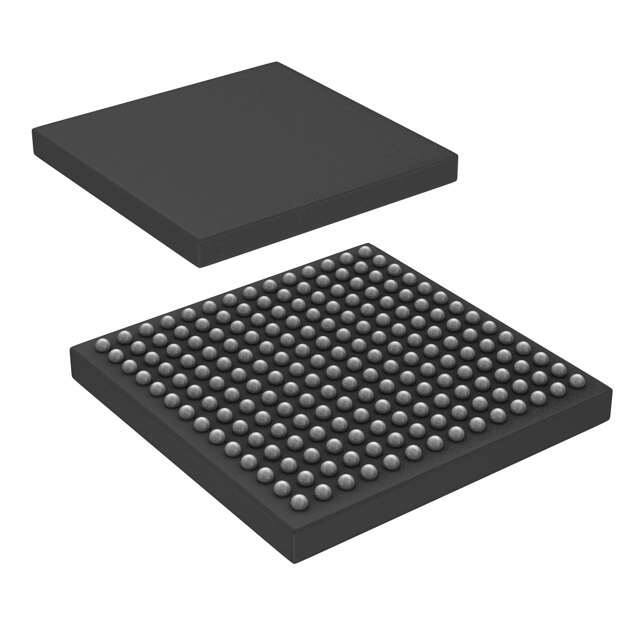


 工商网监
湘ICP备2023018690号
工商网监
湘ICP备2023018690号
