EUP3458
1.2A,30V,1.2MHz Step-Down Converter
DESCRIPTION
FEATURES
The EUP3458 is current mode, step-down switching
regulator capable of driving 1.2A continuous load with
excellent line and load regulation. The EUP3458 can
operate with an input voltage range from 4.5V to 30V
and the output can be externally set from 0.8V to 15V
with a resistor divider.
Fault protection includes cycle-by-cycle current
limiting and thermal shutdown. In shutdown mode the
regulator draws 1µA of supply current. Internal
soft-start minimizes the inrush current and the output
overshoot.
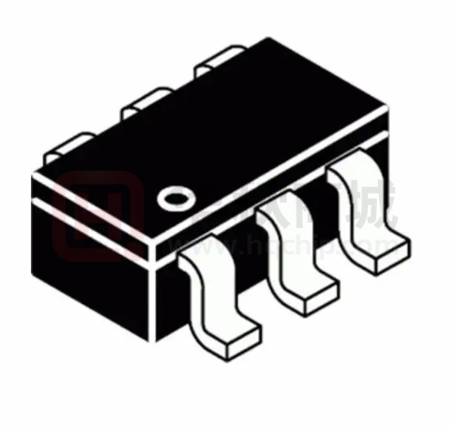
The EUP3458 is available in SOT23-6 and TSOT23-6
packages.
�
�
�
�
�
�
�
�
�
�
�
1.2A Output Current
0.3Ω Internal DMOS Output Switch
4.5V to 30V Input Operating Range
Output Adjustable from 0.8V to 15V
Up to 92% Efficiency
1µA Shutdown Current
Fixed 1.2MHz Frequency
Thermal Shutdown and Overcurrent Protection
Input Supply Undervoltage Lockout
Available in SOT23-6 and TSOT23-6 Packages
RoHS Compliant and 100% Lead(Pb)-Free
Halogen-Free
APPLICATIONS
�
�
�
�
Distributed Power Systems
Battery Charger
Pre-Regulator for Linear Regulators
WLED Drivers
Typical Application Circuit
Figure 1. 12V/24V to 3.3V Application Circuit
DS3458
Ver0.2
Apr. 2011
1
�EUP3458
Typical Application Circuit (continued)
Figure 2. 12V/24V to 5V Application Circuit
Pin Configurations
Package Type
Pin
Configurations
SOT23-6
TSOT23-6
Pin Description
Pin
Name
SOT23-6
TSOT23-6
BS
1
1
GND
2
2
FB
3
3
EN
4
4
IN
5
5
SW
6
6
DS3458
Ver0.2
Apr. 2011
DESCRIPTION
High-Side Gate Driver Boostrap Supply. BS provides power to the gate
driver of n-channel MOSFET switch. Connect a 10nF or greater
capacitor from SW to BS.
Ground. This pin is the voltage reference for the regulated output
voltage. It should be kept away from the D1 and input capacitor for noise
prevention.
Output Feedback Input. FB senses the output voltage to regulate that
voltage. Connect FB to an external resistor divider to set the output
voltage. The value of the divider resistors also set loop bandwidth.
Enable Input. EN is a logic input that controls the regulator on or off.
Drive EN logic high to turn on the regulator, and set EN logic low to
turn it off. Don't leave EN pin floating. Directly connect EN to IN (or
through a resistance) for automatic startup.
Input Supply Pin. IN supplies the power to the IC and the power
switch. Connect IN to a 4.5V to 30V power source. Bypass IN to
GND with a suitably large value capacitor to minimize input ripple
to the IC.
Power Switcher Output. Connect the output LC filter from SW to the
output.
2
�EUP3458
Ordering Information
Order Number
Package Type
EUP3458VIR1
SOT23-6
EUP3458OIR1
TSOT23-6
Marking
xxxxx
AZ00
xxxxx
AZ00
EUP3458 □ □ □ □
Lead Free Code
1: Lead Free, Halogen Free
0: Lead
Packing
R: Tape & Reel
Operating temperature range
I: Industry Standard
Package Type
V: SOT
O: TSOT
Block Diagram
Figure 3. Functional Block Diagram
DS3458
Ver0.2
Apr. 2011
3
Operating Temperature Range
-40°C to +85°C
-40°C to +85°C
�EUP3458
Absolute Maximum Ratings (1)
Input Voltage (VIN) ----------------------------------------------------------------- -0.3V to 35V
Enable Input (VEN) ----------------------------------------------------------------- -0.3V to 35V
Switch Voltage (VSW) ------------------------------------------------------ -1V to VIN +0.3V
Boot Strap Voltage (VBS) ------------------------------------------------ VSW-0.3V to VSW +6V
All Other Pins --------------------------------------------------------------------- -0.3V to 6V
Junction Temperature ------------------------------------------------------------------- 150°C
Storage Temperature ------------------------------------------------------ -65°C to +150°C
Lead Temp (Soldering, 10sec) ------------------------------------------------------260°C
Thermal Resistance θJA (SOT23-6) ------------------------------------------------- 205°C/W
Thermal Resistance θJA (TSOT23-6) ----------------------------------------------- 200°C/W
�
�
�
�
�
�
�
�
�
�
Recommend Operating Conditions (2)
Supply Voltage (VIN) ------------------------------------------------------------- 4.5V to 30V
Operating Temperature Range ----------------------------------------------- -40°C to +85°C
�
�
Note (1): Stress beyond those listed under “Absolute Maximum Ratings” may damage the device.
Note (2): The device is not guaranteed to function outside the recommended operating conditions.
Electrical Characteristics
The ● denote specifications which apply over the full operating temperature range, otherwise specifications are
TA=+25°C. VEN=5V, VIN=12V unless otherwise specified.
Parameter
Conditions
Feedback Voltage
4.5V ≤ VIN ≤ 30V
Shutdown Supply Current
VEN=0V
Operating Supply Current
VEN=2V,VFB=1V, VBS=10V
Min.
●
0.800
0.816
0.776
0.800
0.824
1
5
µA
0.55
1
mA
VEN=0V, VSW=0V
Oscillator Frequency
5
1.6
2.1
1
1.2
V
Ω
0.3
Switch Peak Current Limit
Unit
0.784
Switch On Resistance
Switch Leakage
EUP3458
Typ.
Max.
µA
A
1.4
MHz
Short Circuit Frequency
VFB=0V
450
KHz
Maximum Duty Cycle
VFB=0.7V
90
%
100
ns
Minimum On-Time
Enable Low Voltage
0.4
Enable High Voltage
Input Undervoltage Lockout Threshold
Input Undervoltage Lockout Threshold
Hysteresis
Enable Leakage Current
1.5
In Rising
3.3
Ver0.2
Apr. 2011
3.9
300
VEN=0V
0.1
Thermal Shutdown
DS3458
3.6
165
4
V
V
mV
5
µA
°C
�EUP3458
Typical Operating Characteristics
VIN=12V, VOUT=3.3V, C1 =10µF, C2=22µF, L1=4.7µH, TA=25°C, unless otherwise noted.
Figure4.
Figure5.
Figure6.
Figure7.
Figure8.
DS3458
Ver0.2
Apr. 2011
Figure9.
5
�EUP3458
Typical Operating Characteristics (continued)
VIN=12V, VOUT=3.3V, C1 =10µF, C2=22µF, L1=4.7µH, TA=25°C, unless otherwise noted.
Figure11.
Figure10.
DS3458
Ver0.2
Apr. 2011
Figure12.
Figure13.
Figure14.
Figure15.
6
�EUP3458
Typical Operating Characteristics (continued)
VIN=12V, VOUT=3.3V, C1 =10µF, C2=22µF, L1=4.7µH, TA=25°C, unless otherwise noted.
Figure16.
DS3458
Ver0.2
Apr. 2011
Figure17.
7
�EUP3458
Functional Description
The EUP3458 is current-mode step-down switching
regulator. The device regulates an output voltage as low
as 0.8V from a 4.5V to 30V input power supply. The
device can provide up to 1.2Amp continuous current to
the output. The EUP3458 uses current-mode architecture
to control the regulator loop. The output voltage is
measured at FB through a resistive voltage divider and
amplified through the internal error amplifier.
Slope compensation is internally added to eliminate
subharmonic oscillation at high duty cycle. The slope
compensation adds voltage ramp to the inductor current
signal which reduces maximum inductor peak current at
high duty cycles.
The device uses an internal n-channel switch to step
down the input voltage to the regulated output voltage.
Since the n-channel switch requires gate voltage greater
than the input voltage, a boostrap BS capacitor is
connected between SW and BS to drive the n-channel
gate.
Application Information
Setting the Output Voltage
The output voltage is set through a resistive voltage
divider (see Figure1 or 2). The voltage divider divides
the output voltage down by the ratio:
VFB = VOUT ∗ R 2 / (R1 + R 2 ) = 0.8V
VOUT = 0.8V ∗ (R1 + R 2 ) / R 2
The feedback resistor R1 also sets the feedback loop
bandwidth with the internal compensation capacitor. R2
can be determined by:
R 2 = R1(VOUT / 0.8 − 1)
Inductor
The inductor is required to supply constant current to the
output load while being driven by the switched input
voltage. A larger value inductor results in less ripple
current and lower output ripple voltage. However, the
larger value inductor has a larger physical size, higher
series resistance, and lower saturation current. Choose
an inductor that does not saturate under the worst-case
load conditions. A good rule for determining the
inductance is to allow the peak-to- peak ripple current in
the inductor to be approximately 30% of the maximum
load current. Also, make sure that the peak inductor
current (the load current plus half the peak-to-peak
inductor ripple current) is below the 2A minimum peak
current limit.
The inductance value can be calculated by the equation:
L = (VOUT ) ∗ (VIN − VOUT ) / (VIN ∗ f ∗ ∆I )
Ver0.2
Apr. 2011
Input Capacitor
The input current to the step-down converter is
discontinuous, and therefore an input capacitor C1 is
required to supply the AC current to the step-down
converter while maintaining the DC input voltage. A low
ESR capacitor is required to keep the noise minimum at
the IC. Ceramic capacitors are preferred, but tantalum or
low-ESR electrolytic capacitors may also suffice. The
input capacitor value should be greater than 10µF, and
the RMS current rating should be greater than
approximately 1/2 of the DC load current. In Figure 1 or
2, all ceramic capacitors should be placed close to the
EUP3458.
Output Capacitor
The output capacitor is required to maintain the DC
output voltage. Low ESR capacitors are preferred to
keep the output voltage ripple low. The characteristics of
the output capacitor also affect the stability of the
regulator control loop. In the case of ceramic capacitors,
the impedance at the switching frequency is dominated
by the capacitance. For most application, a 22µF
ceramic capacitor will be sufficient.
Output Rectifier Diode
Thus the output voltage is :
DS3458
Where VOUT is the output voltage, VIN is the input
voltage, f is the switching frequency, and ∆I is the
peak-to-peak inductor ripple current.
8
The output rectifier diode supplies the current to the
inductor when the switch is off. A schottky diode is
recommended to reduce losses due to the diode forward
voltage and recovery times. The reverse voltage rating of
the diode should be greater than the maximum input
voltage, and current rating should be greater than the
maximum load current.
External Boostrap Diode
An external boostrap diode may improve the efficiency
when input voltage is lower than 5.5V or duty cycle is
higher than 65%. The external 5V can be a 5V fixed
input from system or a 5V output of the EUP3458.
�EUP3458
Thermal Considerations
To avoid the EUP3458 from exceeding the maximum
junction temperature, the user will need to do a thermal
analysis. The goal of the thermal analysis is to determine
whether the operating conditions exceed the maximum
power dissipation which can be calculated by following
formula:
PL ( MAX ) = (TJ ( MAX ) − TA ) / θ JA
Where TJ(MAX) is the maximum operation junction
temperature, TA is the ambient temperature and the θJA is
the junction to ambient thermal resistance.
Table 1. External components for typical designs
Vin(V)
Vout(V)
L1(µ H)
C2(µ F)
5
1.2
2.2
22
180
360
5
1.8
3.3
22
62
49.9
12
1.8
3.3
22
62
49.9
12
3.3
4.7
22
75
24
12
5
6.8
22
68
13
24
3.3
4.7
22
75
24
R1(KΩ) R2(KΩ)
24
5
6.8
22
68
13
To simplify design efforts using the EUP3458, the typical
designs for common applications are listed in Table 1.
DS3458
Ver0.2
Apr. 2011
9
�EUP3458
Packaging Information
SOT23-6
A
MILLIMETERS
MIN.
MAX.
1.45
MIN.
-
MAX.
0.057
A1
0.00
0.15
0.000
0.006
b
0.30
0.50
0.012
0.020
SYMBOLS
DS3458
Ver0.2
Apr. 2011
INCHES
D
2.90
0.114
E1
1.60
0.063
e
0.95
0.037
E
2.60
3.00
0.102
0.118
L
0.3
0.60
0.012
0.024
10
�EUP3458
TSOT23-6
A
A1
b
MILLIMETERS
MIN.
MAX.
1.00
0.00
0.15
0.30
0.50
D
2.90
0.114
E1
e
E
1.60
0.95
0.063
0.037
2.60
3.00
0.102
0.118
L
0.3
0.60
0.012
0.024
SYMBOLS
DS3458
Ver0.2
Apr. 2011
11
INCHES
MIN.
0.000
0.012
MAX.
0.039
0.006
0.020
�


 工商网监
湘ICP备2023018690号
工商网监
湘ICP备2023018690号

