www.fairchildsemi.com
AN-6075
Compact Green-Mode Adapter Using FSQ500L for Low Cost
1. Introduction
This application note describes a detailed design strategy for a compact flyback converter. Design considerations and mathematical equations are presented, as well as guidelines for a printed circuit board layout. The FSQ500L is designed for a replacement of linear power supplies to achieve low cost. This device combines current-mode Pulse Width Modulator (PWM) with a single-chip 700V senseFET. The integrated PWM controller features include: fixed operating frequency (130KHz), under-voltage lockout (UVLO) protection, soft-start time tuned by external capacitor, overload protection (OLP), leading-edge blanking (LEB), optimized gate turn-on/turn-off driver, thermal shutdown (TSD) protection with hysteresis, and temperaturecompensated precision-current sources for loop compensation. The no-load power consumption can be less than 250mW without auxiliary bias winding and down to 60mW with auxiliary bias winding for universal AC input voltage range to meet the power conservation requirements. When compared to a linear power supply, the FSQ500L reduces total size and weight, while increasing efficiency, productivity, and system reliability. This device provides a platform for cost-effective flyback converters.
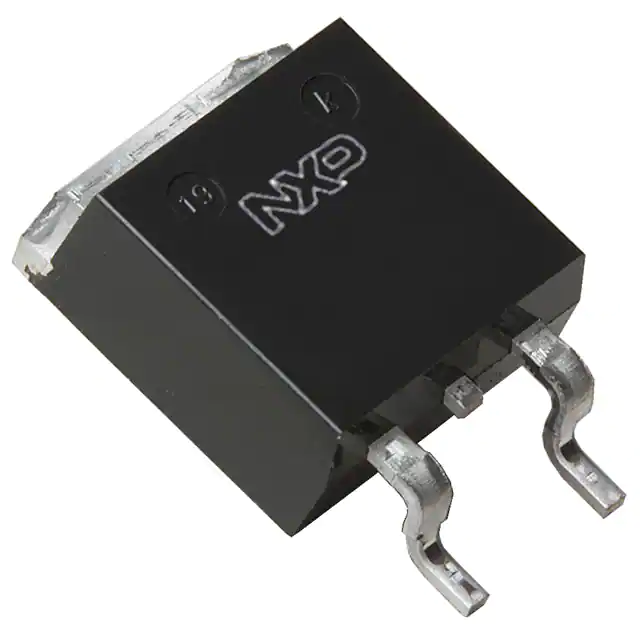
Figure 1.
SOT-223 Pin Configuration
Figure 2.
Typical Application
© 2008 Fairchild Semiconductor Corporation Rev. 1.0.0 • 9/11/08
www.fairchildsemi.com
�AN-6075
APPLICATION NOTE
2. Device Block Description
2.1 Startup Circuit and Soft Start
At startup, an internal high-voltage current source supplies the internal bias and charges the external capacitor (Ca) connected to the VCC pin, as illustrated in Figure 4. An internal high-voltage regulator (HV/REG) located between the D and VCC pins regulates the VCC to be 6.5V and supplies operating current. FSQ500L needs no auxiliary bias winding.
Transformer D
progressively increased with the intention of smoothly establishing the required output voltage. It also helps to prevent transformer saturation and reduce the stress on the secondary diode during startup.
2.2 Feedback Control
FSQ500L employs current-mode control, as shown in Figure 5. An opto-coupler (such as the FOD817A) and shunt regulator (such as the KA431) are typically used to implement the feedback network. Comparing the feedback voltage with the voltage across the Rsense resistor makes it possible to control the switching duty cycle. When the reference pin voltage of the shunt regulator exceeds the internal reference voltage of 2.5V, the opto-coupler LED current increases, pulling down the feedback voltage and reducing the duty cycle. This typically occurs when the line input voltage increases or the output load current decreases.
2
VCC Ca
3
6.5V
ICH HV/REG ISTAR T
VREF
UVLO
2.3 Pulse-by-Pulse Current Limit
Because current-mode control is employed, the peak current through the senseFET is limited by the non-inverting input of PWM comparator (Vfb*), as shown in Figure 5. Assuming that 225µA current source flows only through the internal resistor (8R + R = 12 kΩ), the cathode voltage of diode D2 is about 2.7V. Since D1 is blocked when the feedback voltage (Vfb) exceeds 2.7V, the maximum voltage of the cathode of D2 is clamped at this voltage, clamping Vfb*. Therefore, the peak value of the current through the senseFET is limited.
VCC VCC IFB
OS C
Figure 3.
Startup Block
The soft-start time of FSQ500L is tuned by an external VCC capacitor (Ca), which increases PWM comparator noninverting input voltage, together with the senseFET current, slowly after it starts up. Before VCC reaches VSTART, Ca is charged by the current ICH-ISTART, where ICH and ISTART are described in Figure 3. After VCC reaches VSTART, all internal blocks are activated, so that the current consumed inside the IC becomes IOP. Therefore, Ca is charged by the current ICHIOP, which makes the increasing slope of VCC become sluggish. Make the soft-start time long or short by selecting Ca as described in Figure 4. During tS/S, IDELAY is disabled to avoid unwanted OLP. Typically, tS/S is around 8ms with 47µF of Ca.
VCC 6.5V 6V 5V tS/S
IDELAY
vo
FOD817A R1
Vfb
CB
2
S enseFE T
D1
D2 + Vfb*
8R R Gate driver
CF KA431 R2
-
VC C R E G VS T AR T VS T O P
VSD
O LP
Rsense
Figure 5.
Pulse-Width Modulation (PWM) Circuit
2.4 Leading-Edge Blanking (LEB)
t1 t1=Ca×6V/(IC H - IS T AR T ) t2 tS/S=Ca×0.5V/(IC H -IO P ) t
Figure 4.
Soft-Start Function
The peak value of the drain current of the power switching device is progressively increased to establish the correct working conditions for transformers, inductors, and capacitors. The voltage on the output capacitors is
© 2008 Fairchild Semiconductor Corporation Rev. 1.0.0 • 9/11/08 2
At the instant the internal senseFET is turned on, a highcurrent spike occurs through the senseFET, caused by primary-side capacitance and secondary-side rectifier reverse recovery. Excessive voltage across the Rsense resistor would lead to incorrect feedback operation in the current mode PWM control. To counter this effect, the FSQ500L employs a leading-edge blanking (LEB) circuit. This circuit inhibits the PWM comparator for a short time (tLEB=250ns) after the senseFET turns on.
www.fairchildsemi.com
�AN-6075
APPLICATION NOTE
2.5 Protection Functions
The FSQ500L has two self-protective functions: overload protection (OLP) and thermal shutdown (TSD). While OLP is implemented as auto-restart mode, there is no switching when TSD triggers. Once the overload condition is detected, switching is terminated, the senseFET remains off, and HV/REG turns off. This causes VCC to fall. When VCC falls down to the under-voltage lockout (UVLO) stop voltage of 5.0V, the protection is reset and the startup circuit charges VCC capacitor. When VCC reaches the start voltage of 6.0V, the FSQ500L resumes normal operation. If the fault condition is still not removed, the senseFET and HV/REG remain off and VCC drops to VSTOP again. In this manner, the auto-restart can alternately enable and disable the switching of the power senseFET until the fault condition, is eliminated, as shown in Figure 6. Because these protection circuits are fully integrated into the IC without external components, the reliability can be improved without increasing cost.
Vds
Power on OLP occurs OLP removed
VCC. In this condition, Vfb continues increasing until it reaches 4.5V, when the switching operation is terminated, as shown in Figure 7.
Vfb
4.5V
Overload protection
2.7V
T1 2= CB *(4.5-2.7)/ID E L A Y
T1
T2
t
Figure 7.
Overload Protection
The OLP delay time is:
t 12 = C B • (4.5 - 2.7 ) IDelay (1)
Under 50ms delay time (the CB value should be smaller than 138nF) is applied for most applications. This protection is implemented in auto restart mode.
Vcc
6.5V 6.0V 5.0V
2.5.2 Thermal Shutdown (TSD)
The senseFET and the control IC are built in one package. This makes it easy for the control IC to detect the abnormal over-temperature of the senseFET. When the temperature exceeds approximately 140°C, thermal shutdown triggers.
Vds
Power on TSD occurs TSD removed
t
Normal operation Fault situation Normal operation
Figure 6.
Auto-Restart Protection Waveforms
2.5.1 Overload Protection (OLP)
Overload is defined as the load current exceeding normal level due to an unexpected abnormal event. In this situation, the protection circuit should trigger to protect the SMPS. However, even when the SMPS is in normal operation, the over load protection circuit can be triggered during the load transition. To avoid this undesired operation, the overload protection circuit is designed to trigger after a specified time to determine whether it is a transient situation or an overload situation. Because of the pulse-by-pulse current limit capability, the maximum peak current through the senseFET is limited and, therefore, the maximum input power is restricted with a given input voltage. If the output consumes more than this maximum power, the output voltage (VO) decreases below the set voltage. This reduces the current through the opto-coupler LED, which also reduces the opto-coupler transistor current, increasing the feedback voltage (Vfb). If Vfb exceeds 2.7V, D1 is blocked and the 5µA current source starts to charge CB slowly up to
© 2008 Fairchild Semiconductor Corporation Rev. 1.0.0 • 9/11/08 3
Vcc
6.5V 6.0V 5.7V
t
Normal operation Fault situation Normal operation
Figure 8.
Over-Temperature Protection
When TSD triggers, delay current is disabled, switching operation stops, and VCC through the internal high-voltage current source is set to 5.7V from 6.5V, as shown in Figure 8. Since the TSD signal prohibits the senseFET from switching, there is no switching until the junction temperature decreases sufficiently. If the junction temperature is lower than 60°C typically, the TSD signal is removed and VCC is set to 6.5V again. While VCC increases
www.fairchildsemi.com
�AN-6075
APPLICATION NOTE
from 5.7V to 6.5V, the soft-start function turns the senseFET on and off with no voltage and/or current stress.
3.2 Determine DC Link Capacitor (CDC) and DC Link Voltage Range
It is typical to select the DC link capacitor as 2-3µF per watt of input power for universal input range (85-264VAC) and 1µF per watt of input power for European input range (195264VAC). Figure 10 shows the corrected input voltage waveform. The red line shows ripple voltage on the DC link capacitor and the minimum and maximum voltage on the DC link capacitor are expressed in Equations 2 and 3.
2.6 Burst Operation
To minimize power dissipation in standby mode, the FSQ500L enters burst-mode operation. As the load decreases, the feedback voltage decreases. As shown in Figure 10, the device automatically enters burst mode when the feedback voltage drops below VBURL (750mV). At this point, switching stops and the output voltages start to drop at a rate dependent on standby current load. This causes the feedback voltage to rise. Once it passes VBURH (800mV), switching resumes. The feedback voltage then falls and the process repeats. Burst-mode operation alternately enables and disables switching of the power senseFET, thereby reducing switching loss in standby mode.
Vo
V os et
Figure 10.
Vfb
0.80V 0.75V
Bridge Rectifier and Bulk Capacitor Voltage Waveform
VDC,min = 2Vac,min 2 -
2VO × IO × (1 - D ch ) η × C DC × 2fL 2 × 5.1V × 0.4A × (1 - 0.3) 0.5 × 5.7 μF × 120Hz (2)
= 2 × 85Vac 2 I ds
= 87V
VDC,max = 2Vac,max = 2 × 264V = 373V
V ds
(3)
where Dch is DC link capacitor charging duty ratio defined as shown in Figure 10, which is typically about 0.3. Output power is 2.04W, so the VDC capacitor is 6.08µF. Select the nearest standard value 5.7µF (4.7µF+1µF) for CDC and substitute it above. Therefore; from Equation 2 and 3, the VDC,min is 87V and VDC,max is 373V.
time
t1
S witching disabled
t2
t3
S witching disabled
t4
Figure 9.
Burst-Mode Operation
3.3 Determine the Turn Ratio
The transformer turn ratio (n=Npri/Nsec) is an important parameter of the flyback converter; it affects the maximum duty ratio when the input voltage is at a minimum value. It also influences the voltage stresses on the MOSFET and the secondary rectifier. The permissible voltage stresses and the maximum voltage stresses on the MOSFET, as well as the secondary rectifier, can be expressed as:
VDS,max = VDC,max + n(VO + VF ) = 373V + 11.5 × (5.1 + 0.7V ) V = 440V
3. Design Example
The following is design example for 2W compact adapter.
3.1 Determine System Specifications
Output Power, PO=2.04W (5.1V/0.4A); VAC input range=85 to 264VAC (universal input), line frequency, fL=60Hz; Efficiency, η>50%.
(4)
VDR,max =
VDC,max n
+ VO =
373V + 5.1 = 37.5V V 11.5
(5)
where VF is the forward-voltage of output diode.
© 2008 Fairchild Semiconductor Corporation Rev. 1.0.0 • 9/11/08 www.fairchildsemi.com 4
�AN-6075
APPLICATION NOTE
It is typical to set VDS,max as 420V~560V (60%~80% of MOSFET rated voltage). Select the transformer turn ratio, n, to be 11.5. According to Equation 4, VDS,max=440V, which satisfies 60%~80% of MOSFET rated voltage. The maximum voltage stress on the secondary rectifier can be calculated from Equation 5. Select SB260 rectifier diode from Equation 5 results. (Specification of SB260 as: the maximum reverse voltage, VRRM is 60V and average forward current, IF is 2A).
Base on Faraday’s law and the peak inductor current, the minimum turns for the primary inductance is calculated as:
NP,min =
=
L P × IPK × 10 6 B max × A e 800 μH × 0.28 A 0.24T × 19.2mm 2
× 10 6 = 48 Turns
(9)
where Bmax is the saturation magnetic flux density, typical set 0.2~0.3Tesla; Ae is the cross-sectional of the core.
3.4 Determine Transformer Primary-Side Inductance (LP), Maximum Duty (Dmax), and Primary RMS Current (IRMS)
The primary-side inductance (LP) of the transformer is designed specifically for DCM operation and obtained as:
LP = 2 × PO IPK × η × fS
2
3.6 Determine Secondary-Side Turns (NP,min)
The number of turns for the secondary winding is defined as:
NS = NP 104 = ≅ 9 Turns n 11.5 (10)
=
V 2 × 5 .1 × 0 .4 A
(0.28 A)
2
× 0.5 × 130KHz
≅ 800 μH
(6)
Select primary-side turns, NP to be 104 turns, so the secondary-side turns is 9 turns, based on Equation 10.
where IPK is primary-side peak current, given in the datasheet as ILIM. The maximum duty ratio (Dmax) can be derived as:
Dmax = LP × fS × IPK 800μ0 × 130kHz × 0.28A = = 33% VDC,min 87V
3.7 Determine Primary-Side RCD Snubber
When the MOSFET turns off, a high-voltage spike occurs on the drain pin because of a resonance between the leakage inductor (Llk) of the main transformer and the output capacitor (Coss) of the MOSFET. The excessive voltage on the drain pin may lead to an avalanche breakdown and eventually damage the MOSFET. Therefore, it is necessary to add an additional circuit to clamp the voltage. The RCD snubber circuit and MOSFET drain voltage waveforms are shown in Figure 11 and Figure 12, respectively. The RCD snubber circuit absorbs the current in the leakage inductor by turning on the snubber diode (Dsn) when VDS exceeds Vin+nVO. It is assumed that the snubber capacitance is large enough that its voltage does not change during one switching period. The Rsn2 can reduce the spike damping wave and affect EMI.
(7)
The maximum duty ratio should be kept below 50% for DCM operation. The primary-side RMS current can be derived as:
IRMS = IPK × D max 0.33 = 0.28 × = 0.09 A 3 3 (8)
3.5 Determine Transformer Core Size (Ae) and Minimum Primary-Side Turns (NP,min)
Table 1 shows the commonly used cores with output power under 10W. The cores recommended are typical for the universal input range and 130kHz switch frequency. Choose the EE16 core to meet this output power from Table 1.
Table 1. Core Quick Select Table (for universal input, fS=130KHz and 5V output)
Core
EE13-Z EI16-Z EE16-Z EI19-Z
CrossSectional Area (Ae)
17.1mm 19.8mm 19.2mm 24.0mm
2 2 2 2
Window Area (Aw)
33.4mm 42.3mm
2
Output Power Range
1-5W 1-5W 1-10W 1-10W
Figure 11. Primary-Side RCD Snubbber Circuit
2
39.8mm 54.4mm
2 2
© 2008 Fairchild Semiconductor Corporation Rev. 1.0.0 • 9/11/08
www.fairchildsemi.com 5
�AN-6075
APPLICATION NOTE
3.8 External VCC Auxiliary Winding Circuit for Improving Power Saving
Figure 13 shows an external VCC auxiliary winding circuit for improving power saving. The external VCC auxiliary winding circuit reduces internal circuit power loss to improve power saving.
Figure 12.
MOSFET Drain Voltage Waveform
The snubber capacitor voltage (Vsn) should be determined at the minimum input voltage and full-load condition. Once Vsn is determined, the power dissipated in the snubber circuit at the minimum input voltage and full-load condition is obtained by:
Loss sn V2 1 Vsn = sn = Llk × I pk 2 × fS × Rsn 2 Vsn − nVO
Figure 13.
(11)
External VCC Auxiliary Winding Circuit for Improving Power Saving
where fS is the switching frequency of FSQ500L. Vsn should be 2~2.5 times of nVO. Very small Vsn results in a severe loss in the snubber circuit, as shown Equation 11. The resistance is obtained by:
Rsn = Vsn 1 Llk × I pk 2 × fS × 2 Vsn − nVO 130 2 (12) Vsn 2
The number of turns for the VCC auxiliary winding is defined as:
Naux = VA + VD 2F 7.7 + 0.7 × NS = × 9 ≅ 13 Turns 5.1 + 0.7 VO + VF
(15)
where VA is the voltage of VCC auxiliary winding and VD2F is forward-voltage of D2 diode. Because the FSQ500L has an internal high-voltage regulator (HV/REG) located between the D and VCC pins that regulates the VCC to be 6.5V and supplies operating current. If using the auxiliary winding, the VCC should be set higher than 6.5V. Assume VA is 7.7V and VCC is 6.8V, according to Equation 15, Naux = 13 turns is solved. The RCF is limited operation current; it can be obtained as:
RF ≤ VA - VCC 7.7 - 6.8 = = 1.18K Ω , using 1KΩ IOP 760 μA
=
130 0.5 × 90 μH × 0.28A 2 × 130kHz × 130 - 11.55 × 5.1 = 20kΩ
The power loss from Rsn can be calculated as:
Psn V2 130 = sn = ≅ 0.845W Rsn 20kΩ (13)
(16)
where IOP is operation current, in the datasheet as IOP. In this circuit, a smaller capacitor C1 (~1µF) can be used to reduce startup time. The energy supporting the FSQ500L after startup is mainly from a larger capacitor C2 (~22µF). In this design example, if using the VCC auxiliary winding, the no-load power saving is down to 60mW.
Note: 1. If using the external VCC auxiliary circuit, the VSD voltage of FB pin follows as VCC voltage.
To reduce the power loss from Rsn, the Rsn should be selected higher than 20kΩ. From Equation 12 if the Rsn increases, the Vsn also increases, the Rsn recommended value is between 200kΩ and 47kΩ. The maximum ripple of the snubber capacitor voltage is obtained as:
C sn =
=
Vsn ΔVsn × Rsn × fs
130 ≅ 0.7nF , selected 1nF 5% × 130 × 200kΩ × 130kHz
(14)
where fs is the switching frequency and Rsn uses 200kΩ. In general, 5~10% ripple is reasonable.
© 2008 Fairchild Semiconductor Corporation Rev. 1.0.0 • 9/11/08 www.fairchildsemi.com 6
�AN-6075
APPLICATION NOTE
4. Printed Circuit Board Layout
High-frequency switching current / voltage makes printed circuit board layout a very important design issue. Good PCB layout minimizes excessive EMI helps the power supply survive during surge/ESD tests. Two suggestions with different pro and cons for ground connections are recommended. GND2→1: This could avoid common impedance interference for the sense signal. Regarding the ESD discharge path, the charges go from secondary, through the transformer stray capacitance, to GND1 first, and back to mains. It should be noted that control circuits should not be placed on the discharge path. Point discharge for common choke can decrease high-frequency impedance and increase ESD immunity. 3 should be a point-discharger route to bypass the static electricity energy. As shown in Figure 12, it is suggested to map out this discharge route. Should a Y-cap be required between primary and secondary, connect this Y-cap to the positive terminal of CDC. If this Y-cap is connected to primary GND, it should be connected to the negative terminal of CDC (GND1) directly. Point discharge of this Y-cap helps for ESD; however, the creepage between these two pointed ends should be at least 5mm according to safety requirements.
4.1 Guidelines
To improve EMI performance and reduce line frequency ripples, the output of the bridge rectifier should be connected to capacitor CDC first, then to the switching circuits. Refer to Figure 14. The high-frequency current loop is in CDC – Transformer – Drain PIN – GND PIN – CDC. The area enclosed by this current loop should be as small as possible. Keep the traces (especially 2→1) short, direct, and wide. Highvoltage traces related the drain of MOSFET and RCD snubber should be kept far way from control circuits to prevent unnecessary interference. If a heatsink is used for MOSFET, connect this heatsink to ground. As indicated by 2, the ground of control circuits should be connected first, then to other circuitry. Place Ca close to the controller for good decoupling.
Figure 14.
Layout Considerations
© 2008 Fairchild Semiconductor Corporation Rev. 1.0.0 • 9/11/08
www.fairchildsemi.com 7
�AN-6075
APPLICATION NOTE
5. Typical Application Circuit
Application
Adapter
Output Power
2.04W
Input Voltage Range
Universal Input (85-264VAC)
Output Voltage/Maximum Current
5.1V/0.4A
5.1 Features
Single Chip 700V SenseFET Power Switch Soft-Start Time Tuned by External Capacitor Built-in Overload Protection (OLP) and Internal Thermal Shutdown Function (TSD) with Hysteresis Low Standby Mode Power Consumption (Input Wattage


 工商网监
湘ICP备2023018690号
工商网监
湘ICP备2023018690号