www.fairchildsemi.com
KM4110/KM4120
0.5mA, Low Cost, +2.7V & +5V, 75MHz Rail-to-Rail Amplifiers
Features
■
■
■
■
■
■
■
■
■
■
■
■
General Description
505µA supply current
75MHz bandwidth
Power down to Is = 33µA (KM4120)
Fully specified at +2.7V and +5V supplies
Output voltage range: 0.07V to 4.86V; Vs = +5
Input voltage range: -0.3V to +3.8V; Vs = +5
50V/µs slew rate
±15mA linear output current
±30mA output short circuit current
12nV/√Hz input voltage noise
Directly replaces AD8031 in single
supply applications
Small package options (SOT23-5 and SOT23-6)
Applications
■
■
■
■
■
Portable/battery-powered applications
A/D buffer
Active filters
Signal conditioning
Portable test instruments
The KM4110 (single) and KM4120 (single with disable)
are low cost, voltage feedback amplifiers. These
amplifiers are designed to operate on +2.7V, +5V, or
±2.5V supplies. The input voltage range extends
300mV below the negative rail and 1.2V below the
positive rail.
The KM4110 offers superior dynamic performance
with a 75MHz small signal bandwidth and 50V/µs
slew rate. The combination of low power, high
output current drive, and rail-to-rail performance
make the KM4110 well suited for battery-powered
communication/ computing systems.
The combination of low cost and high performance
make the KM4110 suitable for high volume applications in both consumer and industrial applications
such as wireless phones, scanners, and color copiers.
The KM4210 dual op amp is also available.
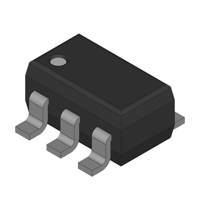
SOT23-5 (KM4110)
1
-Vs
2
+In
3
+
Out
5
+Vs
4
-In
-
Normalized Magnitude (1dB/div)
Non-Inverting Freq. Response Vs = +5V
KM4110/KM4120 Packages
G=2
Rf = 1kΩ
0.1
SOT23-6 (KM4120)
1
10
100
Frequency (MHz)
1
-Vs
2
+In
3
+
Out
-
6
+Vs
5
DIS
4
-In
REV. 1C October 2001
�DATA SHEET
KM4110/KM4120
KM4110/KM4120 Electrical Characteristics
Parameters
(Vs = +2.7V, G = 2, RL = 1kΩ to Vs/2, Rf = 1kΩ; unless noted)
Conditions
Case Temperature
Frequency Domain Response
-3dB bandwidth
TYP
Min & Max
+25°C
+25°C
UNITS
NOTES
1
G = +1, Vo = 0.05Vpp
G = +2, Vo < 0.2Vpp
G = +2, Vo = 2Vpp
65
30
12
28
MHz
MHz
MHz
MHz
Time Domain Response
rise and fall time
settling time to 0.1%
overshoot
slew rate
0.2V step
1V step
1V step,
2V step, G = -1
7.5
60
10
40
ns
ns
%
V/µs
Distortion and Noise Response
2nd harmonic distortion
3rd harmonic distortion
THD
input voltage noise
1Vpp, 1MHz
1Vpp, 1MHz
1Vpp, 1MHz
>10kHz
67
72
65
12
dBc
dBc
dB
nV/√Hz
full power bandwidth
gain bandwidth product
DC Performance
input offset voltage
average drift
input bias current
average drift
input offset current
power supply rejection ratio
open loop gain
quiescent current
Disable Characteristics
turn on time
turn off time
off isolation
quiescent current
Input Characteristics
input resistance
input capacitance
input common mode voltage range
common mode rejection ratio
Output Characteristics
output voltage swing
linear output current
short circuit output current
power supply operating range
DC
5MHz, RL = 100Ω
DC, Vcm = 0V to Vs - 1.5
RL = 10kΩ to Vs/2
RL = 1kΩ to Vs/2
0
10
1.2
3.5
30
66
98
470
±5
mV
µV/°C
µA
nA/°C
nA
dB
dB
µA
±3.5
350
60
65
600
0.54
4.3
58
15
µs
µs
dB
µA
9
1.5
-0.3 to 1.5
98
MΩ
pF
V
dB
0.05 to 2.6
0.09 to 2.53
±15
±25
2.7
78
0.2 to 2.35
2.5 to 5.5
V
V
mA
mA
V
2
2
2
2
2
2
2
2
Min/max ratings are based on product characterization and simulation. Individual parameters are tested as noted. Outgoing quality levels
are determined from tested parameters.
NOTES:
1) For G = +1, Rf = 0.
2) 100% tested at +25°C.
Absolute Maximum Ratings
supply voltage
0 to +6V
maximum junction temperature
+175°C
storage temperature range
-65°C to +150°C
lead temperature (10 sec)
+260°C
operating temperature range (recommended) -40°C to +85°C
input voltage range
+Vs +0.5V; -Vs -0.5V
internal power dissipation
see power derating curves
2
Package Thermal Resistance
Package
θJA
5 lead SOT23
6 lead SOT23
256°C/W
230°C/W
REV. 1C October 2001
�KM4110/KM4120
DATA SHEET
KM4110/KM4120 Electrical Characteristics
PARAMETERS
CONDITIONS
Case Temperature
Frequency Domain Response
-3dB bandwidth
(Vs = +5V, G = 2, RL = 1kΩ to Vs/2, Rf = 1kΩ; unless noted)
TYP
+25°C
MIN & MAX UNITS
+25°C
G = +1, Vo = 0.05Vpp
G = +2, Vo < 0.2Vpp
G = +2, Vo = 2Vpp
75
35
15
33
MHz
MHz
MHz
MHz
Time Domain Response
rise and fall time
settling time to 0.1%
overshoot
slew rate
0.2V step
2V step
2V step,
2V step, G = -1
6
60
12
50
ns
ns
%
V/µs
Distortion and Noise Response
2nd harmonic distortion
3rd harmonic distortion
THD
input voltage noise
2Vpp, 1MHz
2Vpp, 1MHz
2Vpp, 1MHz
>10kHz
64
62
60
12
dBc
dBc
dB
nV/√Hz
full power bandwidth
gain bandwidth product
DC Performance
input offset voltage
average drift
input bias current
average drift
input offset current
power supply rejection ratio
open loop gain
quiescent current
Disable Characteristics
turn on time
turn off time
off isolation
quiescent current
Input Characteristics
input resistance
input capacitance
input common mode voltage range
common mode rejection ratio
Output Characteristics
output voltage swing
linear output current
short circuit output current
power supply operating range
DC
5MHz, RL = 100Ω
DC, Vcm = 0V to Vs - 1.5
RL = 10kΩ to Vs/2
RL = 1kΩ to Vs/2
-1
10
1.2
3.5
30
65
80
505
±5
±3.5
350
60
65
620
mV
µV/°C
µA
nA/°C
nA
dB
dB
µA
0.33
5.5
58
33
µs
µs
dB
µA
9
1.5
-0.3 to 3.8
92
MΩ
pF
V
dB
0.08 to 4.84
0.13 to 4.73
±15
±30
5
NOTES
78
0.2 to 4.65
2.5 to 5.5
V
V
mA
mA
V
1
2
2
2
2
2
2
2
2
Min/max ratings are based on product characterization and simulation. Individual parameters are tested as noted. Outgoing quality levels
are determined from tested parameters.
NOTES:
1) For G = +1, Rf = 0.
2) 100% tested at +25°C.
REV. 1C October 2001
3
�DATA SHEET
KM4110/KM4120
KM4110/KM4120 Performance Characteristics (Vs = +5V, G = 2, RL = 1kΩ to Vs/2, Rf = 1kΩ; unless noted)
G=1
Rf = 0
G=2
Rf = 1kΩ
G = 10
Rf = 1kΩ
G=5
Rf = 1kΩ
0.1
1
10
Inverting Freq. Response Vs = +5V
Normalized Magnitude (1dB/div)
Normalized Magnitude (1dB/div)
Non-Inverting Freq. Response Vs = +5V
G = -2
Rf = 1kΩ
G = -10
Rf = 1kΩ
G = -5
Rf = 1kΩ
G = -1
Rf = 1kΩ
0.1
100
1
Frequency (MHz)
G=1
Rf = 0
G=2
Rf = 1kΩ
G = 10
Rf = 2kΩ
G=5
Rf = 1kΩ
1
100
Inverting Freq. Response Vs = +2.7V
Normalized Magnitude (1dB/div)
Normalized Magnitude (2dB/div)
Non-Inverting Freq. Response Vs = +2.7V
0.1
10
Frequency (MHz)
10
G = -1
Rf = 1kΩ
G = -2
Rf = 1kΩ
G = -10
Rf = 1kΩ
G = -5
Rf = 1kΩ
0.1
100
1
10
100
Frequency (MHz)
Frequency (MHz)
Frequency Response vs. CL
Frequency Response vs. RL
RL = 1kΩ
CL = 20pF
Rs = 100Ω
CL = 100pF
Rs = 100Ω
CL = 50pF
Rs = 100Ω
+
Rs
-
CL
1kΩ
Magnitude (1dB/div)
Magnitude (1dB/div)
CL = 10pF
Rs = 0Ω
RL = 10kΩ
RL = 100Ω
RL
1kΩ
0.1
1
10
0.1
100
1
Frequency (MHz)
10
100
Frequency (MHz)
Large Signal Frequency Response
Frequency Response vs. Temperature
Magnitude (1dB/div)
Magnitude (1dB/div)
Vo = 1Vpp
Vo = 2Vpp
Vo = 4Vpp
0.1
1
10
Frequency (MHz)
4
100
0.01
0.1
1
10
100
Frequency (MHz)
REV. 1C October 2001
�KM4110/KM4120
DATA SHEET
KM4110/KM4120 Performance Characteristics (Vs = +5V, G = 2, RL = 1kΩ to Vs/2, Rf = 1kΩ; unless noted)
Input Voltage Noise
Open Loop Gain & Phase vs. Frequency
70
|Gain|
70
60
50
40
Phase
30
0
Open Loop Phase (deg)
Open Loop Gain (dB)
80
20
-45
10
-90
0
-135
-10
-180
100M
100
1k
10k
100k
1M
10M
Voltage Noise (nV/√Hz)
90
60
50
40
30
20
10
0
0.0001
0.001
1
10
-20
Vo = 1Vpp
Vo = 2Vpp
3rd
RL = 1kΩ
-30
3rd
RL = 150Ω
-40
-50
-60
2nd
RL = 1kΩ
2nd
RL = 150Ω
-70
3rd
RL = 1kΩ
-30
Distortion (dBc)
Distortion (dBc)
0.1
2nd & 3rd Harmonic Distortion; Vs = +2.7V
2nd & 3rd Harmonic Distortion; Vs = +5V
-20
3rd
RL = 150Ω
-40
-50
-60
2nd
RL = 1kΩ
-70
2nd
RL = 150Ω
-80
-80
-90
-90
0
1
2
3
4
0
5
1
2
2nd Harmonic Distortion vs. Vo
4
5
3rd Harmonic Distortion vs. Vo
-20
-30
-30
-40
-40
Distortion (dB)
-20
-50
-60
3
Frequency (MHz)
Frequency (MHz)
Distortion (dBc)
0.01
Frequency (MHz)
Frequency (Hz)
1MHz
-70
-50
-60
500kHz
-70
1MHz
500kHz
-80
100kHz
-80
100kHz
-90
-90
0.5
1
1.5
2
0.5
2.5
1.0
Output Amplitude (Vpp)
0
-10
-10
2.5
-20
CMRR (dB)
-20
PSRR (dB)
2.0
CMRR
PSRR
0
-30
-40
-50
-60
-30
-40
-50
-60
-70
-80
-70
-90
-80
-100
100
1k
10k
100k
1M
Frequency (Hz)
REV. 1C October 2001
1.5
Output Amplitude (Vpp)
10M
100M
100
1k
10k
100k
1M
10M
100M
Frequency (Hz)
5
�DATA SHEET
KM4110/KM4120
KM4110/KM4120 Performance Characteristics (Vs = +5V, G = 2, RL = 1kΩ to Vs/2, Rf = 1kΩ; unless noted)
Small Signal Pulse Response Vs = +5V
Output Current
Output Voltage (20mV/div)
Output Voltage (0.6V/div)
3
0
-3
50
0
Time (10ns/div)
-50
Output Current (10mA/div)
Large Signal Pulse Response Vs = +5V
Output Voltage (0.5V/div)
Output Voltage (20mV/div)
Small Signal Pulse Response Vs = +2.7V
Time (10ns/div)
Time (10ns/div)
Enable/Disable Response
Output Swing; Vs = +2.7V; G = -1
2.7
Output Voltage (0.5V/div)
Output Voltage (0.02V/div)
Vin = 0.2Vpp sinusoid
5V
Disable
Pulse
0V
Output
0
Time (1µs/div)
6
Time (1µs/div)
REV. 1C October 2001
�KM4110/KM4120
DATA SHEET
The design utilizes a patent pending topology that
provides increased slew rate performance. The common
mode input range extends to 300mV below ground
and to 1.2V below Vs. Exceeding these values will not
cause phase reversal. However, if the input voltage
exceeds the rails by more than 0.5V, the input ESD
devices will begin to conduct. The output will stay at
the rail during this overdrive condition.
The design uses a Darlington output stage. The output stage is short circuit protected and offers “soft”
saturation protection that improves recovery time.
The typical circuit schematic is shown in Figure 1.
6.8µF
+
-
Out
Rf
Rg
Figure 1: Typical Configuration
For optimum response at a gain of +2, a feedback resistor
of 1kΩ is recommended. Figure 2 illustrates the
KM4110 frequency response with both 1kΩ and 2kΩ
feedback resistors.
Enable/Disable Function (KM4120)
The KM4120 offers an active-low disable pin that can
be used to lower its supply current. Leave the pin
floating to enable the part. Pull the disable pin to the
negative supply (which is ground in a single supply
application) to disable the output. During the disable
condition, the nominal supply current will drop to
below 30µA and the output will be at high impedance
with about 2pF capacitance.
REV. 1C October 2001
1
10
100
Frequency (MHz)
Figure 2: Frequency Response vs. Rf
Power Dissipation
The maximum internal power dissipation allowed is
directly related to the maximum junction temperature.
If the maximum junction temperature exceeds 150°C,
some reliability degradation will occur. If the maximum
junction temperature exceeds 175°C for an extended
time, device failure may occur.
0.01µF
KM4110
Rf = 1kΩ
0.1
Maximum Power Dissipation (W)
+
Rf = 2kΩ
The KM4110 is short circuit protected. However, this
may not guarantee that the maximum junction temperature (+150°C) is not exceeded under all conditions. Follow the maximum power derating curves
shown in Figure 3 to ensure proper operation.
+Vs
In
G=2
RL = 1kΩ
Magnitude (1dB/div)
General Description
The KM4110 is a single supply, general purpose, voltage-feedback amplifier fabricated on a complementary
bipolar process. The KM4110 offers 75MHz unity gain
bandwidth, 50V/µs slew rate, and only 505µA supply
current. It features a rail-to-rail output stage and is
unity gain stable.
2.0
1.5
SOIC-8 lead
1.0
0.5
SOT23-5 lead
0
-50
-30
-10
10
30
50
70
90
Ambient Temperature ( C)
Figure 3: Power Derating Curves
Overdrive Recovery
For an amplifier, an overdrive condition occurs when
the output and/or input ranges are exceeded. The
recovery time varies based on whether the input or
output is overdriven and by how much the ranges are
exceeded. The KM4110 will typically recover in less
than 20ns from an overdrive condition. Figure 4
shows the KM4110 in an overdriven condition.
7
�DATA SHEET
KM4110/KM4120
Output
Input Voltage (0.5V/div)
Output Voltage (1V/div)
G=5
Input
Time (200ns/div)
Refer to the evaluation board layouts shown in Figure 7
for more information.
Evaluation Board Information
The following evaluation boards are available to aid
in the testing and layout of this device:
Eval Board
KEB002
Description
Products
Single Channel,
KM4110IT5,
Dual Supply 5 & 6 lead SOT23 KM4120IT6
Evaluation board schematics and layouts are shown in
Figure 6 and Figure 7.
Figure 4: Overdrive Recovery
Driving Capacitive Loads
The Frequency Response vs. CL plot on page 4,
illustrates the response of the KM4110 and KM4120. A
small series resistance (Rs) at the output of the amplifier,
illustrated in Figure 5, will improve stability and
settling performance. Rs values in the Frequency
Response vs. CL plot were chosen to achieve maximum
bandwidth with less than 1dB of peaking. For maximum
flatness, use a larger Rs.
+
The KEB002 evaluation board is built for dual supply
operation. Follow these steps to use the board in a
single supply application:
1. Short -Vs to ground
2. Use C3 and C4, if the -Vs pin of the KM4110 or
KM4120 is not directly connected to the
ground plane.
Rs
Rf
CL
RL
Rg
Figure 5: Typical Topology for driving
a capacitive load
Layout Considerations
General layout and supply bypassing play major roles
in high frequency performance. Fairchild has evaluation
boards to use as a guide for high frequency layout
and to aid in device testing and characterization.
Follow the steps below as a basis for high frequency
layout:
Include 6.8µF and 0.01µF ceramic capacitors
Place the 6.8µF capacitor within 0.75 inches
of the power pin
■ Place the 0.01µF capacitor within 0.1 inches
of the power pin
■ Remove the ground plane under and around the
part, especially near the input and output pins to
reduce parasitic capacitance
■ Minimize all trace lengths to reduce
series inductances
■
■
8
Figure 6: Evaluation Board Schematic
REV. 1C October 2001
�KM4110/KM4120
DATA SHEET
KM4110/KM4120 Evaluation Board Layout
Figure 7a: KEB002 (top side)
REV. 1C October 2001
Figure 7b: KEB002 (bottom side)
9
�DATA SHEET
KM4110/KM4120
b
CL
DATUM ’A’
KM4110/KM4120 Package Dimensions
e
2
SOT23-5
CL
CL
E
E1
α
e1
C
D
CL
1. All dimensions are in millimeters.
2 Foot length measured reference to flat
foot surface parallel to DATUM ’A’ and lead surface.
3. Package outline exclusive of mold flash & metal burr.
4. Package outline inclusive of solder plating.
5. Comply to EIAJ SC74A.
6. Package ST 0003 REV A supercedes SOT-D-2005 REV C.
A1
CL
MAX
1.45
0.15
1.30
0.50
0.20
3.10
3.00
1.75
0.55
0.95 ref
1.90 ref
0
10
NOTE:
A2
b
MIN
0.90
0.00
0.90
0.25
0.09
2.80
2.60
1.50
0.35
DATUM ’A’
A
SYMBOL
A
A1
A2
b
C
D
E
E1
L
e
e1
α
e
2
SOT23-6
CL
CL
E
α
e1
C
D
CL
A
10
A2
E1
SYMBOL
A
A1
A2
b
C
D
E
E1
L
e
e1
α
MIN
0.90
0.00
0.90
0.25
0.09
2.80
2.60
1.50
0.35
MAX
1.45
0.15
1.30
0.50
0.20
3.10
3.00
1.75
0.55
0.95 ref
1.90 ref
0
10
NOTE:
A1
1. All dimensions are in millimeters.
2 Foot length measured reference to flat
foot surface parallel to DATUM ’A’ and lead surface.
3. Package outline exclusive of mold flash & metal burr.
4. Package outline inclusive of solder plating.
5. Comply to EIAJ SC74A.
6. Package ST 0004 REV A supercedes SOT-D-2006 REV C.
REV. 1C October 2001
�KM4110/KM4120
DATA SHEET
Ordering Information
Model
Part Number
Package
Container
Partial Rail
KM4110
KM4110IT5
SOT23-5
KM4110
KM4110IT5TR3
SOT23-5
KM4120
KM4120IT6
SOT23-6
KM4120
KM4120IT6TR3
SOT23-6
Reel
Partial Rail
Reel
Pack Qty


 工商网监
湘ICP备2023018690号
工商网监
湘ICP备2023018690号
