www.fairchildsemi.com
LM319
Dual Comparator
Features
• • • • • • • Operates from a single 5V supply Typically 80ns response time at ±15V Open collector outputs : up to + 35V High output drive current : 25mA Inputs and outputs can be isolated from system ground Minimum fan-out of 2 (each side) Two independent comparators
Description
The LM319 is a dual high speed voltage comparator designed to operate from a single + 5V supply up to ±15V dual supplies. Open collector of the output stage makes the LM319 compatible with RTL, DTL and TTL as well as capable of driving lamps and relays at currents up to 25mA. Typical response time of 80ns with ±15V power supplies makes the LM319 ideal for application in fast A/D converts, level shifters, oscillators, and multivibrators.
14-DIP
1
14-SOP
1
Internal Block Diagram
Rev. 1.0.2
©2001 Fairchild Semiconductor Corporation
�LM319
Schematic Diagram
Absolute Maximum Ratings
Parameter Supply Voltage Output to Negative Supply Voltage Ground to Negative Supply Voltage Ground to Positive Supply Voltage Differential Input Voltage Input Voltage Output Short Circuit Duration Power Dissipation Operating Temperature Range Storage Temperature Range Symbol VCC VO - VEE VEE VCC VI(DIFF) VI PD TOPR TSTG Value 36 36 25 18 5 ±15 10 500 0 ~ + 70 -65 ~ + 150 Unit V V V V V V sec mW °C °C
2
�LM319
Electrical Characteristics
(VCC = + 15V, VEE = - 15V, TA = 25°C, unless otherwise specified) Parameter Input Offset Voltage (Note 1) Input Offset Current (Note 1) Input Bias Current Voltage Gain Response Time (Note 2) Saturation Voltage Symbol VIO IIO IBIAS GV TRES VSAT VCC = ±15V VCC=15V, VEE = -15V , VI ≤ -5mV, IO = 25mA VCC = 4.5V,VEE = 0V VI ≤ -10mV, IO ≤ 3.2mA VI ≥ 5mV, VO(P) = 35V VI ≥ 10mV, VO(P) = 35V Input Voltage Range Differential Input Voltage Positive Supply Current Positive Supply Current Negative Supply Current VI(R) VI(DIFF) ICC1 ICC2 IEE VCC = 5V, VEE = 0V VCC = ±15V VCC = ±15V Note 3 VCC = ±15V VCC = 5V, VEE = 0V Note3 R S ≤ 5K Ω Conditions LM319 Min. Typ. Max. Note 3 Note 3 Note 3 8 Note 3 1 2.0 10 40 80 0.6 0.3 0.2 ±13 3.6 7.5 3 8.0 10 200 300 1200 1.5 0.4 10 3 ±5 12.5 5 V V mA mA mA µA V Unit mV nA nA V/mV ns
150 1000
Output Leakage Current
IO(LKG)
Notes : 1. The offset voltage and offset currents given are the maximum values required to drive the output within a volt of either supply with a 1mA load. Thus, these parameters define an error band and take into account the worst case effects of voltage gain and input impedance. 2. The response time specified is for a 100mV input step with 5mV overdrive. 3. LM319 : 0 ≤ TA ≤ +70°C
3
�LM319
Typical Performance Characteristics
Figure 1. Input Current
Figure 2. Output Saturation Voltage
Figure 3. Transfer Function
Figure 4. Response Time for Various Input Overdriver
Figure 5. Response Time Various Input Overdriver
Figure 6. Input Characteristics
4
�LM319
Typical Performance Characteristics (continued)
Figure 7. Response Time for Various Input Overdriver
Figure 8. Response Time for Various Input Overdriver
Figure 9. Supply Current
Figure 10. Supply Current
Figure 11. Common Mode Limits
Figure 12. Output Limiting Characteristics
5
�LM319
Mechanical Dimensions
Package Dimensions in millimeters
14-DIP
6.40 ±0.20 0.252 ±0.008 ( #1 #14 2.08 ) 0.082
19.80 MAX 0.780
19.40 ±0.20 0.764 ±0.008
#7
#8
7.62 0.300
3.25 ±0.20 0.128 ±0.008
0.20 0.008 MIN
5.08 MAX 0.200
3.30 ±0.30 0.130 ±0.012
0.25 –0.05
0~15°
+0.10
0.010 –0.002
+0.004
6
2.54 0.100
0.46 ±0.10 0.018 ±0.004
1.50 ±0.10 0.059 ±0.004
�LM319
Mechanical Dimensions (Continued)
Package Dimensions in millimeters
14-SOP
MIN 1.55 ±0.10 0.061 ±0.004 0.05 0.002
0.47 ) 0.019 MAX0.10 MAX0.004 1.27 0.050 +0.10 0.406 -0.05 +0.004 0.016 -0.002 (
#1
#14
8.70 MAX 0.343
#7 6.00 ±0.30 0.236 ±0.012
#8
1.80 MAX 0.071
+0.10 0.20 -0.05 +0.004 0.008 -0.002
3.95 ±0.20 0.156 ±0.008
0.60 ±0.20 0.024 ±0.008
5.72 0.225
0~
8°
8.56 ±0.20 0.337 ±0.008
7
�LM319
Ordering Information
Product Number LM319N LM319M Package 14-DIP 14-SOP Operating Temperature 0 ~ + 70°C
8
�LM319
9
�LM319
DISCLAIMER FAIRCHILD SEMICONDUCTOR RESERVES THE RIGHT TO MAKE CHANGES WITHOUT FURTHER NOTICE TO ANY PRODUCTS HEREIN TO IMPROVE RELIABILITY, FUNCTION OR DESIGN. FAIRCHILD DOES NOT ASSUME ANY LIABILITY ARISING OUT OF THE APPLICATION OR USE OF ANY PRODUCT OR CIRCUIT DESCRIBED HEREIN; NEITHER DOES IT CONVEY ANY LICENSE UNDER ITS PATENT RIGHTS, NOR THE RIGHTS OF OTHERS. LIFE SUPPORT POLICY FAIRCHILD’S PRODUCTS ARE NOT AUTHORIZED FOR USE AS CRITICAL COMPONENTS IN LIFE SUPPORT DEVICES OR SYSTEMS WITHOUT THE EXPRESS WRITTEN APPROVAL OF THE PRESIDENT OF FAIRCHILD SEMICONDUCTOR CORPORATION. As used herein: 1. Life support devices or systems are devices or systems which, (a) are intended for surgical implant into the body, or (b) support or sustain life, and (c) whose failure to perform when properly used in accordance with instructions for use provided in the labeling, can be reasonably expected to result in a significant injury of the user.
www.fairchildsemi.com 10/23/01 0.0m 001 Stock#DSxxxxxxxx 2001 Fairchild Semiconductor Corporation
2. A critical component in any component of a life support device or system whose failure to perform can be reasonably expected to cause the failure of the life support device or system, or to affect its safety or effectiveness.
�
很抱歉,暂时无法提供与“LM319M”相匹配的价格&库存,您可以联系我们找货
免费人工找货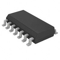


 工商网监
湘ICP备2023018690号
工商网监
湘ICP备2023018690号

