www.fairchildsemi.com
MC78TXX
3-Terminal 3A Positive Voltage Regulator
Features
• • • • • • • • Output Current in Excess of 3.0A Output Transistor Safe Operating Area Compensation Power Dissipation :25W Internal Short Circuit Current Limiting Internal Thermal Overload Protection Output Voltage Offered in 4% Tolerance No External Components Required Output Voltage of 5,12 and 15V
Description
This family of fixed voltage regulators are monolithic integrated circuit capable of driving loads in excess of 3.0 A.
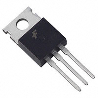
TO-220
GND
1
1.Input 2. GND 3. Output
Internal Block Diagram
INPUT 1 CURRENT GENERATOR
SERIES PASS ELEMENT
OUTPUT 3
SOA PROTECTION
STARTING CIRCUIT
REFERENCE VOLTAGE
ERROR AMPLIFIER
THERMAL PROTECTION
GND 2
Rev. 1.0.1
©2002 Fairchild Semiconductor Corporation
�MC78TXX
Absolute Maximum Ratings
Parameter Input Voltage (for VO = 5V to 12V) (for VO = 15V) Power Dissipation Thermal Resistance, Junction to Air (Note1, 2) Ta = +25°C Thermal Resistance, Junction to Case (Note1) Tc = +25°C Operating Junction Temperature Range Storage Temperature Range
Note: 1. Thermal resistance test board Size: 76.2mm * 114.3mm * 1.6mm(1S0P) JEDEC standard: JESD51-3, JESD51-7 2. Assume no ambient airflow.
Symbol VI PD RθJA RθJC TJ TSTG
Value 35 40 Internally limited 65 2.5 0 ~ +125 -65 ~ +150
Unit V V
°C/W °C/W °C °C
Electrical Characteristics(MC78T05)
(VI = 10V, IO = 3.0 A, 0°C ≤ TJ ≤ +125°C, Po ≤ PMAX (Note3), unless otherwise specified. ) Parameter Output Voltage Symbol Vo Conditions 5mA ≤ Io ≤ 3.0A , TJ = +25°C 7.3V ≤ VI ≤ 20V, 5mA ≤ Io ≤ 2.0A 7.2V ≤ VI ≤ 35V , Io=5mA, TJ =+25°C 7.2V ≤ VI ≤ 35V , Io=1.0A, TJ = +25°C 7.5V ≤ VI ≤ 20V, Io =2.0A, TJ = +25°C 8.0V ≤ VI ≤ 12V, Io =3.0A, TJ = +25°C 5mA ≤ Io ≤ 3.0A , TJ = +25°C 5mA ≤ Io ≤ 3.0A Pulse =10ms, P = 20W TA = +25°C 5mA ≤ Io ≤ 3.0A , TJ = +25°C 5mA ≤ Io ≤ 3.0A 7.2V ≤ VI ≤ 35V, Io = 5mA TJ = +25°C ; 7.5V ≤ VI ≤ 20V, Io =2.0A ; 5mA ≤ Io ≤ 3.0A, TJ = +25°C f = 120Hz, 8V ≤ VI ≤ 18V, Io = 2.0A TJ = +25°C Io = 3A ,TJ = +25°C TA = +25°C, 10Hz ≤ f ≤ 100kHz TA = +25°C f = 1.0kHz VI = 35V, TJ =+25°C Io = 5.0mA Min. 4.8 4.75 Typ. 5.0 5.0 3.0 10 15 0.002 3.5 4.0 0.1 Max. 5.2 5.25 25 30 80 0.03 5.0 6.0 0.8 Unit V
Line Regulation (Note4)
∆VO
mV mV mV %Vo/W mA mA mA
Load Regulation (Note4) Thermal Regulation Quiescent Current
∆VO REGT IQ
-
Quiescent Current Change
∆ IQ
-
Ripple Rejection Dropout Voltage Output Noise Voltage Peak Output Current Output Resistance Short Circuit Current Limit
RR VD VN IPK Ro Isc
-
75 2.2 10 5.0 2.0 1.5 0.2
2.5 2.5 -
dB V µV/Vo A mΩ A mV/°C
Average Temperature ∆VO/∆T Coefficient of Output Voltage
Note:
3. Although power dissipation is internally limited, specifications apply only for PO ≤ Pmax, Pmax = 25W 4. Load and line regulation are specified at constant junction temperature. Change in Vo due heating effects must be taken into account separately. Pulse testing with low duty is used.
2
�MC78TXX
Electrical Characteristics(MC78T12) (Continued)
(VI = 19V, IO = 3.0 A, 0°C ≤ TJ ≤ +125°C, Po ≤ PMAX (Note1), unless otherwise specified. ) Parameter Output Voltage Symbol Vo Conditions 5mA ≤ Io ≤ 3.0A , TJ =+25°C 14.5V ≤ VI ≤ 27V, 5mA ≤ Io ≤ 2.0A 14.5V ≤ VI ≤ 35V, Io=5mA, TJ =+25°C 14.5V ≤ VI ≤ 35V, Io=1.0A, TJ =+25°C 14.9V ≤ VI ≤ 28V, Io =2.0A, TJ =+25°C 16V ≤ VI ≤ 22V, Io =3.0A, TJ =+25°C 5mA ≤ Io ≤ 3.0A, TJ =+25°C 5mA ≤ Io ≤ 3.0A Pulse =10ms, P = 20W TA = +25°C 5mA ≤ Io ≤ 3.0A, TJ =+25°C 5mA ≤ Io ≤ 3.0A 14.5V ≤ VI ≤ 35V, Io = 5mA TJ =+25°C ; 14.9V ≤ VI ≤ 27V, Io =2.0A ; 5mA ≤ Io ≤ 3.0A, TJ =+25°C f = 120Hz, 15V ≤ VI ≤ 25V, Io = 2.0A TJ =+25°C Io = 3A,TJ =+25°C TA =+25°C, 10Hz ≤ f ≤ 100kHz TA =+25°C f = 1.0kHz VI = 35V, TJ =+25°C Io = 5.0mA Min. 11.5 11.4 Typ. 12 12 6.0 10 15 0.002 3.5 4.0 0.1 Max. 12.5 12.8 45 30 80 0.03 5.0 6.0 0.8 Unit V
Line Regulation (Note2)
∆VO
mV mV mV %Vo/W mA mA mA
Load Regulation (Note2) Thermal Regulation Quiescent Current
∆VO REGT IQ ∆ IQ
-
Quiescent Current Change
-
Ripple Rejection Dropout Voltage Output Noise Voltage Peak Output Current Output Resistance Short Circuit Current Limit
RR VD VN IPK Ro Isc
-
67 2.2 10 5.0 2.0 1.5 0.5
2.5 2.5 -
dB V µV/Vo A mΩ A mV/°C
Average Temperature ∆VO/∆T Coefficient of Output Voltage
Note: 1. Although power dissipation is internally limited, specifications apply only for PO ≤ Pmax, Pmax = 25W 2. Load and line regulation are specified at constant junction temperature. Change in Vo due heating effects must be taken into account separately. Pulse testing with low duty is used. ( PMAX = 25W)
3
�MC78TXX
Electrical Characteristics(MC78T15) (Continued)
(VI = 23V, IO = 3.0 A, 0°C ≤ TJ ≤ +125°C, Po ≤ PMAX (Note1), unless otherwise specified. ) Parameter Output Voltage Symbol Vo Conditions 5mA ≤ Io ≤ 3.0A, TJ =+25°C 17.5V ≤ VI ≤ 30V, 5mA ≤ Io ≤ 2.0A 17.6V ≤ VI ≤ 40V, Io=5mA, TJ =+25°C 17.6V ≤ VI ≤ 40V, Io=1.0A, TJ =+25°C 18V ≤ VI ≤ 30V, Io =2.0A, TJ =+25°C 20V ≤ VI ≤ 26V, Io =3.0A, TJ =+25°C 5mA ≤ Io ≤ 3.0A, TJ =+25°C 5mA ≤ Io ≤ 3.0A Pulse =10ms, P = 20W TA = +25°C 5mA ≤ Io ≤ 3.0A, TJ =+25°C 5mA ≤ Io ≤ 3.0A 17.6V ≤ VI ≤ 40V, Io = 5mA TJ =+25°C ; 18V ≤ VI ≤ 30V, Io =2.0A ; 5mA ≤ Io ≤ 3.0A, TJ =+25°C f = 120Hz, 18.5V ≤ VI ≤ 28.5V, Io = 2.0A TJ =+25°C Io = 3A ,TJ = +25°C TA = +25°C, 10Hz ≤ f ≤ 100kHz TA = +25°C f = 1.0kHz VI = 40V, TJ = +25°C Io = 5.0mA Min. 14.4 14.25 Typ. 15 15 7.5 10 15 0.002 3.5 4.0 0.1 Max. 15.6 15.75 55 30 80 0.03 5.0 6.0 0.8 Unit V
Line Regulation (Note2)
∆VO
mV mV mV %Vo/W mA mA mA
Load Regulation (Note2) Thermal Regulation Quiescent Current
∆VO REGT IQ ∆ IQ
-
Quiescent Current Change
-
Ripple Rejection Dropout Voltage Output Noise Voltage Peak Output Current Output Resistance Short Circuit Current Limit
RR VD VN IPK Ro Isc
-
65 2.2 10 5.0 2.0 1.0 0.5
2.5 2.0 -
dB V µV/Vo A mΩ A mV/°C
Average Temperature ∆VO/∆T Coefficient of Output Voltage
Note: 1. Although power dissipation is internally limited, specifications apply only for PO ≤ Pmax, Pmax = 25W 2. Load and line regulation are specified at constant junction temperature. Change in Vo due heating effects must be taken into account separately. Pulse testing with low duty is used. ( PMAX = 25W)
4
�MC78TXX
Typical Application
INPUT 1 KA78TXX MC78TXX 2 3 OUTPUT
0.33 µF
0. 1 µF
Note: 1. To specify an output voltage, substitute voltage value for “XX”. 2. Bypass Capacitors are recommend for optimum stability and transient response and should be located as close as possible to the regulator
5
�MC78TXX
Mechanical Dimensions
Package Dimensions in millimeters
TO-220
9.90 ±0.20 4.50 ±0.20
1.30 ±0.10
2.80 ±0.10
(8.70) ø3.60 ±0.10
(1.70)
1.30 –0.05
+0.10
9.20 ±0.20
(1.46)
13.08 ±0.20
(1.00)
(3.00)
15.90 ±0.20
1.27 ±0.10
1.52 ±0.10
0.80 ±0.10 2.54TYP [2.54 ±0.20] 2.54TYP [2.54 ±0.20]
10.08 ±0.30
18.95MAX.
(3.70)
(45° )
0.50 –0.05
+0.10
2.40 ±0.20
10.00 ±0.20
6
�MC78TXX
Ordering Information
Product Number MC78T05CT MC78T12CT MC78T15CT TO-220 0 ~ +125°C Package Operating Temperature
7
�MC78TXX
DISCLAIMER FAIRCHILD SEMICONDUCTOR RESERVES THE RIGHT TO MAKE CHANGES WITHOUT FURTHER NOTICE TO ANY PRODUCTS HEREIN TO IMPROVE RELIABILITY, FUNCTION OR DESIGN. FAIRCHILD DOES NOT ASSUME ANY LIABILITY ARISING OUT OF THE APPLICATION OR USE OF ANY PRODUCT OR CIRCUIT DESCRIBED HEREIN; NEITHER DOES IT CONVEY ANY LICENSE UNDER ITS PATENT RIGHTS, NOR THE RIGHTS OF OTHERS. LIFE SUPPORT POLICY FAIRCHILD’S PRODUCTS ARE NOT AUTHORIZED FOR USE AS CRITICAL COMPONENTS IN LIFE SUPPORT DEVICES OR SYSTEMS WITHOUT THE EXPRESS WRITTEN APPROVAL OF THE PRESIDENT OF FAIRCHILD SEMICONDUCTOR CORPORATION. As used herein: 1. Life support devices or systems are devices or systems which, (a) are intended for surgical implant into the body, or (b) support or sustain life, and (c) whose failure to perform when properly used in accordance with instructions for use provided in the labeling, can be reasonably expected to result in a significant injury of the user.
www.fairchildsemi.com 11/12/02 0.0m 001 Stock#DSxxxxxxxx 2002 Fairchild Semiconductor Corporation
2. A critical component in any component of a life support device or system whose failure to perform can be reasonably expected to cause the failure of the life support device or system, or to affect its safety or effectiveness.
�


 工商网监
湘ICP备2023018690号
工商网监
湘ICP备2023018690号
