Product Specification
4.25 Gb/s RoHS Compliant Short-Wavelength 2x7 SFF Transceiver
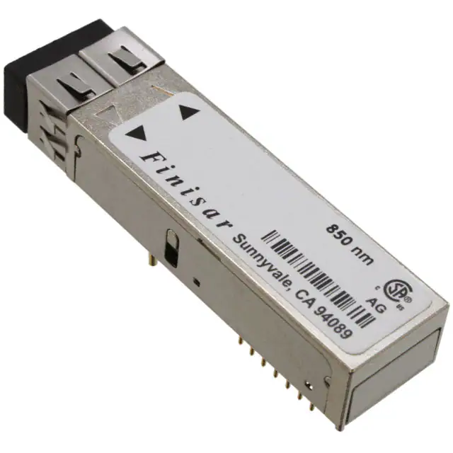
FTLF8524E2xNy
PRODUCT FEATURES Up to 4.25 Gb/s bi-directional data links 2x7 pin SFF-like footprint Built-in digital diagnostic functions 850nm Oxide VCSEL laser transmitter Duplex LC connector RoHS Compliant and Lead Free Up to 500m on 50/125µm MMF, 300m on 62.5/125µm MMF Metal enclosure, for lower EMI Single 3.3V power supply Extended operating temperature range: -10°C to 85°C Finisar’s FTLF8524E2xNy Small Form Factor (SFF) transceivers comply with the 2x5 standard package defined by the Small Form Factor Multi-Sourcing Agreement (MSA)1, with the exception of 4 extra pins outlined in Section I below. They are compatible with Fibre Channel FC-PI-2 Rev. 7.02 and are RoHS compliant and lead-free per Directive 2002/95/EC3 and Finisar Application Note AN-2038. PRODUCT SELECTION APPLICATIONS Tri-Rate 1.063/2.125/4.25 Gb/s Fibre Channel
FTLF8524E2xNy
x y G K L V 2 Grounding Pins, Short EMI shield 2 Grounding Pins, Long EMI shield Non Rate Selectable - 1x, 2x, 4x Fibre Channel Rate Selectable - 1x, 2x, 4x Fibre Channel
Finisar Corporation July 12, 2005 RevG
Page 1
�FTLF8524E2xNy 2x7 Pin SFF Product Specification – July 2005
I.
Pin MS 1 2 3 4 5 6 7 8 9 10 A B C D Notes:
Pin Descriptions
Symbol MS VEER VCCR SD RDRD+ VCCT VEET TDIS TD+ TDSDA SCL Rate Select Reserved Name/Description Mounting Studs are for mechanical attachment and are connected to chassis ground. Chassis ground is internally isolated from circuit grounds. Connection to user’s ground plane is recommended. Receiver Ground (Common with Transmitter Ground) Receiver Power Supply Signal Detect. Logic 1 indicates normal operation. Receiver Inverted DATA out. AC Coupled Receiver Non-inverted DATA out. AC Coupled Transmitter Power Supply Transmitter Ground (Common with Receiver Ground) Transmitter Disable Transmitter Non-Inverted DATA in. AC Coupled. Transmitter Inverted DATA in. AC Coupled Two Wire Digital Diagnostics Data Interface Two Wire Digital Diagnostics Clock Interface 1.063 Gb/s or 2.125 Gb/s Fibre Channel, Open or Low = (Low Bandwidth) 2.125 or 4.25 Gb/s Fibre Channel (High Bandwidth) High = Logic Family NA NA NA LVTTL See Rx spec. See Rx spec. NA NA LVTTL See Tx spec. See Tx spec. See Note 1 See Note 1 LVTTL See Note 2 NA
1. Should be pulled up with 4.7k – 10kohms on host board to a voltage between 2.0V and VCC. 2. For Rate Selectable version only: In accordance with SFF Committee SFF-8079 Draft Rev. 1.6,
Table 3. Note that rate select can also be set through 2-wire bus in accordance with SFF-84725 at Bit 3, Byte 110, Address A2h (note: writing ‘1’ selects full bandwidth operation). Rate select is the logic OR of the input state of Rate Select Pin and 2-wire bus. Non Rate Selectable version can operate at 1x, 2x, 4x Fibre Channel independent of rate select pin setting.
MS
D B 10 …
6
TOP VIEW
CA1 … 5
MS
Finisar Corporation July 12, 2005 RevG
Page 2
�FTLF8524E2xNy 2x7 Pin SFF Product Specification – July 2005
II.
Absolute Maximum Ratings
Symbol Vcc TS TOP RH Min -0.5 -40 -10 0 Typ Max 4.0 85 85 85 260/10 260/10 Unit V °C °C % °C/s °C/s Ref.
Parameter Maximum Supply Voltage Storage Temperature Case Operating Temperature Relative Humidity Hand Lead Soldering Temperature/Time Wave Lead Soldering Temperature/Time Notes: 1. Non condensing.
1
III.
Electrical Characteristics (TOP = -10 to 85 °C, VCC = 3.0 to 3.6 Volts)
Symbol Vcc Icc Rin Vin,pp VD VEN Rout Vout,pp tr/ tf SD normal SD fault PSR RX ∆ DJ RX ∆ DJ RX ∆ TJ RX ∆ TJ Min 3.0 Typ 180 80 250 2 Vee 80 250 100 Max 3.6 240 120 1200 Vcc Vee+ 0.8 120 550 120 VccHOST Vee+0.5 100 51.7 23.5 122.4 61 Unit V mA Ω mV V V Ω mV ps V V mVpp ps ps ps ps Ref.
Parameter Supply Voltage Supply Current Transmitter Input differential impedance Single ended data input swing Transmit Disable Voltage Transmit Enable Voltage Receiver Output differential impedance Single ended data output swing Data output rise/fall time Mask Margin ≤ 2.125 Gb/s Signal Detect Normal Signal Detect Fault Power Supply Rejection Deterministic Jitter Contribution @ 2.125 Gb/s Deterministic Jitter Contribution @ 4.25 Gb/s Total Jitter Contribution (p-p) @ 2.125 Gb/s Total Jitter Contribution (p-p) @ 4.25 Gb/s
1
2 1 3 4 5 5 6 7 7 8 8
100 350 45%
Vee
Notes: 1. AC coupled. 2. Or open circuit. 3. Into 100 Ω differential termination. Data pattern is PRBS 27-1. 4. 20 – 80 %. 5. Signal detect is LVTTL. Logic 1 indicates normal operation; logic 0 indicates no signal detected. 6. All transceiver specifications are compliant with a power supply sinusoidal modulation of 20 Hz to 1.5 MHz up to specified value applied through the power supply filtering network shown on page 23 of the Small Form-factor Pluggable (SFP) Transceiver MultiSource Agreement (MSA), September 14, 2000. 7. Measured with DJ-free data input signal. In actual application, output DJ will be the sum of input DJ and ∆ DJ, 10-12 BER. 8. If measured with TJ-free data input signal, , 10-12 BER. In actual application, output TJ will be given by:
TJ OUT = DJ IN + ∆DJ +
(TJ IN
− DJ IN ) + (∆TJ − ∆DJ )
2
2
Finisar Corporation July 12, 2005 RevG
Page 3
�FTLF8524E2xNy 2x7 Pin SFF Product Specification – July 2005
IV.
Optical Characteristics (TOP = -10 to 85 °C, VCC = 3.0 to 3.6 Volts)
Symbol POUT λ σ OMA OMA OMA tr/ tf RIN TX ∆ DJ TX ∆ DJ TX ∆ TJ TX ∆ TJ RxSENS RxSENS RxSENS 0.055 0.096 0.138 RxMAX λC RL SD normal SD fault 770 12 -30 0.5 0 1500 2500 860 -20 Min -9 830 247 196 156 90 -118 56.5 28.2 119 56.5 45% -20 -18 -15 dBm dBm dBm mW mW mW dBm MHz MHz nm dB dBm dBm dB 6 6 6 8 8 8 9 10 Typ Max -2.5 860 0.85 Unit dBm nm nm µW µW µW ps dB/Hz ps ps ps ps Ref. 1
Parameter Transmitter Output Opt. Pwr: 50 or 62.5 MMF Optical Wavelength Spectral Width Optical Modulation Amplitude @ 4.25 Gb/s Optical Modulation Amplitude @ 2.125 Gb/s Optical Modulation Amplitude @ 1.0625 Gb/s Optical Rise/Fall Time Relative Intensity Noise Deterministic Jitter Contribution @ 2.125 Gb/s Deterministic Jitter Contribution @ 4.25 Gb/s Total Jitter Contribution @ 2.125 Gb/s Total Jitter Contribution @ 4.25 Gb/s Mask Margin ≤ 2.125 Gb/s Receiver Receiver Sensitivity = 1.0625 Gb/s Receiver Sensitivity = 2.125 Gb/s Receiver Sensitivity = 4.25 Gb/s Stressed RX sens. =1.0625 Gb/s Stressed RX sens. =2.125 Gb/s Stressed RX sens. =4.25 Gb/s Average Received Power Receiver Elec. 3 dB cutoff frequency Receiver Elec. 3 dB cutoff frequency Optical Center Wavelength Return Loss Signal Detect Normal Signal Detect Fault Signal Detect Hysteresis
2 2 2 3 4 4 5 5
Notes: 1. Class 1 Laser Safety per FDA/CDRH, EN (IEC) 60825 laser safety regulations. 2. Equivalent extinction ratio specification for Fibre Channel. Allows smaller ER at higher average power. 3. Unfiltered, 20-80%. Complies with FC 1x and 2x eye mask when filtered. 4. Measured with DJ-free data input signal. In actual application, output DJ will be the sum of input DJ and ∆ DJ, 10-12 BER. 5. If measured with TJ-free data input signal, 10-12 BER. In actual application, output TJ will be given by:
TJ OUT = DJ IN + ∆DJ +
6. 7. 8. 9. 10.
(TJ IN
− DJ IN ) + (∆TJ − ∆DJ )
2
2
Specifications are for 50 micro-meter or 62.5 micro-meter fiber As measured with 9dB extinction ratio. Measured with conformance signals defined in FC-PI-2 Rev. 7.0 specifications. Rate selectable version in low bandwidth mode. Rate selectable version in high bandwidth mode.
Finisar Corporation July 12, 2005 RevG
Page 4
�FTLF8524E2xNy 2x7 Pin SFF Product Specification – July 2005
V.
General Specifications
Parameter Symbol BR BER L L Min Typ 1.062, 2.125, 4.25 Max Units Gb/sec Ref. 1 5 2 3 4 2 3 4
Data Rate Bit Error Rate Fiber Length on 50/125µm MMF Fiber Length on 62.5/125µm MMF
10-12 550 300 150 300 150 70
m m
Notes: 1. 1x, 2x, and 4x Fibre Channel compatible per FC-PI-2 Rev. 7.0. 2. At 1.0625 Gb/s Fibre Channel data rate. 3. At 2.125 Gb/s Fibre Channel data rate. 4. At 4.25 Gb/s Fibre Channel data rate. 5. At 1.0625, 2.125, and 4.25Gb/s with PRBS 27-1.
VI.
Environmental Specifications
Finisar SFF transceivers have an extended operating temperature range from –10°C to +85°C case temperature.
Parameter Case Operating Temperature Storage Temperature Symbol Top Tsto Min -10 -40 Typ Max 85 85 Units °C °C Ref.
Notes: 1. SFF transceivers may be water washed with the optical port plug in position. However, the process must be followed by a baking step at 80°C for one hour, to ensure the drying of any water which may be trapped inside then shells of the modules.
VII.
Regulatory Compliance
Finisar transceivers are Class 1 Laser Products and comply with US FDA regulations. These products are certified by TÜV and CSA to meet the Class 1 eye safety requirements of EN (IEC) 60825 and the electrical safety requirements of EN (IEC) 60950. Copies of certificates are available at Finisar Corporation upon request.
Finisar Corporation July 12, 2005 RevG
Page 5
�FTLF8524E2xNy 2x7 Pin SFF Product Specification – July 2005
VIII. Digital Diagnostic Functions Finisar FTLF8524E2xNy 2x7 SFF transceivers support a 2-wire serial communication protocol. This interface is identical to the 2-wire serial interface defined in the SFP MSA4, however in this case it is implemented on the 2x7 SFF form factor. The standard SFP serial ID provides access to identification information that describes the transceiver’s capabilities, standard interfaces, manufacturer, and other information. Additionally, an enhanced digital diagnostic monitoring interface is defined, which allows real-time access to device operating parameters such as transceiver temperature, laser bias current, transmitted optical power, received optical power and transceiver supply voltage. It also defines a sophisticated system of alarm and warning flags, which alerts end-users when particular operating parameters are outside of a factory set normal range. In order to access the identification information, the 2x7 SFF transceivers have a 256byte memory map in E2PROM that is accessible over a 2-wire serial interface at the 8 bit address 1010000X (A0h). The digital diagnostic monitoring interface makes use of the 8 bit address 1010001X (A2h), so the originally defined serial ID memory map remains unchanged. The interface is identical to, and is thus fully backward compatible with both the GBIC Specification and the SFP Multi Source Agreement. Additional information, including details of the electronic interface, is described in Finisar Application Note AN2030: “Digital Diagnostics Monitoring Interface for SFP Optical Transceivers”. The operating and diagnostics information is monitored and reported by a Digital Diagnostics Transceiver Controller (DDTC) inside the transceiver, which is accessed through a 2-wire serial interface. When the serial protocol is activated, the serial clock signal (SCL, Mod Def 1) is generated by the host. The positive edge clocks data into the 2x7 SFF transceiver into those segments of the E2PROM that are not write-protected. The negative edge clocks data from the 2x7 SFF transceiver. The serial data signal (SDA, Mod Def 2) is bi-directional for serial data transfer. The host uses SDA in conjunction with SCL to mark the start and end of serial protocol activation. The memories are organized as a series of 8-bit data words that can be addressed individually or sequentially. For more information, please see the SFP MSA documentation4,5 and Finisar Application Note AN-2030. One difference in the implementation of digital diagnostics in the SFF 2x7 form factor from the SFP MSA documentation is the readout of Bit 1, Byte 110 at Address A2h (called “Digital State of the LOS output pin” in the SFP documentation). In the SFF 2x7, the output of this bit is inverted to indicate Signal Detect and match the output of the Signal Detect pin on the SFF part. Digital diagnostics for the FTLF8524E2xNy can be used in host systems that require either internally or externally calibrated digital diagnostics.
Finisar Corporation July 12, 2005 RevG Page 6
�FTLF8524E2xNy 2x7 Pin SFF Product Specification – July 2005
IX.
Mechanical Specifications
Finisar’s Small Form Factor (SFF) transceivers comply with the standard dimensions defined by the Small Form Factor Multi-Sourcing Agreement (MSA).
FTLF8524E2GNy
Finisar Corporation July 12, 2005 RevG
Page 7
�FTLF8524E2xNy 2x7 Pin SFF Product Specification – July 2005
FTLF8524E2KNy
Finisar Corporation July 12, 2005 RevG
Page 8
�FTLF8524E2xNy 2x7 Pin SFF Product Specification – July 2005
X.
PCB Layout and Bezel Recommendations
Minimum Recommended Pitch is 0.600”
Finisar Corporation July 12, 2005 RevG
Page 9
�FTLF8524E2xNy 2x7 Pin SFF Product Specification – July 2005
XI.
References
1. Small Form Factor (SFF) Transceiver Multi-source Agreement (MSA). July 5, 2000. 2. “Fibre Channel Draft Physical Interface Specification (FC-PI-2 Rev. 7.0)”. American National Standard for Information Systems. 3. Directive 2002/95/EC of the European Council Parliament and of the Council, “on the restriction of the use of certain hazardous substances in electrical and electronic equipment.” January 27, 2003. 4. Small Form-factor Pluggable (SFP) Transceiver Multi-source Agreement (MSA), September 14, 2000. 5. “Digital Diagnostics Monitoring Interface for Optical Transceivers”. SFF Document Number SFF-8472, Revision 9.3. XII. For More Information
Finisar Corporation 1308 Moffett Park Drive Sunnyvale, CA 94089-1133 Tel. 1-408-548-1000 Fax 1-408-541-6138 sales@finisar.com www.finisar.com
Finisar Corporation July 12, 2005 RevG
Page 10
�


 工商网监
湘ICP备2023018690号
工商网监
湘ICP备2023018690号
