SMD Switching Diode
BAL99/BAV99/BAW56/BAV70
Formosa MS
List
List................................................................................................. 1
Package outline............................................................................... 2
Features.......................................................................................... 2
Mechanical data............................................................................... 2
Maximum ratings ............................................................................. 2
Thermal Characteristics ................................................................... 3
Electrical Characteristics.................................................................. 3
Rating and characteristic curves........................................................ 4
Pinning information...........................................................................5
Marking........................................................................................... 5
Suggested solder pad layout............................................................. 5
Packing information.......................................................................... 6
Reel packing.................................................................................... 7
Suggested thermal profiles for soldering processes............................. 7
High reliability test capabilities...........................................................8
http://www.formosams.com/
TEL:886-2-22696661
FAX:886-2-22696141
Page 1
Document ID
Issued Date
Revised Date
Revision
DS-221906
2008/02/10
2010/11/29
C
Page.
8
�Formosa MS
SMD Switching Diode
BAL99/BAV99/BAW56/BAV70
225mW Surface Mount
Switching Diode- 70V
Features
Package outline
• Fast speed switching.
• For general purpose switching application.
• High conductance.
• Silicon epitaxial planar chip.
• Lead-free parts meet RoHS requirments.
• Suffix "-H" indicates Halogen-free part, ex.BAL99-H.
(B)
(C)
(A)
0.063 (1.60)
Mechanical data
0.012 (0.30)
0.034 (0.85)
0.020 (0.50)
.084(2.10)
.068(1.70)
0.110 (2.80)
0.120 (3.04)
0.045 (1.15)
SOT-23
0.027 (0.67)
0.013 (0.32)
0.047 (1.20)
0.108 (2.75)
• Epoxy:UL94-V0 rated flame retardant
• Case : Molded plastic, SOT-23
• Terminals : Solder plated, solderable per
0.051 (1.30)
0.003 (0.09)
0.007 (0.18)
0.083 (2.10)
0.035 (0.89)
MIL-STD-750, Method 2026
• Mounting Position : Any
• Weight : Approximated 0.008 gram
Dimensions in inches and (millimeters)
Maximum ratings (AT T =25 C unless otherwise noted)
o
A
PARAMETER
SYMBOL
Reverse Voltage
BAL99
BAV99
VR
BAV70
BAW56
UNIT
V
70
Forward Current
IF
Peak Forward Surge Current
I FM
500
mA
Non-Repetitive Peak Forward Surge Current
@ t=1.0us
@ t=1.0s
I FSM
2.0
1.0
A
SYMBOL
MAX.
UNIT
100
215
mA
200
Thermal Characteristics
PARAMETER
Total Device Dissipation FR-5
1
O
Board* , T A = 25 C
Total Device Dissipation Alumina
mW/ OC
1.8
Thermal Resistance Junction to Ambient
R θJA
2
mW
225
PD
Derate Above 25 OC
Substrate* , T A = 25 C
Derate Above 25 OC
O
556
O
mW
300
PD
C/W
mW/ OC
2.4
Thermal Resistance Junction to Ambient
R θJA
417
Operating Junction Temperature Range
TJ
-55 ~ +150
o
C
-55 ~ +150
o
C
Storage Temperature Range
T STG
O
1. FR-5 = 1.0 x 0.75 x 0.062 in.
2. Alumina = 0.4 x 0.3 x 0.024 in. 99.5% alumina.
http://www.formosams.com/
TEL:886-2-22696661
FAX:886-2-22696141
Page 2
Document ID
Issued Date
Revised Date
Revision
DS-221906
2008/02/10
2010/11/29
C
Page.
8
C/W
�Formosa MS
SMD Switching Diode
BAL99/BAV99/BAW56/BAV70
Electrical Characteristics (AT T =25 C unless otherwise noted)
o
A
PARAMETER
SYMBOL
MIN.
V BR
70
Reverse Breakdown Voltage(I BR=100uAdc)
Reverse Voltage Leakage Current
(at V R = 70V, T J =25 OC)BAL99/BAV99/BAW56/BAV70
(at V R = 25V, T J =150 OC)BAL99/BAV99/BAW56
(at V R = 25V, T J =150 OC)BAV70
(at V R = 70V, T J =150 OC)BAL99/BAV99/BAW56
(at V R = 70V, T J =150 OC)BAV70
CD
Reverse Recovery Time(I F = I R = 10mA,V R = 5.0Vdc,
I R(REC) = 1.0mAdc, R L = 100 OHM)
Forward Voltage
(at I F = 1.0mAdc)
(at I F = 10mAdc)
(at I F = 50mAdc)
(at I F = 150mAdc)
V
2.5
30
60
50
100
IR
Diode Capacition(V R = 0V, f = 1.0MHz)
BAL99/BAV99/BAV70
BAW56
UNIT
MAX.
µA
1.5
2.0
pF
t rr
6.0
ns
VF
715
855
1000
1250
mV
Recovery Time Equivalent Test Circuit
820 OHM
+10V
2K
100uH
0.1 uF
IF
tr
tp
t
IF
0.1 uF
t
t rr
10%
DUT
50 OHM OUTPUT
PULSE
GENERATOR
50 OHM INPUT
SAMPLING
OSCILLOSCOPE
90%
VR
IR(REC)=1 mA
IR
OUTPUT PULSE
(IF=IR=10mA;measured
at IR(REC)=1mA)
Notes : 1. A2.0 Kohm variable resistor adjusted for a forward Current (IF) of 10mA.
Notes:
Notes:
2. Input pulse is adjusted so IR(peak) is equal to 10 mA.
3. tp >> trr.
http://www.formosams.com/
TEL:886-2-22696661
FAX:886-2-22696141
Page 3
Document ID
Issued Date
Revised Date
Revision
DS-221906
2008/02/10
2010/11/29
C
Page.
8
�Rating and characteristic curves for each diode (BAL99/BAV99/BAW56/BAV70)
FIG.2 - TYPICAL REVERSE
FIG.1-TYPICAL FORWARD
CHARACTERISTICS
T J=150°C
T J=85°C
T J=25°C
REVERSE CURRENT, (uA)
INSTANTANEOUS FORWARD CURRENT,(mA)
CHARACTERISTICS
T J=125°C
T J=85°C
T J=55°C
T J=-40°C
T J=25°C
FORWARD VOLTAGE,(V)
REVERSE VOLTAGE,(V)
FIG.3b - TYPICAL DIODE CAPACITANCE
BAW56
DIODE CAPACITANCE,(pF)
DIODE CAPACITANCE,(pF)
FIG.3a - TYPICAL DIODE CAPACITANCE
BAL99/BAV99/BAV70
REVERSE VOLTAGE,(V)
http://www.formosams.com/
TEL:886-2-22696661
FAX:886-2-22696141
REVERSE VOLTAGE,(V)
Page 4
Document ID
Issued Date
Revised Date
Revision
DS-221906
2008/02/10
2010/11/29
C
Page.
8
�Formosa MS
SMD Switching Diode
BAL99/BAV99/BAW56/BAV70
Pinning information
Type number
Simplified outline
Marking code
(A)
BAL99
(B)
Symbol
A
L4, A6,JF
(C)
(A)
BAV99
C
(B)
A
(B)
A
(C)
C
B
JC, A1
(C)
(A)
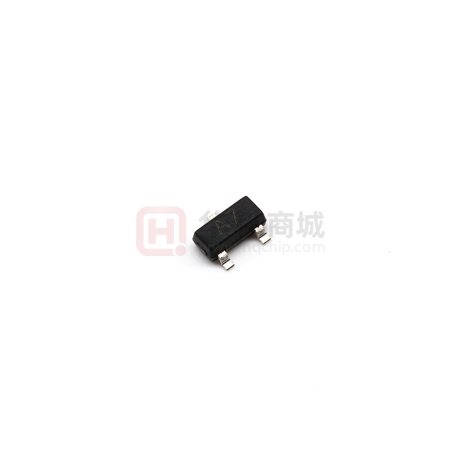
BAV70
B
JG, A7
(A)
BAW56
B
C
(B)
A
B
JA, A4
C
(C)
Suggested solder pad layout
SOT-23
0.037(0.95)
0.037(0.95)
0.079(2.0)
0.035(0.90)
0.031(0.80)
Dimensions in inches and (millimeters)
http://www.formosams.com/
TEL:886-2-22696661
FAX:886-2-22696141
Page 5
Document ID
Issued Date
Revised Date
Revision
DS-221906
2008/02/10
2010/11/29
C
Page.
8
�Formosa MS
SMD Switching Diode
BAL99/BAV99/BAW56/BAV70
Packing information
P0
P1
d
E
F
B
A
W
P
D2
D1
T
C
W1
D
unit:mm
Item
Symbol
Tolerance
SOT-23
Carrier width
Carrier length
Carrier depth
Sprocket hole
13" Reel outside diameter
13" Reel inner diameter
7" Reel outside diameter
7" Reel inner diameter
Feed hole diameter
Sprocket hole position
Punch hole position
Punch hole pitch
Sprocket hole pitch
Embossment center
Overall tape thickness
Tape width
Reel width
A
B
C
d
D
D1
D
D1
D2
E
F
P
P0
P1
T
W
W1
0.1
0.1
0.1
0.1
2.0
min
2.0
min
0.5
0.1
0.1
0.1
0.1
0.1
0.1
0.3
1.0
3.15
2.77
1.22
1.50
178.00
62.00
13.00
1.75
3.50
4.00
4.00
2.00
0.23
8.00
11.40
Note:Devices are packed in accor dance with EIA standar RS-481-A and specifications listed above.
http://www.formosams.com/
TEL:886-2-22696661
FAX:886-2-22696141
Page 6
Document ID
Issued Date
Revised Date
Revision
DS-221906
2008/02/10
2010/11/29
C
Page.
8
�SMD Switching Diode
BAL99/BAV99/BAW56/BAV70
Formosa MS
Reel packing
PACKAGE
SOT-23
REEL SIZE
7"
REEL
(pcs)
COMPONENT
SPACING
(m/m)
BOX
(pcs)
3000
4.0
30,000
REEL
DIA,
(m/m)
INNER
BOX
(m/m)
183*183*123
CARTON
SIZE
(m/m)
178
382*262*387
CARTON
(pcs)
APPROX.
GROSS WEIGHT
(kg)
11.6
240,000
Suggested thermal profiles for soldering processes
1.Storage environment: Temperature=5 oC ~40 oC Humidity=55%±25%
2.Reflow soldering of surface-mount devices
Critical Zone
TL to TP
Tp
TP
Ramp-up
TL
TL
Tsmax
Temperature
Tsmin
tS
Preheat
Ramp-down
25
t25o C to Peak
Time
3.Reflow soldering
Profile Feature
Soldering Condition
Average ramp-up rate(T L to T P )
o
很抱歉,暂时无法提供与“BAV99”相匹配的价格&库存,您可以联系我们找货
免费人工找货- 国内价格
- 50+0.06661
- 150+0.05686
- 1000+0.04712
- 5000+0.04322


 工商网监
湘ICP备2023018690号
工商网监
湘ICP备2023018690号

