Chipi-X Cable Datasheet
Version 1.1
Document Reference No.: FT_000634
Clearance No.: FTDI# 288
Future Technology
Devices International
Ltd
Datasheet
Chipi-X Cable
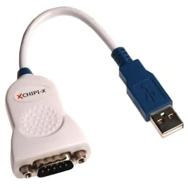
Chipi-X is a USB to full-handshake RS232 cable with a male DB9 connector. This cable is
available with or without an enclosure.
1
Introduction
The Chipi-X cable is a USB to RS232 level full-handshake UART cable. Chipi-X utilises FTDI’s
FT231XS USB to full-handshake UART IC and FT3243S RS232 transceiver IC. A male DB9 (aka
DE9) connector provides the connectivity for RS232 communications and a USB-A plug tethered
by a 10cm cable to the PCB provides connectivity for USB communications.
All components used are Pb-free (RoHS compliant).
1.1 Features
Entire USB protocol handled on the
FT231XS chip
FTDI’s royalty-free VCP and D2XX drivers
eliminate the requirement for USB driver
development in most cases
UART interface support for 7 or 8 data
bits, 1 or 2 stop bits and odd / even /
mark / space / no parity.
Fully assisted hardware or X-On / X-Off
software handshaking.
Data transfer rates from 300 baud to 250
kilo-baud at RS232 voltage levels.
512 byte receive buffer and 512 byte
transmit buffer utilising buffer smoothing
technology to allow for high data
throughput
Adjustable receive buffer timeout.
ESD protection on RS232 I/Os exceeding
±15kV IEC1000-4-2 Air Gap Discharge,
±15kV for Human Body Mode (HBM) and
±8kV IEC1000-4-2 Contact Discharge.
ESD protection on USB lines exceeding ±2kV
for Human Body Mode (HBM), ±200V for
Machine Mode (MM) and ±500V for Charged
Device Mode (CDM).
Integrated MTP-ROM for storing USB VID,
PID, serial number and product description
strings.
Low operating and USB suspend current.
Low USB bandwidth consumption.
USB 2.0 Full Speed compatible.
-40°C to 85°C extended operating
temperature range.
Latch-up Free
Copyright © Future Technology Devices International Limited
�Chipi-X Cable Datasheet
Version 1.1
Document Reference No.: FT_000634
Clearance No.: FTDI# 288
Table of Contents
1
Introduction ................................................................................... 1
1.1
Features ........................................................................................................ 1
2
Driver Support ................................................................................ 3
3
Ordering Information ..................................................................... 3
4
Functional Description .................................................................... 4
5
4.1
Block Diagram ............................................................................................... 4
4.2
Electrical Details ........................................................................................... 4
Chipi-X Signals and Pin Out ............................................................ 5
5.1
RS232 Signals ............................................................................................... 5
5.2
USB Signals ................................................................................................... 5
6
Module Dimensions ........................................................................ 6
7
Chipi-X Circuit Schematic ............................................................... 7
8
Internal MTP ROM Configuration .................................................... 8
9
Contact Information ....................................................................... 9
Appendix A – List of Tables and Figures ................................................................ 10
Appendix B – Revision History .............................................................................. 11
2
Copyright © Future Technology Devices International Limited
�Chipi-X Cable Datasheet
Version 1.1
Document Reference No.: FT_000634
2
Clearance No.: FTDI# 288
Driver Support
Royalty-Free VIRTUAL COM PORT (VCP)
DRIVERS for:
Royalty-Free D2XX Direct Drivers (USB Drivers +
DLL S/W Interface):
Windows 10 32,64-bit
Windows 10 32,64-bit
Windows 8/8.1 32, 64-bit
Windows 8/8.1 32, 64-bit
Windows 7 32,64-bit
Windows 7 32,64-bit
Windows Vista
Windows Vista
Windows XP 32,64-bit
Windows XP 32,64-bit
Windows XP Embedded
Windows XP Embedded
Windows CE.NET 4.2 , 5.0 and 6.0
Windows CE.NET 4.2, 5.0 and 6.0
MAC OS OS-X
MAC OS OS-X
Linux 2.6.32 or later Android
Linux 2.6.32 or later Android
The drivers listed above are all available to download for free from www.ftdichip.com. Various 3rd Party
Drivers are also available for various other operating systems - visit www.ftdichip.com for details.
For driver installation instructions please see:
http://www.ftdichip.com/Support/Documents/InstallGuides.htm.
3
Ordering Information
Part Number
Description
Chipi-X
Generic part number, no part assigned to this part number.
CHIPI-X10
USB to RS232 converter with a 10cm cable and an enclosure. FCC and CE approved.
CHIPI-X-NE10
USB to RS232 converter with a 10cm cable and no enclosure.
Table 3.1 – Chipi-X Ordering Information
3
Copyright © Future Technology Devices International Limited
�Chipi-X Cable Datasheet
Version 1.1
Document Reference No.: FT_000634
4
Clearance No.: FTDI# 288
Functional Description
4.1 Block Diagram
Chipi-X
PC’s USB Port /
USB Host /
USB Hub
USB A
plug and
tethered
cable
FTDI’s FT231X
USB Serial
Bridge
FTDI’s FT3243S
RS232
Level Shifter
TTL Level
UART Data
USB Data
RS232 Application’s
Female DB9
Connector / DB9
Gender Changer /
DB9 Cable
DB9
Connector
RS232 Level
UART Data
Figure 4.1 – Chipi-X Block Diagram
4.2 Electrical Details
Parameter
Vtrans
Vrec
Description
Transmitter output voltage
swing
Receiver input voltage
Minimum
Typical
Maximum
Units
+/- 5
+/- 6.5
+/- 15
V
+25
V
-25
range
Conditions
Table 4.1 – Chipi-X I/O Characteristics
Description
Conditions
Minimum
Typical
ESD HBM
RS-232 Inputs and Outputs
±15 kV
EN61000-4-2ContactDischarge
RS-232 Inputs and Outputs
±8 kV
EN61000-4-2AirGapDischarge
RS-232 Inputs and Outputs
±15 kV
Maximum
Table 4.2 – Chipi-X ESD Tolerance
4
Copyright © Future Technology Devices International Limited
�Chipi-X Cable Datasheet
Version 1.1
Document Reference No.: FT_000634
5
Clearance No.: FTDI# 288
Chipi-X Signals and Pin Out
5.1 RS232 Signals
Figure 5.1 – Chipi-X DB9 Pin Out
DB9 pin No.
Name
Type
Description
1
DCD
Input
Data Carrier Detect control input.
2
RXD
Input
Receive Asynchronous Data input.
3
TXD
Output
Transmit Asynchronous Data output.
4
DTR
Output
Handshake signal: Data Terminal Ready control output.
5
GND
Ground
Device ground supply pin
6
DSR
Input
Handshake signal: Data Set Ready control input
7
RTS
Output
Handshake signal: Request To Send Control Output
8
CTS
Input
Handshake signal: Clear to Send Control input
9
RI
Input
Ring Indicator control input. When remote wakeup is enabled in
the FT231XS’s internal MTP-ROM taking RI# low can be used to
resume the PC USB host controller from suspend.
Table 5.1 – Chipi-X RS232 Signals
5.2
USB Signals
Wire Colour.
Name
Type
Description
Red
VBUS
Power
5V power.
White
DM
Signal
USB data.
Green
DP
Signal
USB data.
Black
GND
Ground
Ground.
Black
Shield
Shield
Cable shield
(longer wire)
Table 5.2 – Chipi-X USB Lines
5
Copyright © Future Technology Devices International Limited
�Chipi-X Cable Datasheet
Version 1.1
Document Reference No.: FT_000634
6
Clearance No.: FTDI# 288
Module Dimensions
Figure 6.1 – Chipi-X Dimensions
Figure 6.2 – Enclosure Dimensions
All dimensions are given in millimetres.
Chipi-X cables only use lead free components, and are fully compliant with European Union directive
2002/95/EC.
6
Copyright © Future Technology Devices International Limited
�Chipi-X Cable Datasheet
Version 1.1
Document Reference No.: FT_000634
7
Clearance No.: FTDI# 288
Chipi-X Circuit Schematic
Figure 7.1 – Chipi-X Circuit Schematic
7
Copyright © Future Technology Devices International Limited
�Chipi-X Cable Datasheet
Version 1.1
Document Reference No.: FT_000634
8
Clearance No.: FTDI# 288
Internal MTP ROM Configuration
Following a power-on reset or a USB reset the FT231X will scan its internal MTP ROM and read the USB
configuration descriptors stored there. The default values programmed into the internal MTP ROM in the
FT231XS used on the Chipi-X are shown in Table 8.1.
Parameter
Value
Notes
USB Vendor ID (VID)
0403h
FTDI default VID (hex)
USB Product UD (PID)
6015h
FTDI default PID (hex)
Serial Number Enabled?
Yes
Serial Number
See Note
A unique serial number is generated and programmed into
the MTP ROM during final test of the UM232R module.
Pull down I/O Pins in USB
Suspend
Disabled
Enabling this option will make the device pull down on the
UART interface lines when the power is shut off (PWREN#
is high).
Manufacturer Name
FTDI
Product Description
Chipi-X
Max Bus Power Current
Power Source
90mA
Bus Powered
Device Type
FT231X
USB Version
0200
Returns USB 2.0 device description to the host. Note: The
device is a USB 2.0 Full Speed device (12Mb/s) as opposed
to a USB 2.0 High Speed device (480Mb/s).
Remote Wake Up
Enabled
Taking RI# low will wake up the USB host controller from
suspend.
High Current I/Os
Disabled
Enables the high drive level on the UART and CBUS I/O
pins.
Load VCP Driver
Enabled
Makes the device load the VCP driver interface for the
device.
CBUS0
Tristate
CBUS1
Tristate
CBUS2
Tristate
CBUS3
SLEEP#
Invert UART
Disabled
Signal on this pin becomes TXD# if enable.
Table 8.1 – Default Internal MTP ROM Configuration
The internal MTP ROM in the FT231X can be programmed over USB using the utility program FT_PROG.
FT_PROG can be downloaded from www.ftdichip.com. Users who do not have their own USB vendor ID
but who would like to use a unique Product ID in their design can apply to FTDI for a free block of unique
PIDs. Contact FTDI Support (support1@ftdichip.com) for this service, also see TN_100 and TN_101.
8
Copyright © Future Technology Devices International Limited
�Chipi-X Cable Datasheet
Version 1.1
Document Reference No.: FT_000634
9
Clearance No.: FTDI# 288
Contact Information
Head Office – Glasgow, UK
Branch Office – Tigard, Oregon, USA
Future Technology Devices International Limited
Unit 1, 2 Seaward Place, Centurion Business Park
Glasgow G41 1HH
United Kingdom
Tel: +44 (0) 141 429 2777
Fax: +44 (0) 141 429 2758
Future Technology Devices International Limited (USA)
7130 SW Fir Loop
Tigard, OR 97223-8160
USA
Tel: +1 (503) 547 0988
Fax: +1 (503) 547 0987
E-mail (Sales)
E-mail (Support)
E-mail (General Enquiries)
E-Mail (Sales)
E-Mail (Support)
E-Mail (General Enquiries)
sales1@ftdichip.com
support1@ftdichip.com
admin1@ftdichip.com
us.sales@ftdichip.com
us.support@ftdichip.com
us.admin@ftdichip.com
Branch Office – Taipei, Taiwan
Branch Office – Shanghai, China
Future Technology Devices International Limited (Taiwan)
2F, No. 516, Sec. 1, NeiHu Road
Taipei 114
Taiwan , R.O.C.
Tel: +886 (0) 2 8797 1330
Fax: +886 (0) 2 8751 9737
E-mail (Sales)
tw.sales1@ftdichip.com
E-mail (Support)
tw.support1@ftdichip.com
E-mail (General Enquiries) tw.admin1@ftdichip.com
Future Technology Devices International Limited (China)
Room 1103, No. 666 West Huaihai Road,
Shanghai, 200052
China
Tel: +86 21 62351596
Fax: +86 21 62351595
E-mail (Sales)
E-mail (Support)
E-mail (General Enquiries)
cn.sales@ftdichip.com
cn.support@ftdichip.com
cn.admin@ftdichip.com
Web Site
http://ftdichip.com
Distributor and Sales Representatives
Please visit the Sales Network page of the FTDI Web site for the contact details of our distributor(s) and sales
representative(s) in your country.
System and equipment manufacturers and designers are responsible to ensure that their systems, and any Future Technology Devices International Ltd
(FTDI) devices incorporated in their systems, meet all applicable safety, regulatory and system-level performance requirements. All application-related
information in this document (including application descriptions, suggested FTDI devices and other materials) is provided for reference only. While FTDI
has taken care to assure it is accurate, this information is subject to customer confirmation, and FTDI disclaims all liability for system designs and for any
applications assistance provided by FTDI. Use of FTDI devices in life support and/or safety applications is entirely at the user’s risk, and the user agrees to
defend, indemnify and hold harmless FTDI from any and all damages, claims, suits or expense resulting from such use. This document is subject to change
without notice. No freedom to use patents or other intellectual property rights is implied by the publication of this document. Neither the whole nor any part
of the information contained in, or the product described in this document, may be adapted or reproduced in any material or electronic form without the prior
written consent of the copyright holder. Future Technology Devices International Ltd, Unit 1, 2 Seaward Place, Centurion Business Park, Glasgow G41
1HH, United Kingdom. Scotland Registered Company Number: SC136640
9
Copyright © Future Technology Devices International Limited
�Chipi-X Cable Datasheet
Version 1.1
Document Reference No.: FT_000634
Clearance No.: FTDI# 288
Appendix A – List of Tables and Figures
List of Figures
Figure 4.1 – Chipi-X Block Diagram ............................................................................................................... 4
Figure 5.1 – Chipi-X DB9 Pin Out ................................................................................................................... 5
Figure 6.1 – Chipi-X Dimensions .................................................................................................................... 6
Figure 6.2 – Enclosure Dimensions ............................................................................................................... 6
Figure 7.1 – Chipi-X Circuit Schematic.......................................................................................................... 7
List of Tables
Table 3.1 – Chipi-X Ordering Information...................................................................................................... 3
Table 4.1 – Chipi-X I/O Characteristics .......................................................................................................... 4
Table 4.2 – Chipi-X ESD Tolerance ................................................................................................................ 4
Table 5.1 – Chipi-X RS232 Signals ................................................................................................................. 5
Table 5.2 – Chipi-X USB Lines ........................................................................................................................ 5
Table 8.1 – Default Internal MTP ROM Configuration .................................................................................. 8
Copyright © Future Technology Devices International Limited
10
�Chipi-X Cable Datasheet
Version 1.1
Document Reference No.: FT_000634
Clearance No.: FTDI# 288
Appendix B – Revision History
Document Title:
DS_CHIPI-X
Document Reference No.:
FT_000634
Clearance No.:
FTDI# 288
Product Page:
http://www.ftdichip.com/FT-X.htm
Document Feedback:
Send Feedback
Version 1.0
Version 1.1
Initial Datasheet Released
Correct typo on page 1
Copyright © Future Technology Devices International Limited
14/03/12
07/06/16
11
�


 工商网监
湘ICP备2023018690号
工商网监
湘ICP备2023018690号
