UMFT231XC Datasheet
Version 1.0
Document Reference No.: FT_000521
Clearance No.: FTDI# 273
Future Technology
Devices International
Ltd
Datasheet
UMFT231XC USB to UART
with Battery Charger
Support
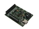
UMFT231XC is a USB to UART development module with battery charging support.
1
Introduction
UMFT231XC is a development module designed
primarily for evaluating the battery charging
feature of FTDI’s X-Chip range of USB-interface
bridging ICs. This module is suitable for charging
single cell lithium-ion batteries.
UMFT231XC utilises an FT231XS and a battery
charging IC. FT231XS is one of the devices from
FTDI’s range of USB interface bridging IC devices.
FT231X is a USB to UART interface with a battery
charger detection feature, which can allow
batteries to be charged with a higher current from
a dedicated charger port (without the FT231X
being enumerated).
The module includes a LTC4053EDD, which is a
lithium-ion battery charger with thermal
regulation. FTDI X-Chips are designed to operate
with battery charger chips, such as the
LTC4053EDD, to facilitate charging a battery of a
device via USB slave port, with either 1 Amp of
current from a dedicated charger port or with up to
500mA from a USB host without violating USB
compliance regulations. The X-Chip family are
designed to implement this feature without the
requirement of external MOSFET or controller chips
to regulate the current divider network of the
LTC4053 chip.
The on-chip MTP ROM of the FT231XS is
programmed by default to support this specific
battery charging application. The MTP ROM can be
reconfigured to allow for adjustments using
FT_Prog. FT_Prog is available for free download
from the FTDI website.
1.1
Features
The UMFT231XC is fitted with a FT231XS. For a
full list of the FT231X’s features please see the
FT231X datasheet which can be found at the FTDI
website.
In addition to the features listed in the FT231X
datasheet, the UMFT231XC has the following
features:
Configured with a LTC4053EDD lithium-ion
battery charger
3 way 3.5mm screw terminal for connecting a
battery to the module
Thermal regulation safety feature
10 pin 0.1” female header used for UART
signals, 12 pin 0.1” female header for Power
and control
Status LEDs
Mini USB-B connector
Power MOSFET for suspending power supplied
to an external circuit from USB bus when in
USB suspend mode
Applications include
Prototyping and evaluating battery charging of
a device via a USB port
USB to UART communications
Use of FTDI devices in life support and/or safety applications is entirely at the user’s risk, and the user agrees
to defend, indemnify and hold harmless FTDI from any and all damages, claims, suits or expense resulting
from such use.
�UMFT231XC Datasheet
Version 1.0
Document Reference No.: FT_000521
Clearance No.: FTDI#
273
Table of Contents
1
Introduction ................................................................................... 1
1.1
Features ....................................................................................................... 1
2
Driver Support ................................................................................ 3
3
Ordering Information ..................................................................... 3
4
UMFT231XC Signals and Configurations ......................................... 4
4.1
UMFT231XC Pin Out ...................................................................................... 4
4.2
CN3 Signal Descriptions ................................................................................ 4
4.3
CN4 Signal Descriptions ................................................................................ 5
4.4
CN2 Signal Descriptions ................................................................................ 5
4.5
Jumper Configurations .................................................................................. 6
4.6
LEDS.............................................................................................................. 6
5
Battery Charging using an X-Chip ................................................... 7
6
MTP ROM Configuration .................................................................. 9
7
Module Dimensions ...................................................................... 10
8
UMFT231XA Module Circuit Schematic .......................................... 11
9
Contact Information ..................................................................... 12
Appendix A - List of Figures and Tables ................................................................. 13
Appendix B – Revision History .............................................................................. 14
2
Copyright © 2012 Future Technology Devices International Limited
�UMFT231XC Datasheet
Version 1.0
Document Reference No.: FT_000521
Clearance No.: FTDI#
273
2 Driver Support
Royalty-Free VIRTUAL COM PORT
Drivers (VCP) for:
Royalty-Free D2XX Direct Drivers
(USB Drivers + DLL S/W Interface) for:
Windows 7 32,64-bit
Windows 7 32,64-bit
Windows Vista
Windows Vista
Windows XP 32,64-bit
Windows XP 32,64-bit
Windows XP Embedded
Windows XP Embedded
Windows CE.NET 4.2 , 5.0 and 6.0
Windows CE.NET 4.2, 5.0 and 6.0
MAC OS OS-X
MAC OS OS-X
Linux 3.0and greater
Linux 3.0 and greater
Android
Android
The drivers listed above are all available to download for free from www.ftdichip.com. Various 3rd Party
Drivers are also available for various other operating systems - visit www.ftdichip.com for details.
3 Ordering Information
Module Code
Utilised IC Code
Description
UMFT231XC-01
FT231XS
USB to UART evaluation module with battery charger support.
3
Copyright © 2012 Future Technology Devices International Limited
�UMFT231XC Datasheet
Version 1.0
Document Reference No.: FT_000521
Clearance No.: FTDI#
273
4 UMFT231XC Signals and Configurations
4.1 UMFT231XC Pin Out
Pin
CN3
CN4
1
TXD
VBUS
2
RXD
VBATT
3
RTS#
VBATT
4
CTS#
GND
5
DTR#
GND
6
DSR#
SWPWR
7
DCD#
PWREN#
8
RI#
SLEEP#
9
3V3OUT
CHRG#
10
GND
FAULT#
11
ACPR#
12
Table 4.1 – UMFT231XC Pin-Out
GND
4.2 CN3 Signal Descriptions
Pin No.
Name
Type
1
TXD
Output
Transmit asynchronous data output.
2
RXD
Input
Receiving asynchronous data input.
3
RTS#
Output
4
CTS#
Input
5
DTR#
Output
6
DSR#
Input
Data set ready control input / handshake signal.
7
DCD#
Input
Data carrier detect control input.
8
RI#
Input
Ring indicator control input. When remote wake up is enabled in the internal MTP
ROM taking RI# low >20ms can be used to resume the PC USB host controller
from suspend.
9
3V3OUT
Power
Output
Description
Request to send control output / handshake signal.
Clear to send control input / handshake signal.
Data terminal ready control output / handshake signal.
3.3V output with a current limit of 50mA from the on chip LDO regulator. This pin
is decoupled with a 100nF capacitor to ground on the PCB module. The prime
purpose of this pin is to provide the 3.3V supply that can be used internally. 3.3V
will always be present when power is supplied to VBUS.
10
GND
Ground
Module ground supply pins
Table 4.2 – CN3 Pin-Out Description
4
Copyright © 2012 Future Technology Devices International Limited
�UMFT231XC Datasheet
Version 1.0
Document Reference No.: FT_000521
Clearance No.: FTDI#
273
4.3 CN4 Signal Descriptions
Pin No.
Name
Type
Description
1
VBUS
Power
Output
5V power output USB port. For a low power USB bus powered design, up to
100mA can be sourced from the USB host/hub and applied to the USB bus. A
maximum of 500mA can be sourced from the USB host/hub and applied to the
USB bus in a high power USB designs. A current draw up to 1A can be sourced
from a dedicated charger and applied to the USB bus. VBUS is an input for the
USB connector CN1.
2
VBATT
Power
Output
Connection to the battery’s positive terminal and LTC4053EDD regulated power
output used for charging the battery.
3
VBATT
Power
Output
Connection to the battery’s positive terminal and LTC4053EDD regulated power
output used for charging the battery.
4
GND
Ground
Module ground supply pins
5
GND
Ground
Module ground supply pins
6
SWPWR
Power
Output
Switchable power sourced from VBUS, when utilised VBUS shorted to SWPWR
when the FT231X is enumerated.
7
PWREN#
Output
Output is low after the device has been configured by USB, then high during
USB suspend mode. This is the default configuration, reprogramming the MTP
ROM can change this setup.
8
SLEEP#
Output
Low during USB suspend mode. This is the default configuration,
reprogramming the MTP ROM can change this setup.
9
CHRG#
Output
Low when battery is being charged. This is the default configuration,
reprogramming the MTP ROM can change this setup.
10
FAULT#
Output
Low when VBATT or NCT is out of range. This is the default configuration,
reprogramming the MTP ROM can change this setup.
11
ACPR#
Output
Low when VBUS is out of voltage range required to charge the battery. This is
the default configuration, reprogramming the MTP ROM can change this setup.
12
GND
Ground Module ground supply pins
Table 4.3 – CN4 Pin-Out Description
4.4 CN2 Signal Descriptions
The CN2 connector is a screw terminal. This connector can be used to connect the wires of a battery the
UMFT231XC module.
Pin No.
Name
Type
Description
1
+
Power
Positive power connection to the battery. Power is output from this pin when
charging; power is input through this pin when powering a load from the battery.
2
NTC
Safety
Feature
Negative Temperature Coefficient, a safety feature used to monitor the batteries
temperature, suspends charging when temperature falls out of the temperature
range of 0°C – 50°C (with a 2°C hysteresis at both thresholds).
3
Ground
Ground connection for the negative supply of the battery.
Table 4.4 – CN4 Pin Out Description
5
Copyright © 2012 Future Technology Devices International Limited
�UMFT231XC Datasheet
Version 1.0
Document Reference No.: FT_000521
Clearance No.: FTDI#
273
4.5 Jumper Configurations
JP1 is used to reconfigure the power sourced by the switched power net controlled by the CBUS1 line
connected to a MOSFET.
Jumper
Shorted
Factory
No.
Pins
Settings
JP1
Pin1-2
Default
Setting
Description
Source switchable power from USB VBUS input. With a default configuration
SWPWR power is shutdown when the FT231X has not enumerated. This
function supports limiting the current flow through the USB bus while in
suspend to meet USB compliancy regulations.
JP1
Pin2-3
Source switchable power from battery.
Table 4.5 – Solder Links JP1 Pin Description
JP2 is used to adjust the UMFT231XC to facilitate for a battery with or without an NTC line. If a battery has an NTC
line, pin 2 of CN2 should be connected to the NTC pin of the battery charger, however if there is no LTC line available
the NTC pin of the battery charger should be tired to ground using this jumper.
Jumper
Shorted
Factory
No.
Pins
Settings
JP2
Pin1-2
-
Description
If the charged battery has an NTC line. Connect the line to CN2 pin 2 and
configure JP2 to this mode. NTC is a temperature sensing safety feature used
to prevent the battery overheating.
If there is no NTC line available, then configure JP2 to this jumper setting.
This setting shorts the UMFT231XC’s NCT line to ground. This indicates that
JP2
Pin2-3
NCT is not available, and allows the battery charger to function without this
function.
Table 4.6 – Solder Links JP2 Pin Description
Default
Setting
4.6 LEDS
The SWPWR LED illuminates when the SWPWR net is powered up. With the default MTP ROM
configuration power to SWPWR is switched on and off by PWREN# to the MOSFET Q1. Q1 will be on when
enumerated and off when not enumerated. SWPWR can be sourced from either VBUS or VBATT
depending on the setting of JP1.
The ACPR# LED illuminates when voltage supplied to VBUS is above the under-voltage lockout threshold
and at least 35mV above VBATT (which means the voltage supplied is suitable for charging).
The CHRG# LED illuminates when the battery is being charged.
The FAULT# LED illuminates when a fault is detected. These detected faults can be either NTC being out
of range and a timeout occurring under trickle charge conditions.
6
Copyright © 2012 Future Technology Devices International Limited
�UMFT231XC Datasheet
Version 1.0
Document Reference No.: FT_000521
Clearance No.: FTDI#
273
5 Battery Charging using an X-Chip
An illustration of an X-Chip being used for battery charging functions is shown in Figure 5.1. The PROG
pin of the LTC4053 holds a current detection function that maintains a voltage of 1.5V to this pin and is
used to detect the current flowing from VPROG (1.5V) at this pin through a resistor network to Ground. The
amount of current from VPROG through the resistor network to Ground is directly proportion the amount of
current permitted to flow from VBUS to the battery. The battery charging current is defined by ICHG =
(IPROG).1000, where ICHG is the current charging the battery, IPROG is 1.5V/RPROG and RPROG is the resistance
between VPROG and Ground.
It is important that there is no other current source to the PROG pin other than VPROG to prevent an offset
in the battery charging current. The FTDI FT231X uses open drain outputs with no internal pull-ups for
BCD# and PWREN# to support this requirement. The X-Chip will allow the same CBUS function to be
reused with more than one pin, so if BCD# or PWREN# are needed elsewhere in the circuit a second
assignment of the required function should be made to a second pin and this pin can be routed
elsewhere.
The SHDN# pin of the LTC4053 is an active low input and when a logic low is applied to SHDN# the
current supply to the battery is suspended.
VBUS
VBUS
VCC
VCC
BCD#
R14
1K5
PWREN#
R13
4K32
BAT
PROG
SLEEP#
SHDN#
R11
R12
2K2
16K5
FTDI X-Chip
GND
GND
LTC4053EDD
GND
Figure 5.1 – Simplified X-Chip - Battery Charger interface
The required configuration of the BCD# Options of the MTP ROM for this application are given in Table
5.1.
A list of all the different current limits of the UMFT231XC is given in Table 5.2. If the BCD Options of the
MTP ROM is configured as shown in Table 5.1, when connected to dedicated charger port BCD# will be
tied to ground, PWERN# will be floating and SLEEP will be driven high. The current values give in Table
5.2 can be altered by changing the values of R12, R13 or R14 of the UMFT231XC. The default values of
these resistors are given in Figure 5.1.
A description of the signals used to control the limit of the current to battery is given in Table 5.3.
BCD Options:
BCD# Options:
(1) Battery Charger Enable
Enable
Enables the use of BCD_Charger#
function, allows for BCD_Charger# to
be driven low when a dedicated charger
port is connected.
(2) Force Power Enable
Disable
Disables the option of forcing PWREN#
to be driven low when a dedicated
charger port is connected.
(2) Force Power Enable
(3) De-activate Sleep
Enable
Prevents SLEEP# pin from driving low
when a dedicated charger port is
connected.
(3) De-activate Sleep
(1) Battery Charger Enable
7
Copyright © 2012 Future Technology Devices International Limited
�UMFT231XC Datasheet
Version 1.0
Document Reference No.: FT_000521
Clearance No.: FTDI#
273
Table 5.1 – Configuration of the BCD Options for the UMFT231XC
BCD# Logic State
PWREN# Logic State
SLEEP# Logic State
Current Limits
X
X
0
0mA
Floating
Floating
1
70mA
Floating
0
1
400mA
0
Floating
1
1000mA
Table 5.2 – Truth Table for the Charging Current
Signal
Signal Description
Signal Function for this Application
Battery Charger Detected (Active Low)
BCD#
An open drain to ground function that shorts
to ground when a dedicated charger port is
detected.
Power Enable (Active Low)
PWREN#
An open drain to ground function that shorts
to ground when the X-Chip has enumerated.
When the embedded MTP ROM of the FT231X is
configured correctly, BCD# can be used to allow
the supply a current greater than 500mA to the
battery when a dedicated charged is connected to
the USB bus. This module will charge a battery
with up to 1A when connected to a dedicated
charger port. Details on the default MTP ROM
configuration (which is suitable for this application)
are given in Section 6.
PWREN# can be used to allow the supply a current
up to 500mA to the battery when the X-Chip is
enumerated or up to 100mA when the X-Chip is
not enumerated and not suspended. This module
charges a battery with a 400mA current limit when
in enumerated. When the chip is not enumerated,
not connected to a dedicated charger port and not
in sleep mode the battery is charged with a limit of
70mA. The “Force Power Enable” option should be
disabled to prevent driving the PWREN# signal low
and influencing the batteries current limit when
connected to a dedicated charger port. For other
application enabling this option can be a benefit.
Details on the default MTP ROM configuration
(which is suitable for this application) are given in
Section 6.
SLEEP# can stop the supply of current to the
battery when in USB suspend mode and otherwise
not interfere. For this application, the SLEEP#
function needs to be configured to be disabled (i.e.
driven high) when connected to a dedicated
charger port. This is done by enabling “De-activate
Sleep” option.
USB suspend (Active Low Output)
SLEEP#
An open drain with an internal pull-up to
VCCIO (3.3V for this module). Shorts to
Ground when in USB suspend mode.
Details on the default MTP ROM configuration
(which is suitable for this application) are given in
Section 6.
Charge Current Program pin.
PROG
SHDN#
The LTC4053 maintains a voltage of 1.5V to
this pin and measures the current flow
through the resistor network to ground. The
measured current flow is proportional to the
limit of the charging current allowed by this
chip.
This pin functions with the BCD# and PWREN#.
The combined resistance from PROG to ground of
the three resistors R13, R14 and R12 change with
the status of BCD# and PWREN#. When either of
these pins are logic Low, the pin becomes shorted
to ground. No additional current is applied to these
pins, thus no offset occurs for the PROG current
reading.
This line is used when in USB suspend mode, in
this mode current flow through the USB bus must
be less than 500uA. The SHDN# function limits the
charger current to less than 25uA when active.
Charger Shutdown (Active Low Input)
Shuts down charger current.
Table 5.3 – Battery Charging Supporting Functions Table
8
Copyright © 2012 Future Technology Devices International Limited
�UMFT231XC Datasheet
Version 1.0
Document Reference No.: FT_000521
Clearance No.: FTDI#
273
6 MTP ROM Configuration
Following a power-on reset or a USB reset the FT231X will scan its internal MTP ROM and read the USB
configuration descriptors stored there. The default values programmed into the internal MTP ROM in the
FT231XQ used on the UMFT231XC are shown in Table 6.1.
Parameter
Value
Notes
USB Vendor ID (VID)
0403h
FTDI default VID (hex)
USB Product UD (PID)
6015h
FTDI default PID (hex)
Serial Number Enabled?
Yes
Serial Number
See Note
A unique serial number is generated and programmed into the
MTP ROM during final test of the FT231XC module.
Pull down I/O Pins in USB
Suspend
Disabled
Enabling this option will make the device pull down on the
UART interface lines when the power is shut off (PWREN# is
high).
Manufacturer Name
FTDI
Product Description
UMFT231XC
Max Bus Power Current
500mA
Power Source
Bus Powered
Device Type
FT231X
USB Version
0200
Remote Wake Up
Enabled
Taking RI# low will wake up the USB host controller from
suspend.
High Current I/Os
Disabled
Enables the high drive level on the UART and CBUS I/O pins.
Load VCP Driver
Enabled
Makes the device load the CVP driver interface for the device.
CBUS0
BCD_Charger#
Default configuration of CBUS0 – Drives low when a dedicated
charger port is connected the USB bus. Otherwise a floating
output pin.
Returns USB 2.0 device description to the host. Note: The
device is a USB 2.0 Full Speed device (12Mb/s) as opposed to
a USB 2.0 High Speed device (480Mb/s).
BCD Options:
(1) Battery Charger Enable
Enable
Enables the use of BCD_Charger# function, allows for
BCD_Charger# to be driven low when a dedicated charger
port is connected.
(2) Force Power Enable
Disable
Disables the option of forcing PWREN# to be driven low when
a dedicated charger port is connected.
(3) De-activate Sleep
Enable
Prevents SLEEP# pin from driving low when a dedicated
charger port is connected.
CBUS1
PWREN#
Default configuration of CBUS1 – Power enable (used to
switch SWPWR).
CBUS2
SLEEP#
Default configuration of CBUS2 – Drives low when in USB
suspend mode. Configured to be disabled (ties high by
internal pull-up) when using a dedicated charger port.
PWREN#
Default configuration of CBUS3 – Power enable. Low after USB
enumeration, high when the FT231X is connected to a USB
host/hub and not enumerated. Configured to be disabled
(floating output) when a dedicated charger port is connected
to the device.
CBUS3
Invert UART
Disabled
Inverts the UART signals.
Table 6.1 – Default Internal MTP ROM Configuration
The internal MTP ROM in the FT231X can be programmed over USB using the utility program FT_PROG.
FT_PROG can be downloaded from the www.ftdichip.com. Users who do not have their own USB vendor
9
Copyright © 2012 Future Technology Devices International Limited
�UMFT231XC Datasheet
Version 1.0
Document Reference No.: FT_000521
Clearance No.: FTDI#
273
ID but who would like to use a unique Product ID in their design can apply to FTDI for a free block of
unique PIDs. Contact FTDI Support (support1@ftdichip.com) for this service, also see TN_100 and
TN_101.
7 Module Dimensions
Figure 7.1 – UMFT231XC Module Dimensions
All dimensions are given in millimetres.
The UMFT231XC module exclusively uses lead free components, and is fully compliant with European
Union directive 2002/95/EC.
10
Copyright © 2012 Future Technology Devices International Limited
�UMFT231XC Datasheet
Version 1.0
Document Reference No.: FT_000521
Clearance No.: FTDI#
273
8 UMFT231XA Module Circuit Schematic
Figure 8.1 – Module Circuit Schematic
11
Copyright © 2012 Future Technology Devices International Limited
�UMFT231XC Datasheet
Version 1.0
Document Reference No.: FT_000521
Clearance No.: FTDI#
273
9 Contact Information
Head Office – Glasgow, UK
Branch Office – Hillsboro, Oregon, USA
Future Technology Devices International Limited
Unit 1, 2 Seaward Place, Centurion Business Park
Glasgow G41 1HH
United Kingdom
Tel: +44 (0) 141 429 2777
Fax: +44 (0) 141 429 2758
Future Technology Devices International Limited (USA)
7235 NW Evergreen Parkway, Suite 600
Hillsboro, OR 97123-5803
USA
Tel: +1 (503) 547 0988
Fax: +1 (503) 547 0987
E-mail (Sales)
E-mail (Support)
E-mail (General Enquiries)
E-Mail (Sales)
E-Mail (Support)
E-Mail (General Enquiries)
sales1@ftdichip.com
support1@ftdichip.com
admin1@ftdichip.com
us.sales@ftdichip.com
us.support@ftdichip.com
us.admin@ftdichip.com
Branch Office – Taipei, Taiwan
Branch Office – Shanghai, China
Future Technology Devices International Limited (Taiwan)
2F, No. 516, Sec. 1, NeiHu Road
Taipei 114
Taiwan , R.O.C.
Tel: +886 (0) 2 8791 3570
Fax: +886 (0) 2 8791 3576
Future Technology Devices International Limited (China)
Room 408, 317 Xianxia Road,
Shanghai, 200051
China
Tel: +86 21 62351596
Fax: +86 21 62351595
E-mail (Sales)
E-mail (Support)
E-mail (General Enquiries)
E-mail (Sales)
E-mail (Support)
E-mail (General Enquiries)
tw.sales1@ftdichip.com
tw.support1@ftdichip.com
tw.admin1@ftdichip.com
cn.sales@ftdichip.com
cn.support@ftdichip.com
cn.admin@ftdichip.com
Web Site
http://ftdichip.com
Distributor and Sales Representatives
Please visit the Sales Network page of the FTDI Web site for the contact details of our distributor(s) and sales
representative(s) in your country.
System and equipment manufacturers and designers are responsible to ensure that their systems, and any Future Technology Devices International Ltd
(FTDI) devices incorporated in their systems, meet all applicable safety, regulatory and system-level performance requirements. All application-related
information in this document (including application descriptions, suggested FTDI devices and other materials) is provided for reference only. While FTDI
has taken care to assure it is accurate, this information is subject to customer confirmation, and FTDI disclaims all liability for system designs and for any
applications assistance provided by FTDI. Use of FTDI devices in life support and/or safety applications is entirely at the user’s risk, and the user agrees to
defend, indemnify and hold harmless FTDI from any and all damages, claims, suits or expense resulting from such use. This document is subject to change
without notice. No freedom to use patents or other intellectual property rights is implied by the publication of this document. Neither the whole nor any part
of the information contained in, or the product described in this document, may be adapted or reproduced in any material or electronic form without the prior
written consent of the copyright holder. Future Technology Devices International Ltd, Unit 1, 2 Seaward Place, Centurion Business Park, Glasgow G41
1HH, United Kingdom. Scotland Registered Company Number: SC136640
12
Copyright © 2012 Future Technology Devices International Limited
�UMFT231XC Datasheet
Version 1.0
Document Reference No.: FT_000521
Clearance No.: FTDI#
273
Appendix A - List of Figures and Tables
List of Figures
Figure 5.1 – Simplified X-Chip - Battery Charger interface ......................................................................... 7
Figure 7.1 – UMFT231XC Module Dimensions ........................................................................................... 10
Figure 8.1 – Module Circuit Schematic........................................................................................................ 11
List of Tables
Table 4.1 – UMFT231XC Pin-Out .................................................................................................................... 4
Table 4.2 – CN3 Pin-Out Description ............................................................................................................. 4
Table 4.3 – CN4 Pin-Out Description ............................................................................................................. 5
Table 4.4 – CN4 Pin Out Description ............................................................................................................. 5
Table 4.5 – Solder Links JP1 Pin Description ............................................................................................... 6
Table 4.6 – Solder Links JP2 Pin Description ............................................................................................... 6
Table 5.1 – Configuration of the BCD Options for the UMFT231XC ........................................................... 8
Table 5.2 – Truth Table for the Charging Current ........................................................................................ 8
Table 5.3 – Battery Charging Supporting Functions Table ......................................................................... 8
Table 6.1 – Default Internal MTP ROM Configuration .................................................................................. 9
13
Copyright © 2012 Future Technology Devices International Limited
�UMFT231XC Datasheet
Version 1.0
Document Reference No.: FT_000521
Clearance No.: FTDI#
273
Appendix B – Revision History
Document Title:
UMFT231XC
Document Reference No.:
FT_000521
Clearance No.:
FTDI# 273
Product Page:
http://www.ftdichip.com/FT-X.htm
Document Feedback:
Send Feedback
Version 1.0
Initial Datasheet Created
09/02/12
14
Copyright © 2012 Future Technology Devices International Limited
�


 工商网监
湘ICP备2023018690号
工商网监
湘ICP备2023018690号
