UMFT313EV Datasheet
Version 1.1
Document Reference No.: FT_000762
Clearance No.: FTDI# 321
Future Technology
Devices International
Ltd
UMFT313EV
Development Module
Datasheet
General Purpose USB2.0 Hi-Speed USB Host Controller
1 Introduction
The UMFT313EV is a development module for
FTDI’s FT313H, which is used to develop and
demonstrate the functionality of the USB2.0 HiSpeed Host Controller. This module can provide
three kinds of asynchronous bus interface to
connect with a microcontroller.
1.1 Features
The UMFT313EV utilises the FTDI FT313H QFN
package. All the features of the FT313H can be
accessed with the UMFT313EV. For a full list of the
FT313H’s features please see the FT313H datasheet.
In addition to the features listed in the FT313H
datasheet, the UMFT313EV has the following
features:
8-bit / 16-bit SRAM asynchronous bus interface
8-bit / 16-bit NOR Flash asynchronous bus
interface
Standard USB-A receptacle allows module to be
connected to USB devices
8-bit / 16-bit General Multiplex asynchronous
bus interface
Supports self-power
or power
microcontroller platform
In addition, FT313H also supports a battery
charger detection feature, which can allow
batteries to be charged with a higher current from
downstream
ports
with
three
kinds
of
configuration.
Provides configuration switch for module system
frequency selection and BCD mode configuration
Provides button for module hardware reset
On board 2x20 pins 2.54mm (0.1”) pitch female
headers allowing
easy
connection to
microcontroller platforms
Provides probe header for customer debugging
Standard downstream port (SDP)
Dedicated charging port (DCP)
Charging downstream port (CDP)
from
the
Neither the whole nor any part of the information contained in, or the product described in this manual, may be adapted or reproduced
in any material or electronic form without the prior written consent of the copyright holder. This product and its documentation are
supplied on an as-is basis and no warranty as to their suitability for any particular purpose is either made or implied. Future Technology
Devices International Ltd will not accept any claim for damages howsoever arising as a result of use or failure of this produ ct. Your
statutory rights are not affected. This product or any variant of it is not intended for use in any medical appliance, device or system in
which the failure of the product might reasonably be expected to result in personal injury. This document provides preliminar y
information that may be subject to change without notice. No freedom to use patents or other intellectual property rights is implied by
the publication of this document. Future Technology Devices International Ltd, Unit 1, 2 Seaward Place, Centurion Business Park,
Glasgow G41 1HH United Kingdom. Scotland Registered Company Number: SC136640
Copyright © Future Technology Devices International Limited
1
�UMFT313EV Datasheet
Version 1.1
Document Reference No.: FT_000762
Clearance No.: FTDI#
321
2 Ordering Information
Part No.
Description
UMFT313EV
FT313H Hi-Speed USB host controller development module.
Table 2-1 – Ordering information
Copyright © Future Technology Devices International Limited
2
�UMFT313EV Datasheet
Version 1.1
Document Reference No.: FT_000762
Clearance No.: FTDI#
321
Table of Contents
1
Introduction .................................................................... 1
1.1
Features .................................................................................... 1
2
Ordering Information ...................................................... 2
3
Hardware Description ..................................................... 4
3.1
UMFT313EV board profile .......................................................... 4
3.2
Physical Descriptions ................................................................ 5
3.2.1
PCB layout ................................................................................................ 5
3.2.2
Connectors ............................................................................................... 5
3.2.3
LEDs ...................................................................................................... 12
3.3
4
5
How to Quick Start .................................................................. 13
3.3.1
Establishment of hardware environment ..................................................... 13
3.3.2
Run Software .......................................................................................... 15
Board Circuit Schematics and BoMs............................... 16
4.1
UMFT313EV Schematic ............................................................ 16
4.2
Bill of Materials ....................................................................... 20
Contact Information ...................................................... 22
Appendix A – References ................................................... 23
Document References ..................................................................... 23
Acronyms and Abbreviations ........................................................... 23
Appendix B - List of Figures and Tables ............................. 24
List of Figures ................................................................................. 24
List of Tables ................................................................................... 24
Appendix C – Revision History ........................................... 25
Copyright © Future Technology Devices International Limited
3
�UMFT313EV Datasheet
Version 1.1
Document Reference No.: FT_000762
Clearance No.: FTDI#
321
3 Hardware Description
3.1 UMFT313EV board profile
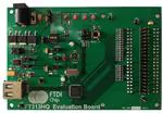
Figure 3.1 – UMFT313EV Board Profile
The UMFT313EV module is intended for use as a hardware platform to enable easy evaluation of FTDI’s
FT313H USB2.0 Hi-Speed host controller. This module is targeted at connecting with an external
microcontroller platform to control its parallel I/O bus interface.
The board requires a 5V DC supply with LEDs to indicate VCC(I/O) and VCC(3V3). A 12MHz oscillator
provides a clock to the FT313H. The reset button will perform a hardware reset and set the device to a
default mode.
If a microcontroller platform has installed the FT313H USB host software in initialization, the UMFT313EV
downstream port behaves as a general purpose USB2.0 Hi-Speed host controller, which is able to
support high speed / full speed / low speed USB devices and support all USB transfer types.
Copyright © Future Technology Devices International Limited
4
�UMFT313EV Datasheet
Version 1.1
Document Reference No.: FT_000762
Clearance No.: FTDI#
321
3.2 Physical Descriptions
3.2.1
PCB layout
The UMFT313EV module is 120mm x 80mm
approximately 1.6mm.
four-layer printed circuit board. Board thickness is
Figure 3.2 – UMFT313EV module top view
3.2.2
Connectors
Connectors and jumpers are described in the following sections.
Connector
Function
CN1
Standard-A USB host connector
CN2
Clock input, SMA connector; (Not populated)
CN3
+5V DC power connector
CN4
Prober connector, 2x20 pins male header; mounted on top
CN5
Bus interface connector, 2x20 pins female header; mounted on bottom
CN6
Power supply from platform connector, 2x20 pins female header; mounted on bottom
SW1
Reset push button
SW2
Chip operating mode configuration switch
SW3
DC power switch
Copyright © Future Technology Devices International Limited
5
�UMFT313EV Datasheet
Version 1.1
Document Reference No.: FT_000762
Connector
321
Function
JP1
VCC(1V2) power supply jumper
JP2
VCC(3V3) power supply jumper
JP3
VCC(I/O) power supply jumper
JP4
OC_N signal configuration jumper
JP5
PSW_N signal configuration jumper
JP6
Chip entry test mode jumper
JP7
ALE signal configuration jumper
JP8
CLE signal configuration jumper
JP9
+5V power supply jumper
JP10
Clearance No.: FTDI#
VCC(I/O) power supply resource jumper
Table 3-1 – Connectors and Jumpers
CN1- USB port
Standard USB-A receptacle for USB device connection.
CN2- Clock input connector
This is an option for the FT313H clock input. By default, this component is not populated on the PCB.
To use CLKIN for a clock input, remove R9 0 ohm resistor on the board and select the correct
frequency configuration on SW2.
CN3- DC power connector
Used for external power supply of +5V / 3A from DC power supply.
As the FT313H supports high current battery charging in CDP and DCP mode, it is recommended to
use an external power supply for charging. Note, the SW3 power switch controls external power (on
or off).
By default, the UMFT313EV module uses the +5V voltage power supply from the host microcontroller
platform.
CN4- Probe connector
For customer debug when developing code for the UMFT313EV module on a specific platform. The
table below lists the pinout description.
Pin No.
Name
Type
Description
Power supply detector
1
PS_D
O
1 -- Power supply from micro controller
platform
0 -- Power supply from external wall
adapter
2
RD#
I
Read enable, active low
3
Reserved
-
-
4
CS#
I
Chip select, active low
5
INTERRUPT
O
Interrupt output, default active low
Copyright © Future Technology Devices International Limited
6
�UMFT313EV Datasheet
Version 1.1
Document Reference No.: FT_000762
Pin No.
Name
Type
Clearance No.: FTDI#
321
Description
Polarity control by register
6
WR#
I
Write enable, active low
7
DMA_DACK
I
8
DMA_DREQ
O
9
DATA0
I/O
Address and data bus bit 0
10
DATA1
I/O
Address and data bus bit 1
11
Reserved
-
-
12
GND
P
Ground
13
DATA2
I/O
Address and data bus bit 2
14
DATA3
I/O
Address and data bus bit 3
15
DATA4
I/O
Address and data bus bit 4
16
DATA5
I/O
Address and data bus bit 5
17
DATA6
I/O
Address and data bus bit 6
18
DATA7
I/O
Address and data bus bit 7
19
RST#
I
Asynchronous reset, active low
20
ALE_T
I
Address latch enable
21
Reserved
-
-
22
CLE_T
I
Command latch enable
23
DATA8
I/O
Address and data bus bit 8
24
DATA9
I/O
Address and data bus bit 9
25
DATA10
I/O
Address and data bus bit 10
26
DATA11
I/O
Address and data bus bit 11
27
DATA12
I/O
Address and data bus bit 12
28
DATA13
I/O
Address and data bus bit 13
29
Reserved
-
-
30
GND
P
Ground
31
DATA14
I/O
Address and data bus bit 14
32
DATA15
I/O
Address and data bus bit 15
33
ADDR0
I
Address bus bit 0
34
ADDR1
I
Address bus bit 1
35
ADDR2
I
Address bus bit 2
36
ADDR3
I
Address bus bit 3
37
ADDR4
I
Address bus bit 4
38
ADDR5
I
Address bus bit 5
39
ADDR6
I
Address bus bit 6
DMA acknowledge, default active low
Polarity control by register
DMA request, default active low
Polarity control by register
Copyright © Future Technology Devices International Limited
7
�UMFT313EV Datasheet
Version 1.1
Document Reference No.: FT_000762
Pin No.
Name
Type
40
ADDR7
I
Clearance No.: FTDI#
321
Description
Address bus bit 7
Table 3-2 – CN4 Probe Pinout Description
CN5- Bus interface connector
This header connects to the external development platform which can access the FT313H chip by PIO
mode or DMA mode. Also, provides +5V power supply to UMFT313EV module. The table below lists
the pinout description.
Pin No.
Name
Type
Description
Power supply detector
1
PS_D
O
1 -- Power supply from micro controller
platform
0 -- Power supply from external wall
adapter
2
RD#
I
Read enable, active low
3
Reserved
-
-
4
CS#
I
Chip select, active low
5
INTERRUPT
O
6
WR#
I
7
DMA_DACK
I
8
DMA_DREQ
O
9
DATA0
I/O
Address and data bus bit 0
10
DATA1
I/O
Address and data bus bit 1
11
5V_FPGA
P
+5V power supply
12
GND
P
Ground
13
DATA2
I/O
Address and data bus bit 2
14
DATA3
I/O
Address and data bus bit 3
15
DATA4
I/O
Address and data bus bit 4
16
DATA5
I/O
Address and data bus bit 5
17
DATA6
I/O
Address and data bus bit 6
18
DATA7
I/O
Address and data bus bit 7
19
RST#
I
Asynchronous reset, active low
20
ALE_T
I
Address latch enable
21
Reserved
-
-
22
CLE_T
I
Command latch enable
Interrupt output, default active low
Polarity control by register
Write enable, active low
DMA acknowledge, default active low
Polarity control by register
DMA request, default active low
Polarity control by register
Copyright © Future Technology Devices International Limited
8
�UMFT313EV Datasheet
Version 1.1
Document Reference No.: FT_000762
Clearance No.: FTDI#
Pin No.
Name
Type
23
DATA8
I/O
Address and data bus bit 8
24
DATA9
I/O
Address and data bus bit 9
25
DATA10
I/O
Address and data bus bit 10
26
DATA11
I/O
Address and data bus bit 11
27
DATA12
I/O
Address and data bus bit 12
28
DATA13
I/O
Address and data bus bit 13
29
3.3V_FPGA
P
+3.3V power supply
30
GND
P
Ground
31
DATA14
I/O
Address and data bus bit 14
32
DATA15
I/O
Address and data bus bit 15
33
ADDR0
I
Address bus bit 0
34
ADDR1
I
Address bus bit 1
35
ADDR2
I
Address bus bit 2
36
ADDR3
I
Address bus bit 3
37
ADDR4
I
Address bus bit 4
38
ADDR5
I
Address bus bit 5
39
ADDR6
I
Address bus bit 6
40
ADDR7
I
Address bus bit 7
321
Description
Table 3-3 – CN5 Bus Interface Pinout Description
CN6- Platform Power Connector
This header provides power and ground to UMFT313EV module. The table below lists the pinout
description.
Pin No.
Name
Type
Description
1
Reserved
-
-
2
Reserved
-
-
3
Reserved
-
-
4
Reserved
-
-
5
Reserved
-
-
6
Reserved
-
-
7
Reserved
-
-
8
Reserved
-
-
9
Reserved
-
-
10
Reserved
-
-
11
5V_FPGA
P
+5V power supply
Copyright © Future Technology Devices International Limited
9
�UMFT313EV Datasheet
Version 1.1
Document Reference No.: FT_000762
Pin No.
Name
Type
12
GND
P
Ground
13
Reserved
-
-
14
Reserved
-
-
15
Reserved
-
-
16
Reserved
-
-
17
Reserved
-
-
18
Reserved
-
-
19
Reserved
-
-
20
Reserved
-
-
21
Reserved
-
-
22
Reserved
-
-
23
Reserved
-
-
24
Reserved
-
-
25
Reserved
-
-
26
Reserved
-
-
27
Reserved
-
-
28
Reserved
-
-
29
3.3V_FPGA
P
+3.3V power supply
30
GND
P
Ground
31
Reserved
-
-
32
Reserved
-
-
33
Reserved
-
-
34
Reserved
-
-
35
Reserved
-
-
36
Reserved
-
-
37
Reserved
-
-
38
Reserved
-
-
39
Reserved
-
-
40
Reserved
-
-
Clearance No.: FTDI#
321
Description
Table 3-4 – CN6 power and ground pinout description
SW1- Reset push button
Hardware reset button. Active low.
SW2- Chip configuration switch
This switch is provided for BCD mode configuration and system clock frequency selection.
Oscillator is the on-board default, and USB port is default setup to SDP.
12MHz
(SW2 ON position = ‘0’; OFF position = ‘1’)
Copyright © Future Technology Devices International Limited
10
�UMFT313EV Datasheet
Version 1.1
Document Reference No.: FT_000762
SW2
BCD MODE
Standard
Downstream Port
Dedicated Charging
Port
(SDP) –Default
setting
(DCP)
Clearance No.: FTDI#
321
Charging
Downstream
Port
(CDP)
SW2.1
CPE1
0
0
1
SW2.2
CPE0
0
1
1
Table 3-5 – BCD Mode Configuration
(SW2 ON position =’0’; OFF position = ‘1’)
SW2
12MHz
CLK
FREQUENCE
(Default setting)
SW2.3
FREQSEL2
SW2.4
FREQSEL1
19.2MHz
24MHz
0
0
1
0
1
0
Table 3-6 – System clock frequency selection
SW3- DC power switch
The external power supply switch. Default is off.
JP1/JP2/JP3- power supply jumper
JP1 – VCC(1V2) power supply jumper, default is short.
Chip core voltage output VOUT(1V2) connects to VCC(1V2) input with this jumper. User can
utilize this header to measure power consumption for core power supply.
JP2 – VCC(3V3) power supply jumper, default is short.
Utilize this header to measure power consumption for VCC(3V3) power supply.
JP3 – VCC(I/O) power supply jumper, default is short.
Utilize this header to measure power consumption for VCC(I/O) power supply.
JP4/JP5- OC_N/PSW_N signals jumper
JP4 – +5V tolerant support, for debug.
By default, OC_N pin (Active low) connects to VCC(3V3) through a 10k ohm resistor.
Connect pin 1 and pin 2. OC_N pin connected to +5V.
Connect pin 2 and pin 3. OC_N pin connected to VCC(3V3).
JP5 – +5V tolerant support, for debug.
By default, PSW_N pin (Active low) connects to VCC(3V3) through a 10k ohm resistor.
Connect pin 1 and pin 2. PSW_N pin connected to +5V.
Connect pin 2 and pin 3. PSW_N pin connected to VCC(3V3).
JP6- Test mode jumper
This jumper is only for factory test.
The header should be left open for normal operation.
Copyright © Future Technology Devices International Limited
11
�UMFT313EV Datasheet
Version 1.1
Document Reference No.: FT_000762
Clearance No.: FTDI#
321
JP7/JP8- ALE/CLE signals jumper
ALE and CLE are provided to select the FT313H bus interface type, please see jumper schematic in
Figure 4.2.
JUMPER
SIGNAL
SRAM
NOR
General
Multiplex
JP7
ALE
1 (JP7 1-2 short)
1 (JP7 1-2 short)
0 (JP7 2-3 short)
JP8
CLE
1 (JP8 1-2 short)
0 (JP8 2-3 short)
0 (JP8 1-2 short)
Table 3-7 – Bus Interface Configuration
JP9- +5V power supply jumper
Connect 5V_USB to 5V_EXT, if using an external power supply through CN3 connector.
Connect 5V_USB to 5V_FPGA, by default use microcontroller platform power supply through CN5 and
CN6 connectors.
JP10- VCC(I/O) power resource jumper
The FT313H chip supports bus interface I/O voltage from 1.62V to 3.63V. There are three selectable
supplies on board which can provide the VCC(I/O) voltage. By default, +3.3V voltage is connected to
VCC(I/O).
Connect VCC(I/O) to +3.3V, bus interface I/O signals support +3.3V tolerance.
Connect VCC(I/O) to +2.5V, bus interface I/O signals support +2.5V tolerance.
Connect VCC(I/O) to +1.8V, bus interface I/O signals support +1.8V tolerance.
3.2.3
LEDs
The UMFT313EV module has four LEDs that are located on the top side of the board.
LED
Use
Color
LED1
VBUS indicator
Red
LED2
+5V power indicator
Green
LED3
VCC(I/O) power indicator
Green
LED4
VCC(3V3) power indicator
Table 3-8 – LEDs
Green
Copyright © Future Technology Devices International Limited
12
�UMFT313EV Datasheet
Version 1.1
Document Reference No.: FT_000762
Clearance No.: FTDI#
321
3.3 How to Quick Start
This section explains how the UMFT313EV module may be setup for code development. For more
information, refer to the FT313H application notes.
3.3.1
Establishment of hardware environment
Figure 3.3 – PCI Express FPGA Development Setup
Note: This setup assumes the UMFT313EV is to be connected to a desktop PC for software development.
Users with a standard processor board support package would not necessarily need the PCI bridge and
may connect direct to the target processor.
1). X86-based PC that has PCI Express slot (minimum 4x connector) in motherboard
Installed Linux OS with CentOS 6.3.
http://mirror.nus.edu.sg/centos/6.3/isos/i386/
Rebuild Kernel version 3.0.4 with download from kernel.org.
http://www.kernel.org/pub/linux/kernel/v3.0/linux-3.0.4.tar.gz
2). PCI Express extender cable
The PCI Express provides a high-speed, high-performance, point-to-point, differential signaling link for
interconnecting devices. Data is transmitted form a device on one set of signals, and received on another
set of signals.
Copyright © Future Technology Devices International Limited
13
�UMFT313EV Datasheet
Version 1.1
Document Reference No.: FT_000762
Clearance No.: FTDI#
321
This PCI Express extender cable interconnect consists of either an x1, x2, x4 point-to-point link.
Can be purchased from the Samtec website.
https://www.samtec.com/productinformation/technicalspecifications/overview.aspx?series=pciec
3). Altera Cyclone IV GX FPGA development kit
The Altera Cyclone IV GX FPGA development kit is a PCI-SIG compliant board which supports PCI Express
Gen x1, x2, and x4 endpoint designs with using Cyclone IV GX PCI Express hard intellectual property(IP).
Download FPGA image .flash file into NAND flash memory on board. This image will be provided by FTDI.
Power on the FPGA platform after all the boards are connected, then power on PC with power button. The
PCI Express system will do a hardware reset for UMFT313EV module.
Can be purchased from the Altera website.
http://www.altera.com/products/devkits/altera/kit-cyclone-iv-gx.html
4). Terasic GPIO-HSMC card
This board is designed to fan out the High Speed Mezzanine connector (HSMC) I/Os to three 40-pin
expansion prototype connector. This board connects the Altera Cyclone IV GX FPGA development kit
HSMC-A header to UMFT313EV module CN5 and CN6 headers.
Please note to short JP3 jumper on Altera FPGA development kit to provide +2.5V voltage on HSMC-A
header.
Can be purchased from the Terasic website.
GPIO-HSMC Card:
http://www.terasic.com.tw/cgi-bin/page/archive.pl?Language=English&CategoryNo=67&No=218
GPIO-HSTC Card: (New model instead of GPIO-HSMC Card)
http://www.terasic.com.tw/cgi-bin/page/archive.pl?Language=English&CategoryNo=67&No=322
5). UMFT313EV development module
Please note to select JP9 jumper 5V_USB connect to 5V_FPGA, and select JP10 jumper VCC(I/O) to
connect to +2.5V.
6). USB device
Any USB2.0 Hi-Speed , full-speed, low-speed devices or hubs.
Copyright © Future Technology Devices International Limited
14
�UMFT313EV Datasheet
Version 1.1
Document Reference No.: FT_000762
3.3.2
Clearance No.: FTDI#
321
Run Software
The UMFT313EV module USB host controller driver software stack will be provided by FTDI Chip. For more
Information, refer to the FT313H software programming guide.
Function driver 1
Function driver 2
Function driver n
USB Driver
FT313H Host Controller Driver
System Bus
FT313H Hardware
Figure 3.4 – USB host controller software architecture
1). Login PC, go to FT313H-hcd project folder.
2). Install FT313H host controller device driver in system by command:
> make
> insmod ft313-hcd.ko
3). Insert USB2.0 high speed thumb drive, and see the mass storage device on window, and then doubleclick the icon to access the memory.
Copyright © Future Technology Devices International Limited
15
�UMFT313EV Datasheet
Version 1.1
Document Reference No.: FT_000762
Clearance No.: FTDI#
321
4 Board Circuit Schematics and BoMs
4.1 UMFT313EV Schematic
Figure 4.1 – FT313H Chip
Copyright © Future Technology Devices International Limited
16
�UMFT313EV Datasheet
Version 1.1
Document Reference No.: FT_000762
Clearance No.: FTDI#
321
Figure 4.2 – Configuration
Copyright © Future Technology Devices International Limited
17
�UMFT313EV Datasheet
Version 1.1
Document Reference No.: FT_000762
Clearance No.: FTDI#
321
Figure 4.3 – Power
Copyright © Future Technology Devices International Limited
18
�UMFT313EV Datasheet
Version 1.1
Document Reference No.: FT_000762
Clearance No.: FTDI#
321
Figure 4.4 – Connector
Copyright © Future Technology Devices International Limited
19
�UMFT313EV Datasheet
Version 1.1
Document Reference No.: FT_000762
Clearance No.: FTDI#
321
4.2 Bill of Materials
#
Comment
Designator
Footprint
Description
1
0.1uF
C1, C4, C5, C6, C7,
C9, C10, C11, C12,
C13, C14, C21, C22,
C26, C29, C33
CAPC1608-0603
Capacitor bipolar
2
150uF/10V
C2
CAPM-C-6032-28
CAP TANT 150UF 10V 10% 2312
3
4.7uF
C3, C18, C19, C23,
C30
CAPM-A-3216-18
Polarized Capacitor
4
10uF
C8, C25, C28, C32
CAPM-B-3528-21
CAP TANT 10UF 25V 10% 1411
5
1nF
C15
CAPC1608-0603
Capacitor bipolar
6
27pF
C16, C17
CAPC1608-0603
Capacitor bipolar
7
47uF/10V
C20
CAPM-B-3528-21
Polarized Capacitor
8
1uF
C24, C27, C31
CAPM-A-3216-18
CAP TANT 10UF 25V 10% 1411
9
USB Type A
Receptacle
CN1
CN_USB-SKT A
USB connector
10
2.1mm Power
Jack
CN3
CN_2.1mm_POW
ER_SOCKET
Low Voltage Power Supply
Connector
11
LA Probe,
Male Header,
40-Pin, Place
to top
CN4
CN_HDR2X20
CONN HEADER VERT DUAL
40POS GOLD
12
Terasic JP2
Female
Header, 40Pin, Place to
bottom
CN5
CN_HDR2X20
Header, 40-Pin, Dual row
13
Terasic JP1
Female
Header, 40Pin, Place to
bottom
CN6
CN_HDR2X20
Header, 40-Pin, Dual row
14
600R/2A
FB1
IND_C2012-0805
Chip Ferrite Bead 0805
15
Header1 x2
JP1, JP2, JP3, JP6
SIP-2
2 contact jumper
16
Header1 x3
JP4, JP5, JP7, JP8,
JP9
SIP-3
3 contact jumper
17
Header2 x3
JP10
CN_HDR2X3
2 contact jumper
18
Red
LED1
LEDC2012-0805
Typical LED diode
19
Green
LED2, LED3, LED4
LEDC2012-0805
Typical LED diode
20
470R
R1
RESC1608-0603
Resistor
21
0R
R2, R3, R9, R23,
R25, R26, R27, R28,
R29, R30, R31, R32,
R33, R34, R35, R36,
R37, R38, R39, R40,
R41, R42, R44, R45,
R47, R48, R49, R50,
RESC1608-0603
Resistor
Copyright © Future Technology Devices International Limited
20
�UMFT313EV Datasheet
Version 1.1
Document Reference No.: FT_000762
#
Comment
Designator
Footprint
Description
Clearance No.: FTDI#
321
R51, R52, R53, R54,
R55, R56, R57, R58,
R59, R60
22
10K
R4, R5, R7, R12,
R13, R14, R15, R16,
R17, R18, R43, R46
RESC1608-0603
Resistor
23
12K +/-1%
R6
RESC1608-0603
Resistor
24
100R
R10
RESC1608-0603
Resistor
25
1K
R11
RESC1608-0603
Resistor
26
360R
R21, R24
RESC1608-0603
Resistor
27
200R
R22
RESC1608-0603
Resistor
28
EVQPAC04
SW1
SW_PushButton
Push button momentary switch;
4.3 - 5.0mm height
29
Switch DIP
SW2
SW_DIP_TDA04H
0SB1
SWITCH DIP 4POS HALF PITCH
SMD
30
Switch slide
SW3
SW_500ASSP1M2
SWITCH SLIDE MINI SPDT PC
MNT, LF
31
Red
TP1, TP2, TP10,
TP11, TP12, TP13
TEST_PIN_PTH_C
OMPACT
Test pin
32
White
TP3, TP4
TEST_PIN_PTH_C
OMPACT
Test pin
33
Black
TP5, TP6, TP7, TP8,
TP9
TEST_PIN_PTH_C
OMPACT
TEST POINT PC COMPACT
.063"D BLK
34
FT313HQ
U1
QFN50P900X90064N
HS USB Host Controller, Single
USB Port, USB2.0 EHCI
Compatible
35
TPS2024D
U2
SO-8N
Power distribution switches
36
LD1086DT33T
R
U3
TO252P990X2383N
1.5A Low Dropout Positive
Voltage Regulator
37
LD1086DT25T
R
U4
TO252P990X2383N
1.5A Low Dropout Positive
Voltage Regulator
38
LD1086DT18T
R
U5
TO252P990X2383N
1.5A Low Dropout Positive
Voltage Regulator
39
NC7SZ05M5X
U6
SOT23-5AL
IC INVERT SGL OPEN DRAIN
SOT23-5
40
Shunt Jumper
2.54mm
XL1, XL2, XL3, XL4,
XL5, XL6, XL7, XL8,
XL9, XL10
41
12MHz
Y1
-
2.54mm Shorting Jumper
CRYSTAL_HC49_
Crystal Oscillator
3Pin
Table 4-1 – Bill of materials
Copyright © Future Technology Devices International Limited
21
�UMFT313EV Datasheet
Version 1.1
Document Reference No.: FT_000762
Clearance No.: FTDI#
321
5 Contact Information
Head Office – Glasgow, UK
Branch Office – Tigard, Oregon, USA
Unit 1, 2 Seaward Place, Centurion Business Park
Glasgow G41 1HH
United Kingdom
Tel: +44 (0) 141 429 2777
Fax: +44 (0) 141 429 2758
7130 SW Fir Loop
Tigard, OR 97223
USA
Tel: +1 (503) 547 0988
Fax: +1 (503) 547 0987
E-mail (Sales)
E-mail (Support)
E-mail (General Enquiries)
E-Mail (Sales)
E-Mail (Support)
E-Mail (General Enquiries)
sales1@ftdichip.com
support1@ftdichip.com
admin1@ftdichip.com
us.sales@ftdichip.com
us.support@ftdichip.com
us.admin@ftdichip.com
Branch Office – Taipei, Taiwan
Branch Office – Shanghai, China
2F, No. 516, Sec. 1, NeiHu Road
Taipei 114
Taiwan , R.O.C.
Tel: +886 (0) 2 8797 1330
Fax: +886 (0) 2 8751 9737
Room 1103, No. 666 West Huaihai Road,
Changning District, Shanghai, 200052
China
Tel: +86 (0)21 6235 1596
Fax: +86 (0)21 6235 1595
E-mail (Sales)
E-mail (Support)
E-mail (General Enquiries)
E-mail (Sales)
E-mail (Support)
E-mail (General Enquiries)
tw.sales1@ftdichip.com
tw.support1@ftdichip.com
tw.admin1@ftdichip.com
cn.sales@ftdichip.com
cn.support@ftdichip.com
cn.admin@ftdichip.com
Web Site
http://ftdichip.com
Distributor and Sales Representatives
Please visit the Sales Network page of the FTDI Web site for the contact details of our distributor(s) and sales
representative(s) in your country.
System and equipment manufacturers and designers are responsible to ensure that their systems, and any Future Technology Devices
International Ltd (FTDI) devices incorporated in their systems, meet all applicable safety, regulatory and system-level performance
requirements. All application-related information in this document (including application descriptions, suggested FTDI devices and other
materials) is provided for reference only. While FTDI has taken care to assure it is accurate, this information is subject to customer
confirmation, and FTDI disclaims all liability for system designs and for any applications assistance provided by FTDI. Use of FTDI
devices in life support and/or safety applications is entirely at the user’s risk, and the user agrees to defend, indemnify and hold
harmless FTDI from any and all damages, claims, suits or expense resulting from such use. This document is subject to change without
notice. No freedom to use patents or other intellectual property rights is implied by the publication of this document. Neither the whole
nor any part of the information contained in, or the product described in this document, may be adapted or reproduced in any material
or electronic form without the prior written consent of the copyright holder. Future Technology Devices International Ltd, Unit 1, 2
Seaward Place, Centurion Business Park, Glasgow G41 1HH, United Kingdom. Scotland Registered Company Number: SC136640
Copyright © Future Technology Devices International Limited
22
�UMFT313EV Datasheet
Version 1.1
Document Reference No.: FT_000762
Clearance No.: FTDI# 321
Appendix A – References
Document References
FT313H IC Datasheet
FT313H Software Programming Guide
USB_2.0 - http://www.usb.org/developers/docs/usb20_docs/
EHCI Spec - Enhanced Host Controller Interface Specification for Universal Serial Bus Revision 1.0
PCI Express Spec - PCI Express Base Specification Revision 3.0
Altera Cyclone IV FPGA - Altera Cyclone IV GX FPGA Development Kit User Guide
Acronyms and Abbreviations
Term
Description
BCD
Battery Charger Detect
CPE0
Charging Port Emulation 0
CPE1
Charging Port Emulation 1
CDP
Charging Downstream Port
DCP
Dedicated Charging Port
HSMC
High Speed Mezzanine Connector
HSTC
High Speed Terasic Connector
LED
Light Emitting Diode
OS
Operating System
PCI
Peripheral Component Interconnect
QFN
Quad Flat No Lead Package
SDP
Standard Downstream Port
USB
Universal Serial Bus
Copyright © Future Technology Devices International Limited
23
�UMFT313EV Datasheet
Version 1.1
Document Reference No.: FT_000762
Clearance No.: FTDI# 321
Appendix B - List of Figures and Tables
List of Figures
Figure 3.1 – UMFT313EV Board Profile ............................................................................................. 4
Figure 3.2 – UMFT313EV module top view ....................................................................................... 5
Figure 3.3 – PCI Express FPGA Development Setup ......................................................................... 13
Figure 3.4 – USB host controller software architecture .................................................................... 15
Figure 4.1 – FT313H Chip ............................................................................................................ 16
Figure 4.2 – Configuration ........................................................................................................... 17
Figure 4.3 – Power ...................................................................................................................... 18
Figure 4.4 – Connector ................................................................................................................ 19
List of Tables
Table 2-1 – Ordering information .................................................................................................... 2
Table 3-1 – Connectors and Jumpers............................................................................................... 6
Table 3-2 – CN4 Probe Pinout Description ........................................................................................ 8
Table 3-3 – CN5 Bus Interface Pinout Description ............................................................................. 9
Table 3-4 – CN6 power and ground pinout description ..................................................................... 10
Table 3-5 – BCD Mode Configuration ............................................................................................. 11
Table 3-6 – System clock frequency selection................................................................................. 11
Table 3-7 – Bus Interface Configuration......................................................................................... 12
Table 3-8 – LEDs ........................................................................................................................ 12
Table 4-1 – Bill of materials ......................................................................................................... 21
Copyright © Future Technology Devices International Limited
24
�UMFT313EV Datasheet
Version 1.1
Document Reference No.: FT_000762
Clearance No.: FTDI# 321
Appendix C – Revision History
Document Title:
UMFT313EV Datasheet
Document Reference No.:
FT_000762
Clearance No.:
FTDI# 321
Product Page:
http://www.ftdichip.com/Products/Modules.htm
Document Feedback:
Send Feedback
Revision
Changes
Date
Version 1.0
Initial Release
2012-10-31
Version 1.1
Corrected Table 3-7 Jumper Settings
2018-06-26
Copyright © Future Technology Devices International Limited
25
�


 工商网监
湘ICP备2023018690号
工商网监
湘ICP备2023018690号
