Genesys Logic, Inc.
GL823K
USB 2.0 SD/MSPRO Card Reader
Controller
Datasheet
Revision 1.05
May 24, 2016
�GL823K Datasheet
Copyright
Copyright © 2016 Genesys Logic, Inc. All rights reserved. No part of the materials shall be reproduced in any
form or by any means without prior written consent of Genesys Logic, Inc.
Ownership and Title
Genesys Logic, Inc. owns and retains of its right, title and interest in and to all materials provided herein.
Genesys Logic, Inc. reserves all rights, including, but not limited to, all patent rights, trademarks, copyrights and
any other propriety rights. No license is granted hereunder.
Disclaimer
All Materials are provided “as is”. Genesys Logic, Inc. makes no warranties, express, implied or otherwise,
regarding their accuracy, merchantability, fitness for any particular purpose, and non-infringement of intellectual
property. In no event shall Genesys Logic, Inc. be liable for any damages, including, without limitation, any
direct, indirect, consequential, or incidental damages. The materials may contain errors or omissions. Genesys
Logic, Inc. may make changes to the materials or to the products described herein at anytime without notice.
Genesys Logic, Inc.
12F., No. 205, Sec. 3, Beixin Rd., Xindian Dist. 231,
New Taipei City, Taiwan
Tel : (886-2) 8913-1888
Fax : (886-2) 6629-6168
http ://www.genesyslogic.com
© 2016 Genesys Logic, Inc. - All rights reserved.
GLI Confidential
Page 2
�GL823K Datasheet
Revision History
Revision
Date
Description
1.00
06/13/2014
First formal release
1.01
06/18/2014
Add ordering information in Ch.7, p16
1.02
07/02/2014
Release for SSOP16 (150mil) package
1.03
12/17/2014
Modify Figure 3.1, p8
Add Ch5.3 DC Characteristics, p12
1.04
11/11/2015
Update Figure 6.1 – SSOP 16 Pin Package (150 mil), p.14
1.05
05/24/2016
Update CH2 Features
© 2016 Genesys Logic, Inc. - All rights reserved.
GLI Confidential
Page 3
�GL823K Datasheet
Table of Contents
CHAPTER 1 GENERAL DESCRIPTION .......................................................................... 6
CHAPTER 2 FEATURES...................................................................................................... 7
CHAPTER 3 PIN ASSIGMENT ........................................................................................... 8
3.1 SSOP16 Pinout .......................................................................................................... 8
3.2 Pin Description .......................................................................................................... 9
CHAPTER 4 BLOCK DIAGRAM ..................................................................................... 10
4.1 OCCS USB PHY ..................................................................................................... 10
4.2 SIE ............................................................................................................................ 10
4.3 EPFIFO .................................................................................................................... 10
4.4 MCU ......................................................................................................................... 10
4.5 MHE ......................................................................................................................... 11
4.6 Regulator ................................................................................................................. 11
4.7 PMOS ....................................................................................................................... 11
CHAPTER 5 ELECTRICAL CHARACTERISTICS ...................................................... 12
5.1 Temperature Conditions ......................................................................................... 12
5.2 Operating Conditions ............................................................................................. 12
5.3 DC Characteristics .................................................................................................. 12
5.4 Memory Card Clock Frequency ............................................................................ 12
CHAPTER 6 PACKAGE DIMENSION ............................................................................ 14
CHAPTER 7 ORDERING INFORMATION .................................................................... 15
© 2016 Genesys Logic, Inc. - All rights reserved.
GLI Confidential
Page 4
�GL823K Datasheet
List of Figures
Figure 3.1 – SSOP 16 Pinout Diagram ................................................................................... 8
Figure 6.1 – SSOP 16 Pin Package (150 mil) ........................................................................ 14
List of Tables
Table 3.1 – Pin Description ...................................................................................................... 9
Table 4.1 – Functional Block Diagram ................................................................................. 10
Table 5.1 – Temperature Conditions..................................................................................... 12
Table 5.2 – Operating Conditions ......................................................................................... 12
Table 5.3 – DC Characteristics .............................................................................................. 12
Table 5.4 – SD/MMC Card Clock Frequency ...................................................................... 12
Table 5.5 – MS PRO Card Clock Frequency ....................................................................... 13
Table 7.1 – Ordering Information ......................................................................................... 15
© 2016 Genesys Logic, Inc. - All rights reserved.
GLI Confidential
Page 5
�GL823K Datasheet
CHAPTER 1
GENERAL DESCRIPTION
The GL823K is a USB 2.0 Single-LUN card reader controller which can support SD/MMC/MSPRO Flash
TM
Memory Cards. It supports USB 2.0 high-speed transmission to Secure Digital
(SD), SDHC, SDXC,
TM
TM
TM
TM
miniSD , microSD (T-Flash), MultiMediaCard (MMC), RS MultiMediaCard (RS MMC), MMCmicro ,
HS-MMC, MMCmobile, Memory Stick PROTM (MS PRO), Memory Stick PROTM Duo (MS PRO Duo),
Memory Stick PRO-HGTM (MS PRO-HG), MS Micro (M2) on one chip. As a single chip solution for USB 2.0
flash card reader, the GL823K complies with Universal Serial Bus specification rev. 2.0, USB Storage Class
Specification ver.1.0, and each flash card interface specification.
The GL823K integrates a high speed 8051 microprocessor and a high efficiency hardware engine for the best
data transfer performance between USB and flash card interfaces. Its pin assignment design fits to card sockets
to provide easier PCB layout. Inside the chip, it integrates 5V to 3.3V regulator, 3.3V to 1.8V regulator and
power MOSFETs and it enables the function of on-chip clock source (OCCS) which means no external 12MHz
XTAL is needed and that effectively reduces the total BOM cost.
The GL823K implements USB disconnect function; it can be used for Mobile cable/ OTG reader/ PC card reader
application.
© 2016 Genesys Logic, Inc. - All rights reserved.
GLI Confidential
Page 6
�GL823K Datasheet
CHAPTER 2
FEATURES
USB specification compliance
- Comply with 480Mbps Universal Serial Bus specification rev. 2.0
- Comply with USB Storage Class specification rev. 1.0
Support one device address and up to four endpoints: Control (0)/Bulk Read (1)/Bulk Write (2)/Interrupt (3)
Integrated USB building blocks
- USB2.0 transceiver macro (UTM), Serial Interface Engine (SIE), Build-in power-on reset (POR) and
low-voltage detector (LVD)
Embedded 8051 micro-controller
- Operate @ 60 MHz clock, 12 clocks per instruction cycle
- Embedded mask ROM and internal SRAM
TM
TM
Secure Digital (SD) and MultiMediaCard (MMC)
-
Supports SD specification v1.0 / v1.1 / v2.0 / SDHC (Up to 32GB)
Compatible with SDXC (Up to 2TB)
Supports MMC specification v3.x / v4.0 / v4.1 / v4.2
Supports 1 / 4 bit data bus
Compliant with Secure DigitalTM v5.0
Memory Stick PRO / Memory Stick PRO Duo / Memory Stick PRO-HG / MS Micro (M2)
- Compliant with Memory Stick Series Specification: MS PRO v1.05, MS PRO-HG Duo 1.03, MS
Micro (M2) v1.06
- Support 4bit data bus
Support boost mode for SD3.0 for better performance
Support non-SD Card Detect pin, non-MS Insertion/Removal pin design to save BOM cost
Support non-SD Write Protection pin design to save BOM cost
Support LED function to indicate power and access status
On chip clock source and no need of 12MHz Crystal Clock input
On-Chip 5V to 3.3V and 3.3V to 1.8V regulators
On-Chip power MOSFET for supplying flash media card power
Support USB disconnection by memory card unplug or manual switch for Mobile cable/ OTG reader/ PC
card reader application
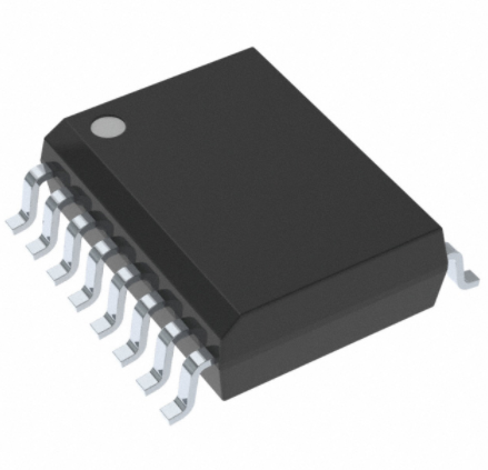
Available in SSOP16 package (150 mil)
© 2016 Genesys Logic, Inc. - All rights reserved.
GLI Confidential
Page 7
�GL823K Datasheet
CHAPTER 3
PIN ASSIGMENT
9 VDD
10 5V
11 GPIO
12 LED
13 VDDA
14 VSS
15 DP
16 DM
3.1 SSOP16 Pinout
GL823K
PMOS 8
D2 7
D3 6
CMD 5
CLK 4
D0 3
D1 2
VSS 1
SSOP-16 (150mil)
Figure 3.1 – SSOP 16 Pinout Diagram
© 2016 Genesys Logic, Inc. - All rights reserved.
GLI Confidential
Page 8
�GL823K Datasheet
3.2 Pin Description
Table 3.1 – Pin Description
Pin Name
PIN NO.
Type
Description
Power/Ground
VDDA
13
P
USB2.0 PHY 3.3V power source.
VDD
9
P
Digital 3.3V power source
VSS
1,14
P
Power ground
5V
10
P
VBUS 5V input
PMOS
8
P
Card power 200mA
USB PHY Interface
DP
15
A
USB 2.0 D+
DM
16
A
USB 2.0 D-
Memory Card Interface
CLK
4
O
SD/MS clock signal
CMD
5
B
SD command/MS BS signal
D0
3
B
SD/MS data 0 signal
D1
2
B
SD/MS data 1 signal
D2
7
B
SD/MS data 2 signal
D3
6
B
SD/MS data 3 signal
Others
GPIO
11
I, pu
LED
12
O
Notation:
Type
O
I
B
pu
pd
P
A
General Purpose I/O
Access LED
Output
Input
Bi-directional
internal pull-up when input
internal pull-down when input
Power / Ground
Analog
© 2016 Genesys Logic, Inc. - All rights reserved.
GLI Confidential
Page 9
�GL823K Datasheet
CHAPTER 4
BLOCK DIAGRAM
MHE
EPFIFO
EP0/EP3 FIFO
Regulator
5 to 3.3V
3.3 to 1.8V
SIE
SD 4bit I/F
BULK FIFO
OCCS
USB PHY
MSPRO 4bit
I/F
EHCI
RAM
Control
Register
8051
CORE
ROM
Table 4.1 – Functional Block Diagram
4.1 OCCS USB PHY
The USB 2.0 Transceiver Macrocell is the analog circuitry that handles the low level USB protocol and signaling,
and shifts the clock domain of the data from the USB 2.0 rate to one that is compatible with the general logic. On
chip clock source and no need of 12MHz Crystal Clock input.
4.2 SIE
The Serial Interface Engine, which contains the USB PID and address recognition logic, and other sequencing
and state machine logic to handle USB packets and transactions.
4.3 EPFIFO
Endpoint FIFO includes Control FIFO (FIFO0) and Bulk In/Out FIFO
EP0 FIFO
FIFO of control endpoint 0. It is 64-byte FIFO and used for endpoint 0 data transfer.
Interrupt FIFO
64-byte depth FIFO of endpoint 3 for status interrupt
Bulk FIFO It can be in the TX mode or RX mode:
1. It contains ping-pong FIFO (512 bytes each bank) for transmit/receive data continuously.
2. It can be directly accessed by micro-controller
4.4 MCU
8051 micro-controller inside.
8051 Core
Compliant with Intel 8051 high speed micro-controller
ROM
FW code on ROM
SRAM
Internal RAM area for MCU access
© 2016 Genesys Logic, Inc. - All rights reserved.
GLI Confidential
Page 10
�GL823K Datasheet
4.5 MHE
MIF
MCFIFO
Media Interface: SD/MMC
It can access by MCU for memory card short data packet.
4.6 Regulator
5V to 3.3V
3.3V to 1.8V
Band Gap Regulator for stable voltage supply for USB PHY, PMOS
For core logic and internal memory.
4.7 PMOS
On-Chip power MOSFETs for memory card power
© 2016 Genesys Logic, Inc. - All rights reserved.
GLI Confidential
Page 11
�GL823K Datasheet
CHAPTER 5
ELECTRICAL CHARACTERISTICS
5.1 Temperature Conditions
Table 5.1 – Temperature Conditions
Parameter
Value
Storage Temperature
-65C to +150 C
Operating Temperature
0C to +70 C
5.2 Operating Conditions
Table 5.2 – Operating Conditions
Parameter
Value
Supply Voltage
+4.75V to +5.25V
Ground Voltage
0V
5.3 DC Characteristics
Table 5.3 – DC Characteristics
Symbol
Parameter
Condition
Min.
Typ.
Max.
Unit
V5
Supply Voltage
5V power source
4.75
-
5.25
V
INORMAL
Idle current
-
45
-
mA
IACTIVE
Active current
-
50
-
mA
ISUS
Suspend current
-
0.3
-
mA
ICABLE
Cable mode current
-
0.15
-
mA
5.4 Memory Card Clock Frequency
Table 5.4 – SD/MMC Card Clock Frequency
Parameter
Description
Max.
Unit
FID
Clock frequency Identification Mode
187
KHz
FDS
Clock frequency Default Speed Mode
24
MHz
FHS
Clock frequency High Speed Mode
48
MHz
FUHS
Clock frequency Ultra High Speed Mode (SD only)
80
MHz
© 2016 Genesys Logic, Inc. - All rights reserved.
GLI Confidential
Page 12
�GL823K Datasheet
Table 5.5 – MS PRO Card Clock Frequency
Parameter
Description
Max.
Unit
FDS
Clock frequency Default Speed Mode
20
MHz
FMSP
Clock frequency MS PRO 4bit Mode
40
MHz
FMSPHG
Clock frequency MS PRO HG 4bit Mode
40
MHz
© 2016 Genesys Logic, Inc. - All rights reserved.
GLI Confidential
Page 13
�GL823K Datasheet
CHAPTER 6
PACKAGE DIMENSION
Internal
Version
No. GL823K
No.
AAAAAAAAAA
YWWXXXX
Date
Code
Lot Code
Figure 6.1 – SSOP 16 Pin Package (150 mil)
© 2016 Genesys Logic, Inc. - All rights reserved.
GLI Confidential
Page 14
�GL823K Datasheet
CHAPTER 7
ORDERING INFORMATION
Table 7.1 – Ordering Information
Part Number
Package
Green/Wire Material
Version
Status
GL823K-HCYXX
SSOP 16
Green Package + CU Wire
XX
Available
© 2016 Genesys Logic, Inc. - All rights reserved.
GLI Confidential
Page 15
�


 工商网监
湘ICP备2023018690号
工商网监
湘ICP备2023018690号
