GS9077
GS9077 HD-LINX® III SD-SDI Cable
Driver
Features
Description
•
SMPTE 344M and SMPTE 259M compliant
•
Dual coaxial cable driving outputs
The GS9077 is a high-speed BiCMOS integrated circuit
designed to drive one or two 75Ω co-axial cables.
•
Selectable power down mode
•
50Ω differential PECL input
•
Pb-free/Halogen-free/RoHS & WEEE compliant
•
Seamless interface to other HD-LINX® III family
products
•
Single 3.3V power supply operation
•
Operating temperature range: 0°C to 70°C
The GS9077 may drive data rates up to 540Mb/s and
provides a disable pin that may be used to power down the
output stage.
The GS9077 accepts a LVPECL level differential input that
may be AC coupled. External biasing resistors at the inputs
are not required.
Power consumption is typically 168mW using a 3.3V power
supply. The GS9077 is Pb-free, and the encapsulation
compound does not contain halogenated flame retardant.
Applications
•
SMPTE 344M and SMPTE 259M Coaxial Cable Serial
Digital Interfaces.
This component and all homogeneous subcomponents are
RoHS compliant.
BANDGAP REFERENCE AND BIASING CIRCUIT
DDI
DDI
INPUT
DIFFERENTIAL
PAIR
OUTPUT STAGE &
CONTROL
RSET
SDO
SDO
DISABLE
GS9077 Functional Block Diagram
GS9077
Final Data Sheet
GENDOC-044619
www.semtech.com
Rev.1
May 2019
1 of 14
Semtech
Proprietary & Confidential
�Revision History
Version
ECO/ECR
PCN
Date
Changes and/or Modifications
1
046907
—
May 2019
Updated document format.
0
144889
—
May 2007
New document.
Contents
1. Pin Out.................................................................................................................................................................3
1.1 Pin Assignment ...................................................................................................................................3
1.2 Pin Descriptions ..................................................................................................................................3
2. Electrical Characteristics................................................................................................................................4
2.1 Absolute Maximum Ratings ...........................................................................................................4
2.2 DC Electrical Characteristics ...........................................................................................................4
2.3 AC Electrical Characteristics ............................................................................................................5
3. Input / Output Circuits...................................................................................................................................6
4. Detailed Description.......................................................................................................................................7
4.1 Input Interfacing .................................................................................................................................7
4.2 Output Interfacing .............................................................................................................................7
4.2.1 Output Amplitude (RSET) ....................................................................................................8
4.2.2 Output Disable ........................................................................................................................8
4.3 Output Return Loss Measurement ...............................................................................................8
5. Application Information................................................................................................................................9
5.1 PCB Layout ............................................................................................................................................9
5.2 Typical Application Circuit ..............................................................................................................9
6. Package & Ordering Information ............................................................................................................ 10
6.1 Package Dimensions ...................................................................................................................... 10
6.2 Recommended PCB Footprint .................................................................................................... 11
6.3 Packaging Data ................................................................................................................................ 11
6.4 Solder Reflow Profiles .................................................................................................................... 12
6.5 Marking Diagram ............................................................................................................................. 13
6.6 Ordering Information ..................................................................................................................... 13
GS9077
Final Data Sheet
GENDOC-044619
www.semtech.com
Rev.1
May 2019
2 of 14
Semtech
Proprietary & Confidential
�1. Pin Out
DDI
1
DDI
2
NC
NC
NC
NC
1.1 Pin Assignment
16
15
14
13
12
SDO
11
SDO
GS9077
(top view)
VEE
3
10
NC
RSET
4
9
VCC
7
8
Center Pad
(bottom of package)
NC
RSVD
6
DISABLE
NC
5
Figure 1-1: 16-Pin QFN
1.2 Pin Descriptions
Table 1-1: Pin Descriptions
Pin Number
Name
Timing
Type
Description
1,2
DDI, DDI
Analog
Input
Serial digital differential input.
3
VEE
—
Power
Most negative power supply connection. Connect to GND.
4
RSET
Analog
Input
External output amplitude control resistor.
5,8,10,13,14,
15,16
NC
—
—
6
DISABLE
Non
Synchronous
Input
7
RSVD
—
Reserved
9
VCC
—
Power
Most positive power supply connection. Connect to +3.3V.
11,12
SDO,SDO
Analog
Output
Serial digital differential output.
—
Center Pad
—
Power
Connect to most negative power supply plane following the
recommendations in Recommended PCB Footprint on page 11.
GS9077
Final Data Sheet
GENDOC-044619
No Connect. Not bonded internally.
Serial output disable. When asserted LOW, the SDO/SDO output
driver is powered off. SDO/SDO will float to VCC through the pull-up
resistor.
Do not connect.
www.semtech.com
Rev.1
May 2019
3 of 14
Semtech
Proprietary & Confidential
�2. Electrical Characteristics
2.1 Absolute Maximum Ratings
Parameter
Value
Supply Voltage
-0.5V to 3.6 VDC
Input ESD Voltage
4kV
Storage Temperature Range
-50°C < TS < 125°C
Input Voltage Range (any input)
-0.3 to (VCC +0.3)V
Operating Temperature Range
0°C to 70°C
Solder Reflow Temperature
260°C
NOTE: Absolute Maximum Ratings are those values beyond which damage to the device may
occur. Functional operation under these conditions or at any other condition beyond those
indicated in the AC/DC Electrical Characteristic sections is not implied.
2.2 DC Electrical Characteristics
Table 2-1: DC Electrical Characteristics
VCC = 3.3V ±5%; TA = 0°C to 70°C, unless otherwise shown
Parameter
Supply Voltage
Power Consumption
Symbol
Conditions
Min
Typ
Max
Units
VCC
—
3.135
3.3
3.465
V
TA = 25°C,
SDO/SDO enabled
—
168
—
mW
TA = 25°C,
SDO/SDO disabled
—
96
—
mW
TA = 25°C,
SDO/SDO enabled
—
51
—
mA
TA = 25°C,
SDO/SDO disabled
—
29
—
mA
VCMOUT
Common mode
—
VCC - VOUT
—
V
VCMIN
Common mode
1.4 + VDDI/2
—
VCC - VDDI/2
V
VIH
IIH
很抱歉,暂时无法提供与“GS9077-CNTE3”相匹配的价格&库存,您可以联系我们找货
免费人工找货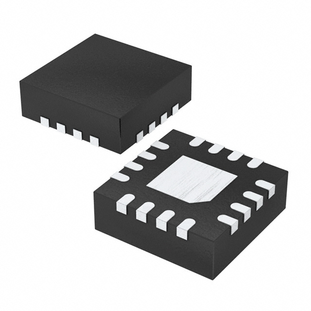


 工商网监
湘ICP备2023018690号
工商网监
湘ICP备2023018690号
