SC2446A
Dual-Phase, Single or Dual Output
Synchronous Step-Down Controller
POWER MANAGEMENT
Description
Features
2-Phase synchronous continuous conduction mode
The SC2446A is a high-frequency dual synchronous stepdown switching power supply controller. It provides outof-phase output gate signals. The SC2446A operates in
synchronous continuous-conduction mode. Both phases
are capable of maintaining regulation with sourcing or
sinking load currents, making the SC2446A suitable for
generating both VDDQ and the tracking VTT for DDR applications.
The SC2446A employs fixed frequency peak currentmode control for the ease of frequency compensation
and fast transient response.
The dual-phase step-down controllers of the SC2446A
can be configured to provide two individually controlled
and regulated outputs or a single output with shared
current in each phase. The Step-down controllers operate from an input of at least 4.7V and are capable of
regulating outputs as low as 0.5V
The step-down controllers in the SC2446A have the provision to sense inductor RDC voltage drop for current-mode
control. This sensing scheme eliminates the need of the
current-sense resistor and is more noise-immune than
direct sensing of the high-side or the low-side MOSFET
voltage. Precise current-sensing with sense resistor is
optional.
Individual soft-start and overload shutdown timer is included in each step-down controller. The SC2446A implements hiccup overload protection. In two-phase singleoutput configuration, the master timer controls the softstart and overload shutdown functions of both controllers.
for high efficiency step-down converters
Out of phase operation for low input current ripples
Output source and sink currents
Fixed frequency peak current-mode control
50mV/-75mV maximum current sense voltage
Inductive current-sensing for low-cost applications
Optional resistor current-sensing for precise current-limit
Dual outputs or 2-phase single output operation
Excellent current sharing between individual phases
Wide input voltage range: 4.7V to 16V
Individual soft-start, overload shutdown and enable
Duty cycle up to 88%
0.5V feedback voltage for low-voltage outputs
External reference input for DDR applications
Programmable frequency up to 1MHz per phase
External synchronization
Industrial temperature range
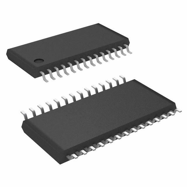
28-lead TSSOP lead free package. This product is
fully WEEE and RoHS compliant
Applications
Telecommunication power supplies
DDR memory power supplies
Graphic power supplies
Servers and base stations
Typical Application Circuit
V IN (1 2 V )
V IN G N D
C6
R 55
VO1
1 VDDO
L6
C 62
C 74
C 45
R 46
10
VO
11
CB
PVCC
U 10
VDDC
13
C 68
22
R 13
27
In te gra te d M O S F E T /D rive r
1
R CS-6
2
VO1GND
4
5
R 28
8
REF OUT (0. 5V)
7
R 29
R 45
C 29
R 47
3
16
C 40
VIN
BST2
GDH 1
GDH 2
23
19
20
9
C 72
C 73
13
C 67
R 52
24
9
VSSC
BST1
R 53
16
0
28 VSSO
26
25
VI
C7
R 49
GD L1
GD L2
16
U9
VDDC
VI
0
21
9
VSSC
VDDO
1
VO
10
CB
11
VO2
L5
C 65
R 14
C 23
C 75
VSSO 28
PGND
VPN 1
VPN 2
CS1+
CS2+
CS1-
CS2-
IN1-
IN2-
COMP1
COMP2
REF
REFIN
AGND
VIN 2
R osc
SYNC
AVCC
SS1/EN 1
R EFOU T
SS2/EN 2
18
R 50
In te gra te d M O S F E T /D rive r
14
R CS-5
13
VO2GND
12
11
10
REF OUT (0. 5V)
17
C 63
6
TP11
28
15
R 48
R 51
C 64
C 70
C 71
U3
Figure 1
Revision: November 9, 2005
SC2446A
REF OUT (0. 5V)
1
www.semtech.com
�SC2446A
POWER MANAGEMENT
Absolute Maximum Rating
Exceeding the specifications below may result in permanent damage to the device, or device malfunction. Operation outside of the parameters specified
in the Electrical Characteristics section is not implied. Exposure to Absolute Maximum rated conditions for extended periods of time may affect device
reliability.
Parameter
Symbol
Maximum Ratings
Units
AVCC
-0.3 to 16
V
VGDH1, VGDH2,VGDL1, VGDL2
-0.3 to 6
V
VIN1-,VIN2-
-0.3 to AVCC+0.3
V
VREF ,VREFOUT
-0.3 to 6
V
VREFIN
-0.3 to AVCC+0.3
V
VCOMP1,VCOMP2
-0.3 to AVCC+0.3
V
VCS1+,VCS1-,VCS2+,VCS2-
-0.3 to AVCC+0.3
V
VSYNC
-0.3 to AVCC+0.3
V
VSS1,VSS2
-0.3 to 6
V
Ambient Temperature Range
TA
-40 to 125
°C
Thermal Resistance Junction to Case (TSSOP-28)
θJ C
13
°C/W
Thermal Resistance Junction to Ambient (TSSOP-28)
θJ A
84
°C/W
Storage Temperature Range
TSTG
-60 to 150
°C
Lead Temperature (Soldering) 10 sec
TLEAD
260
°C
TJ
150
°C
Supply Voltage
Gate Outputs GDH1, GDH2, GDL1, GDL2 voltages
IN1-, IN2- Voltages
REFOUT Voltages
REF, REFIN Voltage
COMP1, COMP2 Voltages
CS1+, CS1-, CS2+ and CS2- Voltages
SYNC Voltage
SS1/EN1 AND SS2/EN2 Voltages
Maximum Junction Temperature
Electrical Characteristics
Unless specified: AVCC = 12V, SYNC = 0, ROSC = 51.1kΩ, -40°C < TA = TJ < 125°C
Parameter
Symbol
Conditions
Min
Typ
Max
Units
4.5
4.7
V
Undervoltage Lockout
AVCC Start Threshold
AVCCTH
AVCC Start Hysteresis
AVCCHYST
AVCC Operating Current
ICC
AVCC Quiescent Current in UVLO
AVCC Increasing
0.2
AVCC= 12V
8
AVCC = AVCCTH - 0.2V
V
15
2.5
mA
mA
Channel 1 Error Amplifier
Input Common-Mode Voltage Range
(Note 1)
0
3
V
Inverting Input Voltage Range
(Note 1)
0
AVCC
V
Input Offset Voltage
0 ~ 70° C
1
±3
mV
Non-Inverting Input Bias Current
IREF
-100
-250
nA
Inverting Input Bias Current
IIN1-
-100
-250
nA
Amplifier Transconductance
GM1
260
μΩ−1
Amplifier Open-Loop Gain
aOL1
65
dΒ
5
MHz
2.2
V
Amplifier Unity Gain Bandwidth
Minimum COMP1 Switching Threshold
© 2005 Semtech Corp.
V C S 1+ = V C S 1- = 0
VSS1 Increasing
2
www.semtech.com
�SC2446A
POWER MANAGEMENT
Electrical Characteristics (Cont.)
Unless specified: AVCC = 12V, SYNC = 0, ROSC = 51.1kΩ, -40°C < TA = TJ < 125°C
Parameter
Symbol
Conditions
Min
Typ
Max
Units
Amplifier Output Sink Current
VIN1- = 1V, VCOMP1 = 2.5V
16
μA
Amplifier Output Source Current
VIN1- = 0, VCOMP1 = 2.5V
12
μA
Channel 2 Error Amplifier
Input Common-mode Voltage Range
(Note 1)
0
3
V
Inverting Input Voltage Range
(Note 1)
0
AVCC
V
Input Offset Voltage
0 ~ 70° C
1.5
±3
mV
Non-inverting Input Bias Current
IIN2+
-150
-380
nA
Inverting Input Bias Current
IIN2-
-100
-250
nA
Inverting Input Voltage for 2-Phase Single
Output Operation
2.5
V
Amplifier Transconductance
GM2
260
μΩ−1
Amplifier Open-Loop Gain
aOL2
65
dΒ
5
MHz
Amplifier Unity Gain Bandwidth
Minimum COMP2 Switching Threshold
V C S 2+ = V C S 2- = 0
VSS2 Increasing
2.2
V
Amplifier Output Sink Current
VCOMP2 = 2.5V
16
μA
Amplifier Output Source Current
VCOMP2 = 2.5V
12
μA
Oscillator
Channel Frequency
fCH1, fCH2
Synchronizing Frequency
0 ~ 70° C
(Note 1)
SYNC Input High Voltage
450
500
ISYNC
Channel Maximum Duty Cycle
DMAX1, DMAX2
Channel Minimum Duty Cycle
DMIN1, DMIN2
KHz
2.1fCH
KHz
1.5
V
SYNC Input Low Voltage
SYNC Input Current
550
VSYNC = 0.2V
VSYNC = 2V
0.5
V
1
50
μA
88
%
0
%
AVCC - 1
V
Current-limit Comparators
Input Common-Mode Range
0
Cycle-by-cycle Peak Current Limit
VILIM1+,
VILIM2+
Valley Current Overload Shutdown
Threshold
VILIM1-, VILIM2-
VCS1- = VCS2- = 0.5V,
Sourcing Mode, 0 ~ 70° C
40
50
60
mV
VCS1- = VCS2- = 0.5V,
Sinking Mode, 0 ~ 70° C
-60
-75
-90
mV
Positive Current-Sense Input Bias Current
ICS1+, ICS2+
V C S 1+ = V C S 1- = 0
V C S 2- = V C S 2- = 0
-0.7
-2
μA
Negative Current-Sense Input Bias
Current
ICS1-, ICS2-
V C S 1+ = V C S 1- = 0
V C S 2+ = V C S 2- = 0
-0.7
-2
μA
© 2005 Semtech Corp.
3
www.semtech.com
�SC2446A
POWER MANAGEMENT
Electrical Characteristics (Cont.)
Unless specified: AVCC = 12V, SYNC = 0, ROSC = 51.1kΩ, -40°C < TA = TJ < 125°C
Parameter
Symbol
Conditions
Min
Typ
Max
Units
PWM Outputs
Peak Source Current
GDL1, GDL2,
GDH1, GDH2
AVCC = 12V
4
mA
Peak Sink Current
GDL1, GDL2,
GDH1, GDH2
AVCC = 12V
3
mA
Output High Voltage
Source IO = 1.2mA, 0 ~ 70° C
3.95
5
V
Output Low Voltage
Sink IO = 1mA
0
0.4
V
Minimum On-Time
TA = 25°C
120
ns
VSS1 = VSS2 = 1.5V
1.8
μA
Overload Latchoff Enabling
Soft-Start Voltage
VSS1 and VSS2 Increasing
3.2
V
Overload Latchoff
IN1- Threshold
VSS1 = 3.8V, VIN1-Decreasing
0.5VREF
V
Overload Latchoff
IN2- Threshold
VSS2 = 3.8V, VIN2-Decreasing
0.5 X
VREFIN
V
1.2
μA
Soft-Start, Overload Latchoff and Enable
Soft-Start Charging Current
Soft-Start Discharge Current
ISS1, ISS2
VIN1-= 0.5VREF,
ISS1(DIS), ISS2(DIS) VIN2-= 0.5VREFIN ,
VSS1 = VSS2 = 3.8V
Overload Latchoff Recovery
Soft-Start Voltage
VSSRCV1,
VSSRCV2
VSS1 and VSS2 Decreasing
PWM Output Disable SS/EN
Voltage
0.3
0.5
0.7
0.8
PWM Output Enable SS/EN
Voltage
0.7
V
V
1.2
1.5
V
500
505
mV
Internal 0.5V Reference Buffer
Output Voltage
VREFOUT
IREFOUT = -1mA, 0- °C < TA = TJ < 70°C
Load Regulation
0 < IREFOUT < -5mA
Line Regulation
AVCCTH < AVCC < 15V, IREFOUT = -1mA
495
0.05
%/mA
0.02%
%V
Notes:
(1) Guaranteed by design not tested in production.
(2) This device is ESD sensitive. Use of standard ESD handling precautions is required.
© 2005 Semtech Corp.
4
www.semtech.com
�SC2446A
POWER MANAGEMENT
Pin Configurations
Ordering Information
Device
TOP VIEW
SC2446AITSTRT(1)(2)
CS1+
1
28
CS1-
2
27
VPN1
ROSC
3
26
BST1
IN1-
4
25
GDH1
COMP1
5
24
GDL1
SYNC
6
23
PVCC
AGND
7
22
PGND
REF
8
21
GDL2
REFOUT
9
20
GDH2
REFIN
10
19
BST2
COMP2
11
18
VPN2
IN2-
12
17
VIN2
CS2-
13
16
AVCC
CS2+
14
15
SS2/EN2
S C 2446A E V B
SS1/EN1
P ackag e
Temp. Range( TA)
TSSOP-28
-40 to 125°C
Evaluation Board
Notes:
(1) Only available in tape and reel packaging. A reel
contains 2500 devices for TSSOP package.
(2) Lead free product. This product is fully WEEE and
RoHS compliant.
(28 Pin TSSOP)
Figure 2
© 2005 Semtech Corp.
5
www.semtech.com
�SC2446A
POWER MANAGEMENT
Pin Descriptions
TSSOP Package
Pin
Pin Name
1
C S 1+
The Non-inverting Input of the Current-sense Amplifier/Comparator for the Controller 1.
2
C S 1-
The Inverting Input of the Current-sense Amplifier/Comparator for the Controller 1. Normally
tied to the output of the converter.
3
ROSC
An external resistor connected from this pin to GND sets the oscillator frequency.
4
IN1-
5
COMP1
6
SYNC
Edge-triggered Synchronization Input. When not synchronized, tie this pin to a voltage above
1.5V or the ground. An external clock (frequency > frequency set with ROSC) at this pin
synchronizes the controllers.
7
AGND
Analog Signal Ground.
8
REF
9
REFOUT
10
REFIN
11
COMP2
The Error Amplifier Output for Step-down Controller 2. This pin is used for loop compensation.
12
IN2-
Inverting Input of the Error Amplifier for the Step-down Controller 2. Tie an external resistive
divider between output2 and the ground for output voltage sensing. Tie to AVCC for two-phase
single output applications
13
C S 2-
The Inverting Input of the Current-sense Amplifier/Comparator for the Controller 2. Normally
tied to the output of the converter.
14
C S 2+
The Non-inverting Input of the Current-sense Amplifier/Comparator for the Controller 2
15
SS2/EN2
16
AVCC
17
VIN2
No connection.
18
VPN2
No connection.
19
BST2
No connection.
20
GDH2
PWM Output for the High-side N-channel MOSFET of Output 2.
© 2005 Semtech Corp.
Pin Function
Inverting Input of the Error Amplifier for the Step-down Controller 1. Tie an external resistive
divider between OUTPUT1 and the ground for output voltage sensing.
The Error Amplifier Output for Step-down Controller 1. This pin is used for loop compensation.
The non-inverting input of the error amplifier for the step down converter 1.
Buffered output of the internal reference voltage 0.5V.
An external Reference voltage is applied to this pin.The non-inverting input of the error
amplifier for the step-down converter 2 is internally connected to this pin.
An external capacitor tied to this pin sets (i) the soft-start time (ii) output overload latch off time
for step-down converter 2. Pulling this pin below 0.7V shuts off the gate drivers for the second
controller. Leave open for two-phase single output applications.
Power Supply Voltage for the Analog Portion of the Controllers.
6
www.semtech.com
�SC2446A
POWER MANAGEMENT
Pin Descriptions
Pin
Pin Name
21
GDL2
Logic Enable gate drive signal for Output 2.
22
PGND
No connection.
23
PVC C
No connection.
24
GDL1
Logic Enable gate drive signal for Output 1.
25
GDH1
PWM Output for the High-side N-channel MOSFET of Output 1.
26
BST1
No connection.
27
VPN1
No connection.
28
SS1/EN1
© 2005 Semtech Corp.
Pin Function
An external capacitor tied to this pin sets (i) the soft-start time (ii) output overload latch off time
for buck converter 1. Pulling this pin below 0.7V shuts off the gate drivers for the first controller.
7
www.semtech.com
�SC2446A
POWER MANAGEMENT
Block Diagram
SYNC
CLK2
6
FREQUENCY
DIVIDER
CLK
OSCILLATOR
ROSC
3
COMP1
AVCC
1.25V
CLK1
16
REFERENCE
BST1
26
SLOPE COMP
0.5V
5
IN1-
-
4
REF
8
+
GDH1
25
SLOPE2
EA1
-
R
+
S
PWM1
Q
VPN1
27
SLOPE1
CS1+
1
+
+
ISEN1
CS12
-
Σ
UV
+
24
Soft-Start
And
Overload
Hiccup
Control 1
+
ILIM1+
I
-
50mV
OCN1
-
ILIM1 -
75mV
REFOUT
OL1
PGND
DSBL1
22
SS1/EN1
28
VIN2
0.5 (REFOUT)
+
+
9
GDL1
17
0.5V
-
PVCC
UVLO
4.3/4.5V
COMP2
AGND
7
+
11
-
SEL
+
IN212
REFIN
10
+
Y
CLK2
0.5 (REFIN)
EA2
+
+
ISEN2
-
-
+
S
Q
VPN2
UV
+
75mV
GDL2
21
Σ
ILIM2
I
50mV
19
18
+
-
BST2
20
R
PWM2
CS2+
SEL
GDH2
ANALOG
SWITCH
SLOPE2
13
A
B
1.8V
14
CS2-
23
OCN2
Soft-Start
And
Overload
Hiccup
Control 2
OL2
DSBL2
SS2/EN2
15
ILIM2 -
+
0.5 (REFIN)
Figure 3. SC2446A Block Diagram
© 2005 Semtech Corp.
8
www.semtech.com
�SC2446A
POWER MANAGEMENT
Block Diagram
OCN
IN-
-
0.5(VREFOUT)
/ 0.5(VREFIN )
S
+
Q
1.8μΑ
OL
R
SS/EN
0.5V/3.2V
DSBL
UVLO
0.8V/1.2V
3μΑ
Figure 4. Soft-Start and Overload Hiccup Control Circuit
© 2005 Semtech Corp.
9
www.semtech.com
�SC2446A
POWER MANAGEMENT
Application Information
SC2446A consists of two current-mode synchronous
buck controllers with many integrated functions. By
proper application circuitry configuration, SC2446A can
be used to generate
1) two independent outputs from a common input or
two different inputs or
2) dual phase output with current sharing,
3) current sourcing/sinking from common or separate
inputs as in DDR (I and II) memory application.
The application information related to the converter
design using SC2446A is described in the following.
Step-down Converter
Starting from the following step-down converter
specifications,
Input voltage range: Vin ∈ [ Vin,min , Vin,max ]
Input voltage ripple (peak-to-peak): ΔVin
Output voltage: Vo
Output voltage accuracy: ε
Output voltage ripple (peak-to-peak): ΔVo
Nominal output (load) current: Io
Maximum output current limit: Io,max
Output (load) current transient slew rate: dIo (A/s)
Circuit efficiency: η
Selection criteria and design procedures for the following
are described.
1) output inductor (L) type and value,
2) output capacitor (Co) type and value,
3) input capacitor (Cin) type and value,
4) power MOSFET’s,
5) current sensing and limiting circuit,
6) voltage sensing circuit,
7) loop compensation network.
Operating Frequency (fs)
The switching frequency in the SC2446A is userprogrammable. The advantages of using constant
frequency operation are simple passive component
selection and ease of feedback compensation. Before
setting the operating frequency, the following trade-offs
should be considered.
1)
2)
3)
4)
5)
For a given output power, the sizes of the passive
components are inversely proportional to the switching
frequency, whereas MOSFETs/Diodes switching losses
are proportional to the operating frequency. Other issues
such as heat dissipation, packaging and the cost issues
are also to be considered. The frequency bands for signal
transmission should be avoided because of EM
interference.
Minimum Switch On Time Consideration
In the SC2446A the falling edge of the clock turns on
the top MOSFET gate. The inductor current and the
sensed voltage ramp up. After the sensed voltage crosses
a threshold determined by the error amplifier output, the
top MOSFET gate is turned off. The propagation delay
time from the turn-on of the controlling FET to its turnoff is the minimum switch on time. The SC2446A has a
minimum on time of about 120ns at room temperature.
This is the shortest on interval of the controlling FET. The
controller either does not turn on the top MOSFET at all
or turns it on for at least 120ns.
For a synchronous step-down converter, the operating
duty cycle is VO/VIN. So the required on time for the top
MOSFET is VO/(VINfs). If the frequency is set such that
the required pulse width is less than 120ns, then the
converter will start skipping cycles. Due to minimum on
time limitation, simultaneously operating at very high
switching frequency and very short duty cycle is not
practical. If the voltage conversion ratio VO/VIN and hence
the required duty cycle is higher, the switching frequency
can be increased to reduce the sizes of passive
components.
There will not be enough modulation headroom if the on
time is simply made equal to the minimum on time of the
SC2446A. For ease of control, we recommend the
required pulse width to be at least 1.5 times the minimum
on time.
Passive component size
Circuitry efficiency
EMI condition
Minimum switch on time and
Maximum duty ratio
© 2005 Semtech Corp.
10
www.semtech.com
�SC2446A
POWER MANAGEMENT
Application Information (Cont.)
Setting the Switching Frequency
The switching frequency is set with an external resistor
connected from Pin 3 to the ground. The set frequency
is inversely proportional to the resistor value (Figure 5).
800
700
fs (kHz)
600
500
400
300
200
100
0
0
50
100
150
200
250
Rosc (k Ohm)
The followings are to be considered when choosing
inductors.
a) Inductor core material: For high efficiency applications
above 350KHz, ferrite, Kool-Mu and polypermalloy
materials should be used. Low-cost powdered iron cores
can be used for cost sensitive-applications below 350KHz
but with attendant higher core losses.
b) Select inductance value: Sometimes the calculated
inductance value is not available off-the-shelf. The
designer can choose the adjacent (larger) standard
inductance value. The inductance varies with
temperature and DC current. It is a good engineering
practice to re-evaluate the resultant current ripple at
the rated DC output current.
c) Current rating: The saturation current of the inductor
should be at least 1.5 times of the peak inductor current
under all conditions.
Output Capacitor (Co) and Vout Ripple
Figure 5. Free running frequency vs. ROSC.
Inductor (L) and Ripple Current
Both step-down controllers in the SC2446A operate in
synchronous continuous-conduction mode (CCM)
regardless of the output load. The output inductor
selection/design is based on the output DC and transient
requirements. Both output current and voltage ripples
are reduced with larger inductors but it takes longer to
change the inductor current during load transients.
Conversely smaller inductors results in lower DC copper
losses but the AC core losses (flux swing) and the winding
AC resistance losses are higher. A compromise is to
choose the inductance such that peak-to-peak inductor
ripple-current is 20% to 30% of the rated output load
current.
Assuming that the inductor current ripple (peak-to-peak)
value is δ*Io, the inductance value will then be
L=
Vo (1 − D)
.
δIo fs
The peak current in the inductor becomes (1+δ/2)*Io
and the RMS current is
IL,rms = Io 1 +
© 2005 Semtech Corp.
δ2
.
12
The output capacitor provides output current filtering in
steady state and serves as a reservoir during load
transient. The output capacitor can be modeled as an
ideal capacitor in series with its parasitic ESR (Resr) and
ESL (Lesl) (Figure 6).
Co
Lesl
Resr
Figure 6. An equivalent circuit of Co.
If the current through the branch is ib(t), the voltage
across the terminals will then be
t
di ( t )
1
v o ( t ) = Vo +
ib ( t )dt + L esl b + R esr ib ( t ).
dt
Co 0
∫
This basic equation illustrates the effect of ESR, ESL
and Co on the output voltage.
The first term is the DC voltage across Co at time t=0.
The second term is the voltage variation caused by the
11
www.semtech.com
�SC2446A
POWER MANAGEMENT
Application Information (Cont.)
charge balance between the load and the converter
output. The third term is voltage ripple due to ESL and
the fourth term is the voltage ripple due to ESR. The
total output voltage ripple is then a vector sum of the
last three terms.
The voltage rating of aluminum capacitors should be at
least 1.5Vo. The RMS current ripple rating should also be
greater than
Since the inductor current is a triangular waveform with
peak-to-peak value δ*Io, the ripple-voltage caused by
inductor current ripples is
Usually it is necessary to have several capacitors of the
same type in parallel to satisfy the ESR requirement. The
voltage ripple cause by the capacitor charge/discharge
should be an order of magnitude smaller than the voltage
ripple caused by the ESR. To guarantee this, the
capacitance should satisfy
Δv C ≈
δIo
,
8C o fs
δIo
2 3
the ripple-voltage due to ESL is
Δv ESL
and the ESR ripple-voltage is
Δv ESR = R esr δIo .
Aluminum capacitors (e.g. electrolytic, solid OS-CON,
POSCAP, tantalum) have high capacitances and low
ESL’s. The ESR has the dominant effect on the output
ripple voltage. It is therefore very important to minimize
the ESR.
When determining the ESR value, both the steady state
ripple-voltage and the dynamic load transient need to be
considered. To keep the steady state output ripple-voltage
< ΔVo, the ESR should satisfy
R esr1 <
ΔVo
.
δIo
To limit the dynamic output voltage overshoot/
undershoot within α (say 3%) of the steady state output
voltage) from no load to full load, the ESR value should
satisfy
R esr 2 <
αVo
.
Io
Then, the required ESR value of the output capacitors
should be
Resr = min{Resr1,Resr2 }.
© 2005 Semtech Corp.
Co >
δI
= L esl fs o ,
D
.
10
.
2πfsR esr
In many applications, several low ESR ceramic capacitors
are added in parallel with the aluminum capacitors in
order to further reduce ESR and improve high frequency
decoupling. Because the values of capacitance and ESR
are usually different in ceramic and aluminum capacitors,
the following remarks are made to clarify some practical
issues.
Remark 1: High frequency ceramic capacitors may not
carry most of the ripple current. It also depends on the
capacitor value. Only when the capacitor value is set
properly, the effect of ceramic capacitor low ESR starts
to be significant.
For example, if a 10μF, 4mΩ ceramic capacitor is
connected in parallel with 2x1500μF, 90mΩ electrolytic
capacitors, the ripple current in the ceramic capacitor is
only about 42% of the current in the electrolytic
capacitors at the ripple frequency. If a 100μF, 2mΩ
ceramic capacitor is used, the ripple current in the
ceramic capacitor will be about 4.2 times of that in the
electrolytic capacitors. When two 100μF, 2mΩ ceramic
capacitors are used, the current ratio increases to 8.3.
In this case most of the ripple current flows in the
ceramic decoupling capacitor. The ESR of the ceramic
capacitors will then determine the output ripple-voltage.
Remark 2: The total equivalent capacitance of the filter
bank is not simply the sum of all the paralleled capacitors.
The total equivalent ESR is not simply the parallel
combination of all the individual ESR’s either. Instead
they should be calculated using the following formulae.
12
www.semtech.com
�SC2446A
POWER MANAGEMENT
Application Information (Cont.)
2
C eq (ω) :=
2
(R1a + R1b )2 ω2C1a C1b + (C1a + C1b )2
2
2
(R1a C1a + R1b C1b )ω2 C1a C1b + (C1a + C1b )
2
R eq (ω) :=
2
2
2
R1aR1b (R1a + R1b )ω2C1a C1b + (R1b C1b + R1a C1a )
2
2
(R1a + R1b )2 ω2 C1a C1b + (C1a + C1b )2
where R 1a and C 1a are the ESR and capacitance of
electrolytic capacitors, and R1b and C1b are the ESR and
capacitance of the ceramic capacitors respectively.
(Figure 7)
C1a
R1a
C1b
R1b
Ceq
Req
Figure 8. A simple model for the converter input
In Figure 8 the DC input voltage source has an internal
impedance Rin and the input capacitor Cin has an ESR of
Resr. MOSFET and input capacitor current waveforms, ESR
voltage ripple and input voltage ripple are shown in Figure
9.
Figure 7. Equivalent RC branch.
Req and Ceq are both functions of frequency. For rigorous
design, the equivalent ESR should be evaluated at the
ripple frequency for voltage ripple calculation when both
ceramic and electrolytic capacitors are used. If R1a = R1b
= R1 and C1a = C1b = C1, then Req and Ceq will be frequencyindependent and
Req = 1/2 R1 and Ceq = 2C1.
Input Capacitor (Cin)
The input supply to the converter usually comes from a
pre-regulator. Since the input supply is not ideal, input
capacitors are needed to filter the current pulses at the
switching frequency. A simple buck converter is shown in
Figure 8.
Figure 9. Typical waveforms at converter input.
It can be seen that the current in the input capacitor
pulses with high di/dt. Capacitors with low ESL should be
used. It is also important to place the input capacitor
close to the MOSFETs on the PC board to reduce trace
inductances around the pulse current loop.
The RMS value of the capacitor current is approximately
ICin = Io D[(1 +
© 2005 Semtech Corp.
13
δ2
D
D
)(1 − )2 + 2 (1 − D) ].
12
η
η
www.semtech.com
�SC2446A
POWER MANAGEMENT
Application Information (Cont.)
The power dissipated in the input capacitors is then
Let the duty ratio and output current of Channel 1 and
Channel 2 be D1, D2 and Io1, Io2, respectively.
PCin = ICin2Resr.
If D1


 工商网监
湘ICP备2023018690号
工商网监
湘ICP备2023018690号
