SC2599
Low Voltage DDR
Termination Regulator
POWER MANAGEMENT
Features
Description
The SC2599 is designed to meet the latest JEDEC specification for low power DDR3 and DDR4, while also supporting DDR and DDR2. The SC2599 regulates up to + 3A for
VTT and up to + 40mA for VREF.
Input to linear regulator (VIN): 1.0V to 3.6V
Output (VTT): 0.5V to 1.8V
Bias Voltage (VDD): 2.35V to 3.6V
Up to 3A sink or source from VTT for DDR through
DDR4
+ 1% over temperature (with respect to VDDQ/2, including internal resistor divider variation) VREF and
VTT
Logic-level enable input
Built in soft-start
Thermal shutdown with auto-restart
Over current protection
Minimal output capacitance
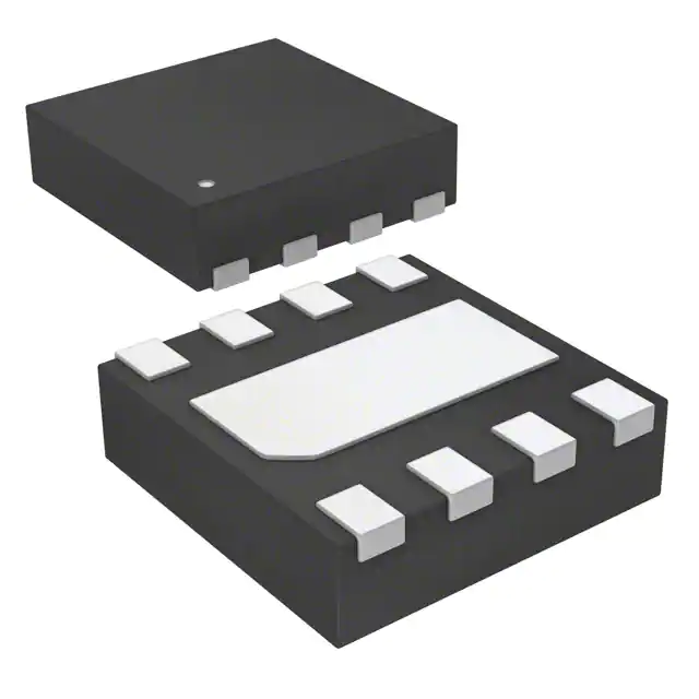
Package: MLPD8 - 2mm x 2mm x 0.6mm
Applications
The SC2599 also provides an accuracy of +1% over temperature (which takes into account the internal resistor
divider) for VREF and VTT for the memory controller and
DRAM.
SC2599 protection features include thermal shutdown
with auto-restart for VTT and over-current limit for both
VTT and VREF.
Under-Voltage-Lock-Out circuits are included to ensure
that the output is off when the bias voltage falls below its
threshold, and that the part behaves elegantly in powerup or power-down.
The low external parts count combined with industry
leading specifications make SC2599 an attractive solution
for DDR through DDR4 termination.
DDR Memory Termination
Typical Application Circuit
C VDD
C IN
1μF
2 x 1 0μF
VDDQ
VDD
V IN
VDDQ
VTT
VTTS
C VTT
VREF
EN
PAD
GND
C V R E F (1 )
3 x1 0 μF
0 .1 μF
Note:
(1) This component is optional.
Rev. 2.0
1
�SC2599
Pin Configuration
VDD
1
V IN
2
VTT
3
GND
4
Ordering Information
T h e rm a l
PAD
8
VDDQ
7
VREF
6
VTTS
5
EN
Device
Package
SC2599ULTRC(1)(2)
MLPD8
SC2599EVB
Evaluation Board
Notes:
(1) Available in tape and reel only. A reel contains 3000 devices.
(2) Lead-free packaging only. Device is WEEE and RoHS compliant
and halogen-free.
MLPD8 - 2mm x 2mm x 0.6mm
Marking Information
C 99
Yw
nnn = Part Number (Example: C99)
Yw = Datecode
2
�SC2599
Absolute Maximum Ratings
Thermal Information
VIN (V) . . . . . . . . . . . . . . . . . . . . . . . . . . . . . . . . . . . . . -0.3 to 4.3
Thermal Resistance, Junction to Ambient(2) (°C/W) . . . 57
VDD to GND (V) . . . . . . . . . . . . . . . . . . . . . . . . . . . . -0.3 to 4.3
Thermal Resistance, Junction to Ambient(3) (°C/W) . . . 45
VTT to GND (V) . . . . . . . . . . . . . . . . . . . . . . . . . . . . -0.3 to VDD
Maximum Junction Temperature (°C) . . . . . . . . . . . . . . +150
EN (V) . . . . . . . . . . . . . . . . . . . . . . . . . . . . . . . . . . . . . -0.3 to 6.0
Storage Temperature Range (°C) . . . . . . . . . . . . -65 to +150
Other pins . . . . . . . . . . . . . . . . . . . . . . . . . . . . . . . . . -0.3 to 4.3
Peak IR Reflow Temperature (10s to 30s) (°C) . . . . . . . +260
(1)
2.5
(1)
1
ESD Protection Level (HBM) (kV) . . . . . . . . . . .
ESD Protection Level (CDM) (kV). . . . . . . . . . .
Exceeding the above specifications may result in permanent damage to the device or device malfunction. Operation outside of the parameters
specified in the Electrical Characteristics section is not recommended.
Notes:
(1) HBM: tested according to ANSI/ESDA/JEDEC JS-001. CDM: tested according to JESD-C101E.
(2) Calculated from package in still air, mounted to 3 x 4.5 (in), 4 layer FR4 PCB with thermal vias under the exposed pad per JESD51 standards.
(3) Based upon lab measurement on EVB board: 3 x 2 (in), 4 layer FR4 PCB with thermal vias under the exposed pad.
Electrical Characteristics
Unless otherwise noted TJ = -40 to +125°C, VIN = 1.2V, VDD = 3.3V . Typical values are at TA = 25°C.
Parameter
Symbol
Conditions
Min
Typ
Max
Units
Input Supplies
LDO Supply Voltage
VIN
1
3.6
V
VDD Supply Voltage
VDD
2.35
3.6
V
Measured at VDD pin, rising edge
2.0
2.25
Measured at VDD pin, falling edge
1.95
2.15
VDD UVLO Threshold
V
VDD UVLO Hysteresis
0.1
Quiescent Current for VDD
IQ
Shutdown Current for VDD
IQSD
V
Load =0A, EN = High, VVDDQ > 1V
415
700
μA
Load =0A, EN = Low, VVDDQ > 1V, IREF = 0A
160
400
μA
Load =0A, EN = Low, VVDDQ = 0V, IREF = 0A
100
160
μA
Quiescent Current for VIN
IIN
Load =0A, EN = High
3
30
μA
Shutdown Current for VIN
IINSD
Load =0A, EN = Low
3
20
μA
0.5
1.8
V
-1
+1
%
VTT Output
Output Voltage Range
Output Voltage Tolerance with
respect to VDDQ/2
VTT
Load = 0A, VTT = 0.5V to 1.8V
3
�SC2599
Electrical Characteristics (continued)
Parameter
Load Regulation
Symbol
Conditions
Min
Typ
Max
Units
-2A < Load < 2A
-25
+25
mV
High-Side MOSFET (source), Load = 0.1A
40
100
150
Low-Side MOSFET (sink), Load = 0.1A
50
140
300
On-Resistance
Discharge MOSFET On-Resistance
mΩ
EN = Low
8
Ω
Reference Input/Output
VDDQ Voltage Range
1
3.6
V
VDDQ Input Bias Current
0
10
μA
-1
1
%
Tolerance with respect to VDDQ/2
Load = 0A, VREF = 0.5V to 1.8V
VREF Source Current Limit
40
VREF Sink Current Limit
- 40
mA
Protection
Thermal Shutdown Threshold
160
0
Thermal Restart Hysteresis
20
0
4.3
A
40
μs
Output Current Limit Threshold
Ambient Temperature: 25 0C
3.7
C
C
Soft-Start
VTT Soft-Start Time
From EN = High to V TT = 90% VREF
Logic
EN = High
1.7
EN Logic Threshold
V
EN = Low
EN Input Current
0.3
-1
1
μA
4
�SC2599
Block Diagram
T h e rm a l
S h u td o w n
VDD
1
EN
5
VDDQ
8
U VLO
2
V IN
3
VTT
4
GND
6
VTTS
S o ft-S ta rt
R
+
R
D R IV E R
L O G IC
-
+
-
EN\
VREF
7
Pin Descriptions
Pin #
Pin Name
Pin Function
1
VDD
Input bias voltage — 2.35V to 3.6V . Connect a ceramic capacitor from this pin to GND.
2
VIN
LDO input range — 1V to 3.6V. Connect ceramic capacitors from this pin to GND.
3
VTT
Output of the linear regulator. Connect ceramic capacitors from this pin to GND.
4
GND
Ground reference for the IC.
5
EN
Logic input to enable or disable the VTT output. If EN pin is grounded to shut down the linear regulator,
VREF remains active.
6
VTTS
VTT output sense input. Connect VTTS to the output at the output capacitor to implement remote sense.
7
VREF
The reference output, equal to one half of VDDQ. Connect a 100nF capacitor from this pin to GND.
8
VDDQ
External reference input; range 1V to 3.6V.
PAD
GND
Thermal pad. This pad must be connected to GND. For optimal heat sinking, connect to the GND plane using multiple vias.
5
�SC2599
Detailed Application Circuit
C1
4 GND
PAD
5 EN
EN
C2
C3
VTT
VTT 3
V IN 2
C4
6 VTTS
VDD 1
7 VREF
VDDQ 8
C7
V IN
3 .3 V
C6
VREF
C5
R1
100 O hm
C8
Bill Of Materials
Reference Designator
Description
Value
Part Number
Manufacture
C1, C2, C3, C4, C5,
Ceramic Capacitor
10uF/0805/X7R
GRM21BR71A106KE51
Murata
C6
Ceramic Capacitor
1uF/0603/X7R
GRM188R71A105KA61D
Murata
C7, C8
Ceramic Capacitor
0.1uF/0603/X7R
GRM188R71H104KA93D
Murata
6
�SC2599
Typical Characteristics
Characteristics in this section are based upon the detailed application circuit on page 6.
0.6V VREF Regulation Sink/Source
0.6V VTT Regulation Sink/Source
VIN = 1.2V, VDDQ = 1.2V, VDD = 3.3V
VIN = 1.2V, VDDQ = 1.2V, VDD = 3.3V
0.620
Sink
Source
0.610
VREF Regulation (V)
VTT Regulation (V)
Sink
250C
850C
-400C
0.600
-3
-2
0.580
0.580
1
2
-0.05 -0.04 -0.03 -0.02 -0.01
3
VTT Current (A)
VREF Regulation (V)
VTT Regulation (V)
Sink
Source
0.760
250C
850C
-400C
0.750
Source
250C
850C
-400C
0.730
0
1
2
3
0
0.01
0.02
0.03
0.04
0.05
VREF Current (A)
0.9V VREF Regulation Sink/Source
VIN = 1.8V, VDDQ = 1.8V, VDD = 3.3V
VIN = 1.8V, VDDQ = 1.8V, VDD = 3.3V
Sink
Source
VREF Regulation (V)
0.920
VTT Regulation (V)
0.770
-0.05 -0.04 -0.03 -0.02 -0.01
0.9V VTT Regulation Sink/Source
250C
850C
-400C
0.910
0.900
0.880
0
VTT Current (A)
0.920
Source
250C
850C
-400C
0.910
0.900
0.890
0.890
-1
0.05
0.740
VTT Current (A)
-2
0.04
0.750
0.730
-3
0.03
0.760
0.740
Sink
0.02
VIN = 1.5V, VDDQ = 1.5V, VDD = 3.3V
0.770
-1
0.01
0.75V VREF Regulation Sink/Source
VIN = 1.5V, VDDQ = 1.5V, VDD = 3.3V
-2
0
VREF Current (A)
0.75V VTT Regulation Sink/Source
-3
250C
850C
-400C
0.600
0.590
0
Source
0.610
0.590
-1
Sink
0.620
0.880
1
2
3
-0.05 -0.04 -0.03 -0.02 -0.01
0
0.01
0.02
0.03
0.04
0.05
VREF Current (A)
7
�SC2599
Typical Characteristics
Characteristics in this section are based upon the detailed application circuit on page 6.
Start-Up and Shutdown Using EN
Shutdown Using VDD
VREF = 40mA, VTT = 1A
VIN = 1.2V, VDD = 3.3V, VREF = 0A, VTT = 0A
VIN = VDDQ (200mV/div)
EN (2V/div)
VDDQ (200mV/div)
VTT (200mV/div)
VDD (1V/div)
VREF (200mV/div)
VTT (200mV/div)
VREF (200mV/div)
500us/div
5ms/div
Start-Up Using VDDQ
Start-Up Using VDD
VREF = 0A, VTT = 0A, VIN = 1.2V
VREF = 40mA, VTT = 1A
VDDQ (200mV/div)
VIN = VDDQ (200mV/div)
VDD (1V/div)
VDD (1V/div)
VTT (200mV/div)
VTT (200mV/div)
VREF (200mV/div)
VREF (200mV/div)
2ms/div
Load Transient Source and Sink: -1A to +1A
1ms/div
Current Limit with VTT Shorted
VDDQ = 1.2V, VIN = 1.2V, VDD = 3.3V
VDDQ = 1.2V, VIN = 1.2V, VDD = 3.3V
Input Current (1A/div)
VTT (20mV/div)
7mV
VTT (100mV/div)
Source Current Load (1A/div)
Sink Current Load (1A/div)
200us/div
10ms/div
8
�SC2599
Applications Information
VTT Output
VTT starts to ramp up when EN and VDD meet their startup
thresholds. SC2599 regulates VTT to the voltage at VREF
and can support up to 3A for sourcing or sinking
capability.
theory tells us that the input capacitance can be chosen to
be half of the output capacitance.
To achieve tight regulation and fast dynamic response at
VTT, it is recommended to connect the VTTS sense signal
to VTT at the ceramic output capacitors.
Ceramic capacitors have a capacitance value that degrades
with temperature, DC and AC bias, and their chemistry.
Usually, ceramic capacitors need to be derated by 50%
when operated at their rated DC voltage. Therefore, it is
recommended to use capacitors with a voltage rating of
6.3V or higher for 3.3V or lower applications.
VREF Output
Stability and VTT Capacitor
VREF starts to ramp up when VDD meets the UVLO threshold. SC2599 regulates VREF to one-half of VDDQ. To
reduce the component count and provide a good accuracy reference for VTT, SC2599 includes an internal resistor
divider network. SC2599 is capable of sinking or sourcing
up to 60mA at VREF. To reduce the component count
further, SC2599 does not require the user to have a local
ceramic capacitor at the VREF pin - but it is recommended
to layout with a capacitor place holder.
Figure 1 shows the small signal model for the sourcing
current loop stability. The low frequency pole is formed
by COUT and RL. Since this pole depends on those variables,
it is recommended to have a minimum of 10uF COUT for
stable condition. SC2599 has an internal compensation
network to ensure the stability as the load changes. Figure
2 shows the bode plot with the crossover frequency at
around 0.8MHz and 36 degree phase margin. Another
parameter effecting to the loop stability is parasitic inductance in PCB layout and output capacitor ESL. The gain
plot shows that a peaking rising after the crossing frequency is due to ESL effect. Minimizing the ESL reduces
this peaking.
EN Input
The EN pin is used to enable and disable VTT only; it does
not control VREF. When EN is pulled low, the VTT output is
discharged internally to ground through an 8Ω FET.
V IN
Protection
SC2599 has thermal protection with auto-restart. When
the junction temperature is above the thermal shutdown
threshold (160 OC), SC2599 disables VTT, while VREF
remains present. When the junction temperature drops
below the hysteretic window, typically at 140OC, SC2599
will be enabled again.
SC2599 has a built-in current limit feature to prevent
damage to the sink and source FETs. If VTT is shorted to
VDD or ground, SC2599 will sink or source current up to
the current limit threshold.
Input Capacitor
The primary purpose of input capacitance is to provide the
charge to the VTT output capacitor when there is a load
transient at VTT. In the typical application circuit, VDDQ
equals VIN, and VTT equals one-half of VDDQ. As a result,
VTT
g m *V G S
+
VGS
C IN
+
C OUT
RL
VREF
ZC
Figure 1 — Small Signal Model
PCB Layout
The SC2599 requires minimal external components to
provide a VTT solution. Figure 3 shows the component
placement and layout for the application circuit on page
6. The thermal pad should be connected to the GND plane
using multiple vias.
9
�SC2599
P G N D on top and bottom layers
C3
V TT copper pour on top
and bottom layers
C2
C1
R oute V TT sense
trace on inner layer
C4
V IN copper pour on top
and/or bottom layer
C5
R1
C7
C8
C 4,C 5 show n located
on bottom side
R 1 show n located on
Thermal pad must connect to the
bottom side
GND plane using multiple vias.
C6
Figure 2 — Gain and Phase Bode Plot
Fc = 810KHz, PM = 36 degree at 1A Source
Figure 3 — Component Placement and Layout
Critical Layout Guidelines
C VTT
Bias and Reference Capacitors:
S in kin g C u rre n t L o o p
A 1μF capacitor must be placed as close as possible to the
IC and connected between pin 6 (VDD) and the ground
plane.
VTT
GND
QB
A 0.1μF capacitor must be placed as close as possible to
the IC and connected between pin 4 (VREF) and the
ground plane. The user has an option to add this capacitor to the circuit but it is recommended to layout with a
capacitor place holder.
V IN
C V IN
C VTT
VDDQ Reference Capacitor:
An R-C filter from the supply used for VDDQ consisting of
a 100 Ω resistor and a 0.1μF capacitor should be placed as
close as possible to the IC and connected between pin 5
(VDDQ) and the ground plane, as shown on page 6.
GND
S o u rcin g C u rre n t
Loop
QT
VTT
V IN
C V IN
VTT and VIN Capacitors:
Since SC2599 provides both sink and source capabilities,
the loop impedance through the input and VTT capacitors
plays an important role in circuit stability. Figure 4 shows
both sink and source current loops. Close attention to
board layout is needed to reduce ESL in these loops.
During a bode plot measurement for the sourcing current
loop, an injected small AC signal flows around the loop
from CIN to QT through CVTT and then returns to CVIN through
the ground plane. Therefore, it is recommended to keep
the CIN and CVTT capacitors as close as possible to reduce
Figure 4 — Small AC Signal Current Loops
the ESL impedance between them. Similarly in the sinking
current loop, an injected small AC signal flows from CVTT
through QB and then returns to C VTT through the GND
plane. Therefore, it is recommended to keep ESL small for
this loop. Balancing the ESL of those loops gives the best
case for stability.
10
�SC2599
Outline Drawing — MLPD8
11
�SC2599
Land Pattern — MLPD8
12
�SC2599
© Semtech 2015
All rights reserved. Reproduction in whole or in part is prohibited without the prior written consent of the copyright
owner. The information presented in this document does not form part of any quotation or contract, is believed to be
accurate and reliable and may be changed without notice. No liability will be accepted by the publisher for any consequence of its use. Publication thereof does not convey nor imply any license under patent or other industrial or intellectual property rights. Semtech assumes no responsibility or liability whatsoever for any failure or unexpected operation
resulting from misuse, neglect improper installation, repair or improper handling or unusual physical or electrical stress
including, but not limited to, exposure to parameters beyond the specified maximum ratings or operation outside the
specified range.
SEMTECH PRODUCTS ARE NOT DESIGNED, INTENDED, AUTHORIZED OR WARRANTED TO BE SUITABLE FOR USE IN LIFESUPPORT APPLICATIONS, DEVICES OR SYSTEMS OR OTHER CRITICAL APPLICATIONS. INCLUSION OF SEMTECH PRODUCTS
IN SUCH APPLICATIONS IS UNDERSTOOD TO BE UNDERTAKEN SOLELY AT THE CUSTOMER’S OWN RISK. Should a customer
purchase or use Semtech products for any such unauthorized application, the customer shall indemnify and hold
Semtech and its officers, employees, subsidiaries, affiliates, and distributors harmless against all claims, costs damages
and attorney fees which could arise.
Notice: All referenced brands, product names, service names and trademarks are the property of their respective
owners.
Contact Information
Semtech Corporation
Power Mangement Products Division
200 Flynn Road, Camarillo, CA 93012
Phone: (805) 498-2111 Fax: (805) 498-3804
www.semtech.com
13
�


 工商网监
湘ICP备2023018690号
工商网监
湘ICP备2023018690号
