SC2603A
Simple PWM Boost Converter
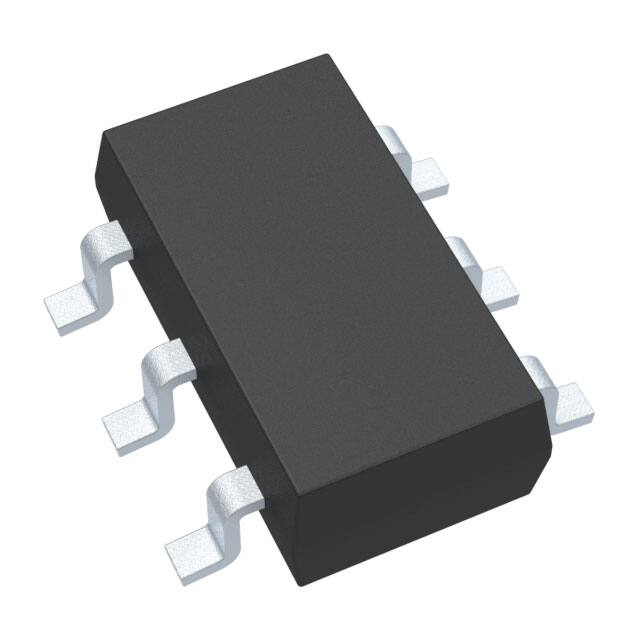
In Small SOT23-6 Package
POWER MANAGEMENT
Description
Features
The SC2603A is a versatile, low-cost, voltage-mode PWM
controller designed for DC/DC power supply applications.
A simple, fixed-voltage boost regulator can be implemented
using the SC2603A with a minimum of external components. The small device footprint allows for compact circuit
design.
Low cost / small size
Input voltage range: 5V to 30V
200kHz switching frequency
Up to 95% efficiency
1% reference voltage accuracy
Typical 800mA PWM gate drive capability
Internal compensation
Over current protection
SOT23-6 package is fully WEEE and RoHS compliant
SC2603A features include a temperature compensated
voltage reference, triangle wave oscillator, current limit
comparator, frequency shift over-current protection, and
an internally compensated error amplifier. Pulse by pulse
current limiting is implemented by sensing the differential
voltage across an external resistor, or an appropriately
sized PC board trace.
Applications
Portable Devices
Flat Panel TV
TV Set Top Box
Auxiliary Supplies
Peripheral Card Supplies
Industrial Power Supply
High Density DC/DC Conversion
The SC2603A operates at a fixed frequency of 200kHz,
providing an optimum compromise between efficiency,
external component size, and cost.
Typical Application Circuit
L1
VIN
1
R1
C3
+
D1
C1
+
Enable
5
3
C4
C2
Q1
D2
Optional
VOUT
2
1
R2
U1
VIN
EN/SS
FB
GATE
CS
GND
4
R5
6
2
C5
R6
R4
SC2603A
Figure 1: 12V to 25V/1A Boost Conveter
Revision: May 8, 2007
�
www.semtech.com
�SC2603A
POWER MANAGEMENT
Absolute Maximum Rating
Exceeding the specifications below may result in permanent damage to the device, or device malfunction. Operation outside of the parameters specified
in the Electrical Characteristics section is not implied. Exposure to Absolute Maximum rated conditions for extended periods of time may affect device
reliability.
Parameter
Symbol
Maximum
Units
VIN to GND
-0.3 to 20
V
GATE Pin Voltage
VGATE
-0.3 to 20
V
EN/SS Pin Voltage
VEN/SS
-0.3 to 7
V
FB Pin Voltage
VFB
-0.3 to 7
V
Thermal Resistance Junction to Ambient(1)
θ JA
165
°C/W
Thermal Resistance Junction to Case
θ JC
102
°C/W
TJ
150
°C
Storage Temperature Range
TSTG
-45 to +150
°C
Lead Temperature (Soldering)10 sec
TLEAD
300
°C
ESD Rating (Human Body Model)
ESD
2
kV
Input Voltage
Maximum Junction Temperature
Note:
(1) Mounting pad has to be larger than one square inch on two sided printed circuit board with minimum 1 ounce copper
Electrical Characteristics
Unless specified: VIN = 12V, VO = 25V; TA = TJ = -40°C to 125°C
Parameter
Symbols
Conditions
Min
Typ
Max
Units
16
V
4.5
V
General
VIN Supply Voltage
VIN
VIN UVLO Threshold
VUVLO
VIN UVLO Hysteresis
VHYS
VIN Supply Current
VIN Shutdown Current
4.5
VIN ramping up
4.2
400
mV
Current into VIN pin during switching
6.0
9.0
mA
EN/SS=Low
5.0
6.0
mA
1.250
1.275
V
2.0
8.0
µA
Error Amplifier
Reference Voltage
VFB
Feedback Bias Current
IFB
1.225
VIN = 12V, VFB = VEN/SS
Error Amplifier Gain(1)
105
V/V
Oscillator
Oscillator Frequency
TA = 25 °C
Oscillator Frequency Shift
190
VFB < VREF /2
Maximum Duty Cycle
90
200
210
kHz
50
kHz
95
%
Internal Ramp Peak
VR_PEAK
1.4
V
Internal Ramp Valley
VR_VALLEY
0.4
V
2007 Semtech Corp.
�
www.semtech.com
�SC2603A
POWER MANAGEMENT
Electrical Characteristics (Cont.)
Parameter
Symbols
Conditions
Min
Typ
Max
Units
Regulation
Load Regulation
IO = 0.1A to 1A
0.3
0.5
%
Line Regulation
VIN = 5V to 15V, Io = 0.1A
0.5
1.0
%
PWM Gate Drive
GATE Source Current
VIN = 12V, CGATE = 10nF
0.5
0.8
1.1
A
GATE Sink Current
VIN = 12V, CGATE = 10nF
0.5
0.8
1.1
A
Enable and Soft Start
Soft Start Charge Current
Enable/Soft Start Threshold
ISS
60
µA
V
Pull down below this level to
disable PWM Switch gate
0.09
0.12
CS
65
73
Switch Current Limit
Current Limit Threshold
80
mV
Note:
(1) Guaranteed by design
2007 Semtech Corp.
�
www.semtech.com
�SC2603A
POWER MANAGEMENT
Ordering Information
Pin Configurations
Part Number
Package
SC2603ASKTRT(1,2)
SOT23-6
SC2603AEVB
Evaluation Board
TOP VIEW
FB
1 6
CS
GND
2 5
VIN
EN/SS
3 4
GATE
Notes:
(1) Only available in tape and reel packaging. A reel
contains 3000 devices.
(2) Lead free product. This product is fully WEEE
and RoHS compliant.
(6 Pin SOT-23)
Pin Descriptions
Pin
Pin Name
Pin Function
1
FB
2
GND
3
EN/SS
Enable / Soft Start Pin
4
GATE
PWM gate driver output
5
VIN
Device input voltage
6
CS
Current Sense input
Error amplifier inverted input
Device ground
Block Diagram
OSCILLATOR
VIN
S
PWM
FB
R
GATE
Q
GND
25K
Current
Limit
CS
EN/SS
UV
VIN
1.25V
REF
1.25V
REF
70mV
UVLO
Figure 2: SC2603A Function Diagram
2007 Semtech Corp.
�
www.semtech.com
�SC2603A
POWER MANAGEMENT
Applications Information
Theory of Operation
Maximum Duty Cycle
The SC2603A is a versatile, low-cost, voltage-mode PWM
controller designed for DC/DC power supply applications.
In normal condition, the SC2603A operates at a fixed
200kHz. One exception is that when the FB pin voltage
drops to one half, the frequency will be shifted to one
fourth of 200kHz.
The maximum duty cycle, Dmax defines the upper limit of
power conversion ratio
VOUT
�
=
VIN
� − D MAX
SC2603A features include a temperature compensated
voltage reference, triangle wave oscillator, current limit
comparator, frequency shift over-current protection, and
an internally compensated error amplifier. Pulse by pulse
current limiting is implemented by sensing the differential
voltage across an external resistor, or an appropriately
sized PC board trace.
Clamping Diode D2 at Vin Pin
Since the Vin pin of the SC2603A is rated at 20V, when
the supply voltage is higher than 16V, a Zener diode D2
is required to limit the SC2603A supply voltage, as shown
in Fig.1. The clamping voltage of D2 has to be not higher
than 15V.
Setting the Output Voltage
Over Current Protection (OCP)
As shown in Fig.1, an external resistive divider R2 and R4
with its center tap tied to the FB pin sets the output voltage.
The over-current protection is implemented by a sensing
resistor and an internal current-limit comparator with a
threshold of 70mV. In each switching cycle, if the switching
current through the sensing resistor causing the voltage at
the CS pin reaches 70mV, the SC2603A will immediately
turn the gate pulse off to limit the current through the
power switch.
V
R 2 = R 4 OUT − �
�
.
25
V
Soft-Start
The figure below shows the current waveforms run into
over-current protection. At t1, the input current Iin begins
to increase as the load Iout builds up until it hits the OCP
threshold at t2. At t2, Vout begins to drop as Iout starts
increasing toward t3 while Vin and Iin remain the same.
At t3, there two events are happening. 1) Vout is at half of
its regulating voltage. At this point, the internal oscillator
runs into frequency shift mode and shifts the frequency to
one fourth of the operating frequency. 2) The diode starts
conducting current without limit causing Vin to fall due to
supply current limit. Finally, Vin and Vout both drops to zero
and Iin becomes the input supply current limit.
Soft-start prevents a DC-DC converter from drawing excessive current from the power source during start up. If the
soft-start time is made sufficiently long, then the output will
enter regulation without overshoot. An external capacitor
is connected from the EN/SS pin to the ground. After the
part’s input voltage surpasses the UVLO, the EN/SS pin is
allowed to charge its capacitor with 60µA. When 100mV
is reached at the EN/SS pin, the internal comp node is at
0.4V. The SC2603A will start switching, and the converter
output comes into regulation. Because the FB pin voltage
follows EN/SS pin voltage, finally, the EN/SS pin voltage will
be clamped at 1.25V same as the reference voltage.
A RC filter at the CS pin is necessary to filter out noise to
ensure accurate sensing.
Under Voltage Lockout
The value of the sensing resistor can be calculated by the
following equation:
The under voltage lockout circuit of the SC2603A assures
that the Gate output remains in the off state whenever the
supply voltage drops below set parameters. Lockout occurs
if Vin falls below 3.8V. Normal operation resumes once Vin
rises above 4.2V.
2007 Semtech Corp.
Rs = 70mV/Ipeak
�
www.semtech.com
�SC2603A
POWER MANAGEMENT
Applications Information (Cont.)
in more reliable gate switching signals.
where Ipeak is the input peak current through the power
MOSFET.
Normal
Loading
SS
3) The connection between the junction of Q1, D1 and the
output capacitor should be a wide trace or copper region.
It should be as short as practical. Since this connection
has fast voltage transitions, keeping this connection short
will minimize EMI.
Supply Current Limiting
OCP
4) The Output Capacitor(s) (Cout) should be located as
close to the load as possible, fast transient load currents
are supplied by Cout only, and connections between Cout
and the load must be short, wide copper areas to minimize
inductance and resistance.
IIN
IOUT
Layout Guidelines
5) The SC2603A is best placed over an isolated ground
plane area. The soft-start capacitor, the Vin decoupling capacitor, and the current sensing filter capacitor should also
connected to this ground pad area. This isolated ground
area should be connected to the main ground by a trace
that runs from the GND pin to the ground side of the output
capacitor. If this is not possible, the GND pin may be connected to the ground path between the Output Capacitor
and the Cin, Q1, D1 loop. Under no circumstances should
GND be returned to a ground inside the Cin, Q1, D1 loop.
Careful attentions to layout requirements are necessary
for successful implementation of the SC2603A PWM controller. High currents switching at 200kHz are present in
the application and their effect on ground plane voltage
differentials must be understood and minimized.
6) Input voltage of the SC2603A should be supplied from
the power rail through a 2.2~10Ω resistor, the Vin pin
should be decoupled directly to GND by a 0.1µF~1µF
ceramic capacitor, trace lengths should be as short as
possible.
1) The high power parts of the circuit should be laid out
first. A ground plane should be used. The number and
position of ground plane interruptions should be such as
to not unnecessarily compromise ground plane integrity.
Isolated or semi-isolated areas of the ground plane may
be deliberately introduced to constrain ground currents to
particular areas, for example the input capacitor and bottom Schottky ground.
7) An RC low pass filter is required to filter out leading
edge current spikes on the current sensing resistor. The
filter capacitor needs to be very close to the CS and GND
to reduce noise pickup.
VOUT
VIN
t0
t1
t2
t3
t4
Figure 3. Current Waveforms
2) The loop formed by the output Capacitor(s) (Cout), the
FET (Q1), the current sensing resistor, and the Schottky (D1)
must be kept as small as possible, as shown on the layout
diagram in Fig.4. This loop contains all the high current, fast
transition switching. Connections should be as wide and
as short as possible to minimize loop inductance. Minimizing this loop area will reduce EMI, lower ground injection
currents, resulting in electrically “cleaner” grounds for the
rest of the system and minimize source ringing, resulting
2007 Semtech Corp.
�
www.semtech.com
�SC2603A
POWER MANAGEMENT
Applications Information (Cont.)
Layout diagram for the SC2603A
Vout
12VIN
Ra
L1
D1
Cin
2.2
5
3
0.1uF
Q1
SC2603A
0.1uF
6
VIN
FB
EN/SS
GATE
CS
GND
Rb
1
+
Cout
4
Rs
2
Note: Heavy lines indicate the critical loop carrying high pulsating current.
The inductance of the loop needs to be minimized.
Figure 4: SC2603A Layout Diagram
2007 Semtech Corp.
�
www.semtech.com
�SC2603A
POWER MANAGEMENT
Applications Information (Cont.)
Typical application schematic with 12V input and 24V/1A output
12V INPUT
1
+
C1
220uF
D1
L1
C11
1uF
CMSH2-40M
33uH
C10
1uF
24V/1A OUTPUT
2
R1
2R2
Q1
IRF7821
R2
226k
+
C2
330uF
Rc
2.3k
U1
1
Cc
2
3
56nF
FB
CS
GND
VIN
EN/SS
C4
0.1uF
GATE
SC2603A
R5
6
R4
12.4k
1k
5
4
C3
1uF
C5
120pF
R6
20m
Bill of materials
Item Quantity Reference
1
1
C1
2
1
C2
3
2
C3,C10
4
1
C4
5
1
C5
6
1
C11
7
1
Cc
8
1
D1
9
1
L1
10
1
Q1
11
1
R1
12
1
R2
13
1
R4
14
1
R5
15
1
R6
16
1
Rc
17
1
U1
2007 Semtech Corp.
Part
220uF/16V
330uF/35V
1uF/16V
0.1uF
120pF
1uF/50V
56nF
CMSH2-40M
33uH/5.1A (HC8-330)
IRF7821
2R2
226k
12.4k
1k
20m
2.3k
SC2603A
Vendor
Panasonic
Nichicon, VR
Vishay
Vishay
Vishay
Vishay
Vishay
Central Semi
Coiltronics
IR
Vishay
Vishay
Vishay
Vishay
Vishay
Vishay
Semtech
�
www.semtech.com
�SC2603A
POWER MANAGEMENT
Outline Drawing - SOT23-6
DIM
A
e1
2X E/2
ccc C
2X N/2 TIPS
A
A1
A2
D
N
EI
1
b
c
D
E1
E
e
e1
L
L1
N
01
aaa
bbb
ccc
E
2
e
B
D
aaa C
SEATING
PLANE
A2
DIMENSIONS
INCHES
MILLIMETERS
MIN NOM MAX MIN NOM MAX
.057
.035
.000
.006
.035 .045 .051
.010
.020
.003
.009
.110 .114 .122
.060 .063 .069
.110 BSC
.037 BSC
.075 BSC
.012 .018 .024
(.024)
bxN
bbb
10°
0°
6
0.10
0.20
0.20
10°
A
H
A1
C
6
.004
.008
.008
0°
1.45
0.90
0.00
0.15
.90 1.15 1.30
0.25
0.50
0.08
0.22
2.80 2.90 3.10
1.50 1.60 1.75
2.80 BSC
0.95 BSC
1.90 BSC
0.30 0.45 0.60
(0.60)
C A-B D
c
GAGE
PLANE
0.25
L
(L1)
SEE DETAIL
A
DETAIL
01
A
SIDE VIEW
NOTES:
1.
CONTROLLING DIMENSIONS ARE IN MILLIMETERS (ANGLES IN DEGREES).
2.
DATUMS -A- AND -B- TO BE DETERMINED AT DATUM PLANE -H-
3.
DIMENSIONS "E1" AND "D" DO NOT INCLUDE MOLD FLASH, PROTRUSIONS
OR GATE BURRS.
Land Pattern - SOT23-6
X
DIM
(C)
G
Z
Y
P
C
G
P
X
Y
Z
DIMENSIONS
INCHES
MILLIMETERS
(.098)
.055
.037
.024
.043
.141
(2.50)
1.40
0.95
0.60
1.10
3.60
NOTES:
1.
THIS LAND PATTERN IS FOR REFERENCE PURPOSES ONLY.
CONSULT YOUR MANUFACTURING GROUP TO ENSURE YOUR
COMPANY'S MANUFACTURING GUIDELINES ARE MET.
Contact Information
Semtech Corporation
Power Management Products Division
200 Flynn Road, Camarillo, CA 93012
Phone: (805)498-2111 FAX (805)498-3804
2007 Semtech Corp.
�
www.semtech.com
�


 工商网监
湘ICP备2023018690号
工商网监
湘ICP备2023018690号
