Thyristors
Surface Mount – 50 - 800V > 2N6400
2N6400
Pb
Description
Designed primarily for half-wave ac control applications,
such as motor controls, heating controls and power
supplies; or wherever half−wave silicon gate−controlled,
solid−state devices are needed.
Features
• Glass Passivated Junctions for Greater Parameter
Uniformity and Stability
• Small, Rugged, Thermowatt Construction for Low Thermal
Resistance, High Heat Dissipation and Durability
• Blocking Voltage to 800 V
• These are Pb−Free devices
Pin Out
Functional Diagram
4
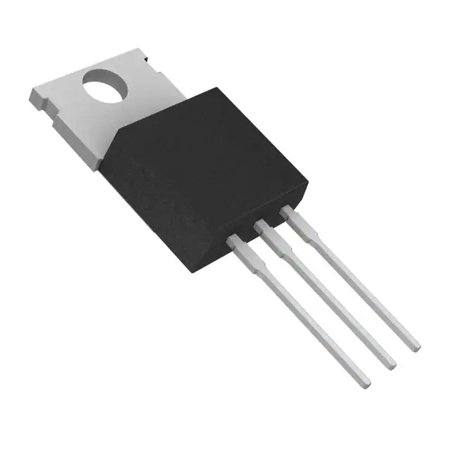
TO 220AB
CASE 221A
STYLE 3
1
2
2N640xG
AYWW
Additional Information
3
Datasheet
Resources
Samples
© 2017 Littelfuse, Inc.
Specifications are subject to change without notice.
Revised: 09/15/17
�Thyristors
Surface Mount – 50 - 800V > 2N6400
Maximum Ratings † (TJ = 25°C unless otherwise noted)
Rating
Peak Repetitive Off-State Voltage (Note 1)
(TJ = -40 to 110°C, Sine Wave, 50 to 60 Hz, Gate Open)
Part Number
Symbol
Value
2N6400
50
2N6401
100
2N6402
VDRM,
200
2N6403
VRRM
400
2N6404
600
2N6405
800
On-State RMS Current
IT
Unit
V
(RMS)
16
A
(AV)
10
A
ITSM
160
A
I2t
145
A2s
Forward Peak Gate Power (Pulse Width ≤ 1.0 µs, TC = 100°C)
PGM
20
W
Forward Average Gate Power (t = 8.3 ms, TC = 100°C)
PG(AV)
0.5
W
Forward Peak Gate Current (Pulse Width ≤ 1.0 µs, TC = 100°C)
IGM
2.0
A
Operating Junction Temperature Range
TJ
-40 to +125
°C
Storage Temperature Range
Tstg
-40 to +125
°C
(180° Conduction Angles; TC = 100°C)
Average On-State RMS Current
IT
(180° Conduction Angles; TC = 100°C)
Peak Non−Repetitive Surge Current
(1/2 Cycle, Sine Wave, 60 Hz, TJ = 90°C)
Circuit Fusing Considerations (t = 8.3 ms)
†Indicates JEDEC Registered Data
Stresses exceeding Maximum Ratings may damage the device. Maximum Ratings are stress ratings only. Functional operation above the Recommended Operating Conditions is
not implied. Extended exposure to stresses above the Recommended Operating Conditions may affect device reliability.
1. VDRM and VRRM for all types can be applied on a continuous basis. Ratings apply for zero or negative gate voltage; however, positive gate voltage shall not be applied concurrent
with negative potential on the anode. Blocking voltages shall not be tested with a constant current source such that the voltage ratings of the devices are exceeded.
Maximum Ratings † (TJ = 25°C unless otherwise noted)
Rating
Thermal Resistance, Junction-to-Case
Maximum Lead Temperature for Soldering Purposes, 1/8” from
case for 10 seconds
Symbol
Value
Unit
RΘJC
1.5
°C/W
TL
260
°C
† Indicates JEDEC Registered Data
© 2017 Littelfuse, Inc.
Specifications are subject to change without notice.
Revised: 09/15/17
�Thyristors
Surface Mount – 50 - 800V > 2N6400
Electrical Characteristics - OFF (TC = 25°C unless otherwise noted)
Characteristic
TJ = 25°C
†Peak Repetitive Blocking Current
(VAK = VDRM = VRRM; Gate Open)
TJ = 125°C
Symbol
Min
Typ
Max
Unit
IDRM,
-
-
1.0
µA
-
-
2.0
mA
IRRM
Electrical Characteristics - ON
Characteristic
Symbol
Min
Typ
Max
Unit
VTM
−
–
1.7
V
−
9.0
30
−
−
60
−
0.7
1.5
−
−
2.5
0.2
−
−
−
18
40
−
−
60
−
1.0
–
−
15
−
−
35
−
†Peak Forward On−State Voltage
(ITM = 32 A Peak, Pulse Width ≤ 1 ms, Duty Cycle ≤ 2%)
TC = 25°C
†Gate Trigger Voltage (Continuous DC), All Quadrants
(Continuous dc) (VD = 12 Vdc, RL = 100 Ω)
IGT
TC= -40°C
TC = 25°C
†Gate Trigger Voltage (Continuous dc) (VD = 12 Vdc, RL = 100 Ω)
VGT
TC= -40°C
TC = +125°C
Gate Non−Trigger Voltage (VD = 12 Vdc, RL = 100 Ω)
†Holding Current (VD = 12 Vdc, Initiating Current = 200 mA, Gate Open)
VGD
TC = 25°C
IH
TC= -40°C
Turn-On Time (ITM = 12 A, IGT = 40 mAdc, VD = Rated VDRM)
tgt
TC = 25°C
Turn-Off Time (ITM = 16 A, IR = 16 A, VD = Rated VDRM)
tq
TJ= +125°C
mA
V
V
mA
µs
µs
†Indicates JEDEC Registered Data
Dynamic Characteristics
Characteristic
Critical Rate−of−Rise of Off-State Voltage
(VD = Rated VDRM, Exponential Waveform)
TJ= +125°C
Symbol
Min
Typ
Max
Unit
dv/dt(c)
−
50
−
V/µs
© 2017 Littelfuse, Inc.
Specifications are subject to change without notice.
Revised: 09/15/17
�Thyristors
Surface Mount – 50 - 800V > 2N6400
Voltage Current Characteristic of SCR
Symbol
Parameter
VDRM
Peak Repetitive Forward Off State Voltage
IDRM
Peak Forward Blocking Current
VRRM
Peak Repetitive Reverse Off State Voltage
IRRM
Peak Reverse Blocking Current
VTM
Maximum On State Voltage
IH
I
I
I
Holding Current
Figure 1. Current Derating
Figure 2. Maximum On-State Power Dissipation
°
TJ ≈
α
°C
°
α = CONDUCTION ANGLE
°
°
α
°
dc
α
°
°
°
°
α
α = CONDUCTION ANGLE
°
7.0
IT(AV)
© 2017 Littelfuse, Inc.
Specifications are subject to change without notice.
Revised: 09/15/17
�Thyristors
Surface Mount – 50 - 800V > 2N6400
Figure 3. On−State Characteristics
Figure 4. Maximum Non−Repetitive Surge Current
r(t), TRANSIENT THERMAL RESISTANCE (NORMALIZED)
Figure 5. Thermal Response
© 2017 Littelfuse, Inc.
Specifications are subject to change without notice.
Revised: 09/15/17
�Thyristors
Surface Mount – 50 - 800V > 2N6400
Typical Characteristics
Figure 6. Typical Gate Trigger Current vs. Pulse Width
Figure 7. Typical Gate Trigger Current vs. Junction Temperature
Figure 8. Typical Gate Trigger Voltage vs. Junction Temperature
Figure 9. Typical Holding Current vs. Junction Temperature
© 2017 Littelfuse, Inc.
Specifications are subject to change without notice.
Revised: 09/15/17
�Thyristors
Surface Mount – 50 - 800V > 2N6400
Dimensions
Part Marking System
SEATING
PLANE
B
F
4
Q
12
4
C
T
S
TO 220AB
CASE 221A
STYLE 3
A
U
3
H
1
K
Z
2
R
L
V
D
N
Inches
Millimeters
3
x=
A=
Y=
WW
G=
J
G
Dim
2N640xG
AYWW
0, 1, 2, 3, 4 or 5
Assembly Location
Year
= Work Week
Pb Free Package
Pin Assignment
Min
Max
Min
Max
1
Cathode
A
0.570
0.620
14.48
15.75
2
Anode
B
0.380
0.405
9.66
10.28
3
Gate
C
0.160
0.190
4.07
4.82
D
0.025
0.035
0.64
0.88
4
Anode
F
0.142
0.147
3.61
3.73
G
0.095
0.105
2.42
2.66
H
0.110
0.155
2.80
3.93
J
0.014
0.022
0.36
0.55
K
0.500
0.562
12.70
14.27
L
0.045
0.060
1.15
1.52
N
0.190
0.210
4.83
5.33
Q
0.100
0.120
2.54
3.04
R
0.080
0.110
2.04
2.79
S
0.045
0.055
1.15
1.39
T
0.235
0.255
5.97
6.47
U
0.000
0.050
0.00
1.27
V
0.045
−−−
1.15
−−−
Z
−−−
0.080
−−−
2.04
1. DIMENSIONING AND TOLERANCING PER ANSI Y14.5M, 1982.
Ordering Information
Device
Package
Shipping
2N6400G
2N6401G
500 Units / Box
2N6402G
2N6403G
2N6403TG
TO-220AB
(Pb-Free)
50 Units / Rail
2N6404G
500 Units / Box
2N6405G
2. CONTROLLING DIMENSION: INCH.
3. DIMENSION Z DEFINES A ZONE WHERE ALL BODY AND
LEAD IRREGULARITIES ARE ALLOWED.
Disclaimer Notice - Information furnished is believed to be accurate and reliable. However, users should independently evaluate the suitability of and
test each product selected for their own applications. Littelfuse products are not designed for, and may not be used in, all applications. Read complete
Disclaimer Notice at: www.littelfuse.com/disclaimer-electronics.
© 2017 Littelfuse, Inc.
Specifications are subject to change without notice.
Revised: 09/15/17
�


 工商网监
湘ICP备2023018690号
工商网监
湘ICP备2023018690号
