IXD_630
30-Ampere Low-Side
Ultrafast MOSFET Drivers
INTEGRATED CIRCUITS DIVISION
Features
Description
• 30A Peak Source/Sink Drive Current
• High Operating Voltage Capability: 35V
• -40°C to +125°C Extended Operating Temperature
Range
• Under-Voltage Lockout Protection
• Logic Input Withstands Negative Swing of up to 5V
• Fast Rise and Fall Times: < 20ns
• Low Propagation Delay Time
• Low 10A Supply Current
• Low Output Impedance
The IXDD630/IXDI630/IXDN630 high-speed gate
drivers are especially well suited for driving the latest
IXYS power MOSFETs and IGBTs. The IXD_630
output can source and sink 30A of peak current while
producing voltage rise and fall times of less than 20ns.
Internal circuitry eliminates cross conduction and
current "shoot-through," and the driver is virtually
immune to latch up. Under-voltage lockout (UVLO)
circuitry holds the output LOW until sufficient supply
voltage is applied (12.5V for the IXD_630 versions,
and 9V for the IXD_630M versions). Low propagation
delays and fast, matched rise and fall times make the
IXD_630 family ideal for very high frequency and
high-power applications.
Applications
•
•
•
•
•
•
Efficient Power MOSFET and IGBT Switching
Switch Mode Power Supplies
Motor Controls
DC to DC Converters
Class-D Switching Amplifiers
Pulse Transformer Driver
The IXDD630 is configured as a non-inverting driver
with an enable. The IXDN630 is configured as a
non-inverting driver, and the IXDI630 is configured as
an inverting driver.
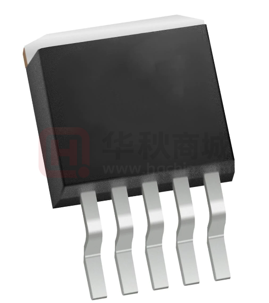
The IXD_630 family is available in a 5-pin TO-220 (CI),
and a 5-pin TO-263 (YI) package.
Ordering Information
Part Number
IXDD630CI
IXDD630MCI
IXDD630YI
IXDD630MYI
IXDI630CI
IXDI630MCI
IXDI630YI
IXDI630MYI
IXDN630CI
IXDN630MCI
IXDN630YI
IXDN630MYI
DS-IXD_630-R04
Logic
Configuration
IN
OUT
EN
IN
OUT
IN
OUT
UVLO
Package Type
Packing
Method
Quantity
12.5V
9V
12.5V
9V
12.5V
9V
12.5V
9V
12.5V
9V
12.5V
9V
5-Pin TO-220
5-Pin TO-220
5-Pin TO-263
5-Pin TO-263
5-Pin TO-220
5-Pin TO-220
5-Pin TO-263
5-Pin TO-263
5-Pin TO-220
5-Pin TO-220
5-Pin TO-263
5-Pin TO-263
Tube
Tube
Tube
Tube
Tube
Tube
Tube
Tube
Tube
Tube
Tube
Tube
50
50
50
50
50
50
50
50
50
50
50
50
www.ixysic.com
1
�IXD_630
INTEGRATED CIRCUITS DIVISION
1. Specifications . . . . . . . . . . . . . . . . . . . . . . . . . . . . . . . . . . . . . . . . . . . . . . . . . . . . . . . . . . . . . . . . . . . . . . . . . . . . . . . . . . . . . . . . . . . . . .
1.1 Lead Configurations. . . . . . . . . . . . . . . . . . . . . . . . . . . . . . . . . . . . . . . . . . . . . . . . . . . . . . . . . . . . . . . . . . . . . . . . . . . . . . . . . . . . . .
1.2 Lead Definitions . . . . . . . . . . . . . . . . . . . . . . . . . . . . . . . . . . . . . . . . . . . . . . . . . . . . . . . . . . . . . . . . . . . . . . . . . . . . . . . . . . . . . . . . .
1.3 Absolute Maximum Ratings . . . . . . . . . . . . . . . . . . . . . . . . . . . . . . . . . . . . . . . . . . . . . . . . . . . . . . . . . . . . . . . . . . . . . . . . . . . . . . . .
1.4 Recommended Operating Conditions . . . . . . . . . . . . . . . . . . . . . . . . . . . . . . . . . . . . . . . . . . . . . . . . . . . . . . . . . . . . . . . . . . . . . . . .
1.5 Electrical Characteristics: TA = 25°C . . . . . . . . . . . . . . . . . . . . . . . . . . . . . . . . . . . . . . . . . . . . . . . . . . . . . . . . . . . . . . . . . . . . . . . . .
1.6 Electrical Characteristics: TA = - 40°C to +125°C . . . . . . . . . . . . . . . . . . . . . . . . . . . . . . . . . . . . . . . . . . . . . . . . . . . . . . . . . . . . . . .
1.7 Thermal Characteristics . . . . . . . . . . . . . . . . . . . . . . . . . . . . . . . . . . . . . . . . . . . . . . . . . . . . . . . . . . . . . . . . . . . . . . . . . . . . . . . . . . .
3
3
3
3
4
4
5
5
2. Functional Description . . . . . . . . . . . . . . . . . . . . . . . . . . . . . . . . . . . . . . . . . . . . . . . . . . . . . . . . . . . . . . . . . . . . . . . . . . . . . . . . . . . . . . .
2.1 IXDD630 Block Diagram & Truth Table . . . . . . . . . . . . . . . . . . . . . . . . . . . . . . . . . . . . . . . . . . . . . . . . . . . . . . . . . . . . . . . . . . . . . . .
2.2 IXDI630 Block Diagram & Truth Table. . . . . . . . . . . . . . . . . . . . . . . . . . . . . . . . . . . . . . . . . . . . . . . . . . . . . . . . . . . . . . . . . . . . . . . .
2.3 IXDN630 Block Diagram & Truth Table . . . . . . . . . . . . . . . . . . . . . . . . . . . . . . . . . . . . . . . . . . . . . . . . . . . . . . . . . . . . . . . . . . . . . . .
6
6
6
6
3. Typical Performance Characteristics . . . . . . . . . . . . . . . . . . . . . . . . . . . . . . . . . . . . . . . . . . . . . . . . . . . . . . . . . . . . . . . . . . . . . . . . . . . 7
4. Manufacturing Information . . . . . . . . . . . . . . . . . . . . . . . . . . . . . . . . . . . . . . . . . . . . . . . . . . . . . . . . . . . . . . . . . . . . . . . . . . . . . . . . . . .
4.1 Moisture Sensitivity . . . . . . . . . . . . . . . . . . . . . . . . . . . . . . . . . . . . . . . . . . . . . . . . . . . . . . . . . . . . . . . . . . . . . . . . . . . . . . . . . . . . .
4.2 ESD Sensitivity . . . . . . . . . . . . . . . . . . . . . . . . . . . . . . . . . . . . . . . . . . . . . . . . . . . . . . . . . . . . . . . . . . . . . . . . . . . . . . . . . . . . . . . .
4.3 Reflow Profile. . . . . . . . . . . . . . . . . . . . . . . . . . . . . . . . . . . . . . . . . . . . . . . . . . . . . . . . . . . . . . . . . . . . . . . . . . . . . . . . . . . . . . . . . .
4.4 Board Wash . . . . . . . . . . . . . . . . . . . . . . . . . . . . . . . . . . . . . . . . . . . . . . . . . . . . . . . . . . . . . . . . . . . . . . . . . . . . . . . . . . . . . . . . . . .
4.5 Mechanical Dimensions. . . . . . . . . . . . . . . . . . . . . . . . . . . . . . . . . . . . . . . . . . . . . . . . . . . . . . . . . . . . . . . . . . . . . . . . . . . . . . . . . .
2
www.ixysic.com
10
10
10
10
10
11
R04
�IXD_630
INTEGRATED CIRCUITS DIVISION
1 Specifications
1.1 Lead Configurations
1.2 Lead Definitions
IXDD630 CI / YI
Lead Name
VCC
1
OUT
2
GND
3
IN
4
EN
5
IN
Logic Input
EN
Output Enable - Drive lead low to disable
output, and force output to a high impedance
state
OUT
Output - Sources or sinks current to turn-on or
turn-off a discrete MOSFET or IGBT
OUT
Inverted Output - Sources or sinks current to
turn-on or turn-off a discrete MOSFET or IGBT
VCC
Supply Voltage - Provides power to the device
GND
Ground - Common ground reference for the
device
IXDI630 CI / YI
VCC
1
OUT
2
GND
3
IN
4
NC
5
Description
NC
Not connected
IXDN630 CI / YI
VCC
1
OUT
2
GND
3
IN
4
NC
5
1.3 Absolute Maximum Ratings
Parameter
Supply Voltage
Input Voltage Range
Output Current
Symbol
Minimum
Maximum
Units
VCC
-0.3
40
V
VIN , VEN
-5
VCC+0.3
V
IOUT
-
±30
A
Junction Temperature
TJ
-55
+150
°C
Storage Temperature
TSTG
-65
+150
°C
Unless stated otherwise, absolute maximum electrical ratings are at 25°C
Absolute maximum ratings are stress ratings. Stresses in excess of these ratings can cause permanent damage to the device.
Functional operation of the device at conditions beyond those indicated in the operational sections of this data sheet is not
implied.
R04
www.ixysic.com
3
�IXD_630
INTEGRATED CIRCUITS DIVISION
1.4 Recommended Operating Conditions
Parameter
Supply Voltage
Operating Temperature Range
Symbol
Range
Units
VCC
UVLO to 35
V
TA
-40 to +125
°C
1.5 Electrical Characteristics: TA = 25°C
Test Conditions: UVLO < VCC < 35V (unless otherwise noted).
Parameter
Conditions
Symbol
Minimum
Typical
Maximum
Input Voltage, High
UVLO < VCC < 18V
VIH
3.5
-
-
Input Voltage, Low
UVLO < VCC < 18V
VIL
-
-
0.8
Input Current
0V < VIN < VCC
IIN
-
-
±10
EN Input Voltage, High
IXDD630 only
VENH
2/3VCC
-
-
EN Input Voltage, Low
IXDD630 only
VENL
-
-
1/3VCC
Output Voltage, High
-
VOH
VCC-0.025
-
-
Output Voltage, Low
-
VOL
-
-
0.025
Output Resistance, High State
VCC=18V, IOUT= -100mA
ROH
-
0.17
0.4
Output Resistance, Low State
VCC=18V, IOUT=100mA
ROL
-
0.16
0.3
IDC
-
-
±8
tr
-
11
20
Units
V
A
V
V
Rise Time
Limited by package power
dissipation
CLOAD=5.6nF, VCC=18V
Fall Time
CLOAD=5.6nF, VCC=18V
tf
-
11
18
On-Time Propagation Delay
CLOAD=5.6nF, VCC=18V
tondly
-
46
65
Off-Time Propagation Delay
CLOAD=5.6nF, VCC=18V
toffdly
-
46
65
Output Enable Time
IXDD630 only
tPZL, tPZH
-
34
65
Output Disable Time
IXDD630 only
tPLZ, tPHZ
-
65
125
IXDD630 only
REN
-
400
-
k
-
2.5
4
mA
-
-
0.75
-
-
0.75
7
9
9.9
10
12.5
13.5
Output Current, Continuous
Enable Pull-Up Resistor
VCC=18V, VIN=3.5V
Power Supply Current
VCC=18V, VIN=0V
ICC
VCC=18V, VIN=VCC
Under-Voltage Lockout Threshold
Under-Voltage Lockout Hysteresis
4
VCC Rising, IXD_630M
VCC Rising, IXD_630
IXD_630M
IXD_630
www.ixysic.com
UVLO
-
-
1
-
-
1.5
-
A
ns
mA
V
V
R04
�IXD_630
INTEGRATED CIRCUITS DIVISION
1.6 Electrical Characteristics: TA = - 40°C to +125°C
Test Conditions: UVLO < VCC < 35V, TJ
很抱歉,暂时无法提供与“IXDD630YI”相匹配的价格&库存,您可以联系我们找货
免费人工找货- 国内价格 香港价格
- 1+101.553361+12.30939
- 10+93.4960710+11.33276
- 50+60.4264450+7.32435
- 100+56.28185100+6.82198
- 250+54.85071250+6.64851
- 500+51.19436500+6.20532
- 1000+45.599571000+5.52717
- 国内价格 香港价格
- 1+62.292811+7.56560
- 10+52.2307410+6.34354
- 50+46.2031950+5.61148


 工商网监
湘ICP备2023018690号
工商网监
湘ICP备2023018690号
