TVS Diode Arrays (SPA®® Diodes)
Enhanced ESD Discrete TVS Series - SP3522
SP3530
SP3522 0.15pF 22kV avalanche diodes
RoHS Pb GREEN ELV
Description
The SP3522 integrates ultra low capacitance cathode-tocathode silicon avalanche diodes to provide protection
for electronic equipment that may experience destructive
electrostatic discharges (ESD). This robust component can
safely absorb repetitive ESD strikes above the maximum
level specified in the IEC 61000-4-2 international standard
(±8kV contact discharge) without performance degradation.
The extremely low loading capacitance also makes it ideal
for protecting high speed signal pins such as V-By-One®,
HDMI, USB3.0, USB2.0, and IEEE 1394.
Pinout
Features
Bottom View
1
1
1
1
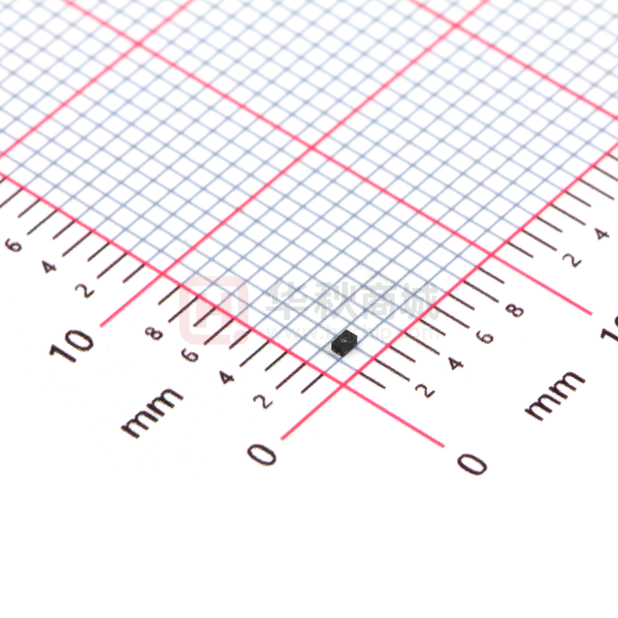
SOD882
2
2
2
2
0201 DFN Bottom View
Functional Block Diagram
1
1
SOD882
• ESD, IEC 61000-4-2,
±22kV contact, ±22kV air
• Facilitates excellent signal
integrity
• EFT, IEC 61000-4-4, 40A
(tP=5/50ns)
• ELV Compliant
• Lightning, IEC 610004-5, 2nd edition, 2.5A
(tP=8/20μs)
• Halogen free, Lead free
and RoHS compliant
• Low capacitance of
0.15pF (TYP) at 3GHz
Applications
• Ultra-high speed data
lines
• C
� onsumer, mobile and
portable electronics
• USB 3.1, 3.0, 2.0
• Tablet PC and external
storage with high speed
interfaces
• DisplayPort(TM)
Unidirectional
• V-by-One®
2
Bidirectional
©2017 Littelfuse, Inc.
Specifications are subject to change without notice.
Revision: 07/03/17
• Moisture Sensitivity Level
(MSL-1)
• Low profile 0201 DFN
packages and SOD882
packages
• HDMI 2.0, 1.4a, 1.3
2
• AEC-Q101 qualified
• LVDS interfaces
• Applications requiring
high ESD performance in
small packages
�TVS Diode Arrays (SPA®® Diodes)
Enhanced ESD Discrete TVS Series - SP3522
SP3530 Series
Absolute Maximum Ratings
Symbol
Parameter
Value
Units
IPP
Peak Current (tp=8/20μs)
2.5
A
TOP
Operating Temperature
-45 to 125
°C
TSTOR
Storage Temperature
-55 to 150
°C
CAUTION: Stresses above those listed in “Absolute Maximum Ratings” may cause
permanent damage to the component. This is a stress only rating and operation of the
component at these or any other conditions above those indicated in the operational
sections of this specification is not implied.
Electrical Characteristics - (TOP=25°C)
Parameter
Test Conditions
Min
Typ
Max
Units
Input Capacitance
@ VR = 0V, f = 3GHz
0.15
pF
Breakdown Voltage
VBR @ IT=1mA
9.2
V
Reverse Working Voltage
IR≤1μA
Reverse Leakage Current
IL @ VRWM=5.0V
0.02
TLP, tP=100ns, I/O to GND
0.96
Ω
14.5
V
Dynamic Resistance
2
VCL @ IPP=2.5A
Clamping Voltage
1
ESD Withstand Voltage1
IEC 61000-4-2 (Contact)
±22
IEC 61000-4-2 (Air)
±22
7.0
V
1
μA
kV
Note:
1. Parameter is guaranteed by design and/or component characterization.
2.Transmission Line Pulse (TLP) with 100ns width, 2ns rise time, and average window t1=70ns to t2= 90ns
Clamping Voltage vs IPP
8/20μs Pulse Waveform
110%
16.0
100%
90%
12.0
80%
10.0
Percent of IPP
Clamp Voltage (VC)
14.0
8.0
6.0
4.0
50%
40%
30%
2.0
20%
0.0
10%
1
1.5
2
Peak Pulse Current-IPP (A)
©2017 Littelfuse, Inc.
Specifications are subject to change without notice.
Revision: 07/03/17
70%
60%
2.5
0%
0.0
5.0
10.0
15.0
Time (μs)
20.0
25.0
30.0
�TVS Diode Arrays (SPA®® Diodes)
Enhanced ESD Discrete TVS Series - SP3522
SP3530
Positive Transmission Line Pulsing (TLP) Plot
Negative Transmission Line Pulsing (TLP) Plot
0
35
-5
30
-10
TLP Current (A)
TLP Current (A)
40
25
20
15
-15
-20
-25
10
-30
5
-35
0
-40
0
5
10
15
20
25
30
35
40
45
50
55
-55 -50 -45 -40 -35 -30 -25 -20 -15 -10
TLP Voltage (V)
TLP Voltage (V)
IEC 61000−4−2 +8 kV Contact ESD Clamping Voltage
-5
0
IEC 61000−4−2 -8 kV Contact ESD Clamping Voltage
Soldering Parameters
- Temperature Min (Ts(min))
Pre Heat
Pb – Free assembly
150°C
- Temperature Max (Ts(max))
200°C
- Time (min to max) (ts)
60 – 180 secs
Average ramp up rate (Liquidus) Temp (TL)
to peak
3°C/second max
TS(max) to TL - Ramp-up Rate
3°C/second max
Reflow
- Temperature (TL) (Liquidus)
217°C
- Temperature (tL)
60 – 150 seconds
Peak Temperature (TP)
260+0/-5 °C
Time within 5°C of actual peak
Temperature (tp)
20 – 40 seconds
Ramp-down Rate
6°C/second max
Time 25°C to peak Temperature (TP)
8 minutes Max.
Do not exceed
260°C
©2017 Littelfuse, Inc.
Specifications are subject to change without notice.
Revision: 07/03/17
tP
TP
Temperature
Reflow Condition
Critical Zone
TL to TP
Ramp-up
TL
TS(max)
tL
Ramp-do
Ramp-down
Preheat
TS(min)
25
tS
time to peak temperature
Time
�TVS Diode Arrays (SPA®® Diodes)
Enhanced ESD Discrete TVS Series - SP3522
SP3530
Package Dimensions — 0201 DFN
D
e
E
L2
Symbol
PIN1
L1
Top View
h
1
A1
A
Bottom View
Millimeters
Inches
Min
Max
Max
Min
Min
Max
A
0.23
0.28
0.33
0.009
0.011
0.013
A1
0.00
0.02
0.05
0.000
0.001
0.002
L1
0.12
0.18
0.24
0.005
0.007
0.009
L2
0.18
0.24
0.30
0.007
0.009
0.012
D
0.55
0.60
0.65
0.022
0.024
0.026
E
0.25
0.30
0.35
0.010
0.012
0.014
e
0.35 (BSC)
0.014 (BSC)
h
0.05 ( x 45° )
0.002 ( x 45° )
Millimeters
Inches
Side View
Side View
Package outline
0.32mm
0.14mm
0.24mm
Recommended soldering pad layout
Package Dimensions — SOD882
D
e
h
E
L2
Symbol
L1
PIN1
Top View
1
Bottom View
0.65mm
A
A1
Package outline
Side View
0.40mm
Recommended soldering pad layout
Part Numbering System
SP 3522 – 01 U T G
G= Green
T= Tape & Reel
Series
Number of
Channels
©2017 Littelfuse, Inc.
Specifications are subject to change without notice.
Revision: 07/03/17
Max
Max
Min
Min
Max
0.40
0.45
0.50
0.016
0.018
0.020
A1
0.00
0.02
0.05
0.000
0.001
0.002
L1
0.20
0.25
0.30
0.008
0.010
0.012
L2
0.45
0.50
0.55
0.018
0.020
0.022
D
0.90
1.00
1.10
0.035
0.039
0.043
E
0.50
0.60
0.70
0.020
0.024
0.028
e
0.65 (BSC)
0.026 (BSC)
h
0.125 ( x 45° )
0.005 ( x 45° )
0.30mm
1.10mm
TVS Diode Arrays
(SPA® Diodes)
Min
A
Package
U: 0201 DFN
E: SOD882
Part Marking System
+
Ordering Information
Part Number
Package
SP3522-01UTG
0201 DFN
SP3522-01ETG
SOD882
Marking
+
Min. Order Qty.
15000
10000
�TVS Diode Arrays (SPA®® Diodes)
Enhanced ESD Discrete TVS Series - SP3522
SP3530
Embossed Carrier Tape & Reel Specification — 0201 DFN
P1
Device Orientation in Tape
D0
P2
P0
Symbol
Millimeters
A0
0.33 min/0.41 max
E1
F
W
Pin1 Location
D1
T
A0
K0
B0
0.63 min/0.71 max
D0
ø 1.50 +0.10/ -0
D1
ø 0.20 +/- 0.05
E1
1.75+/-0.10
F
3.50+/-0.05
K0
0.30 min/0.39 max
P0
4.00+/-0.10
P1
2.00+/-0.10
P2
2.00+/-0.05
W
8.00+0.30/-0.10
T
0.13 min/0.25 max
B0
8mm TAPE AND REEL
Embossed Carrier Tape & Reel Specification — SOD882
Symbol
Millimeters
A0
0.70+/-0.045
B0
1.10+/-0.045
K0
0.65+/-0.045
F
3.50+/-0.05
P1
2.00+/-0.10
W
8.00 + 0.30 -0.10
Device Orientation in Tape
Pin1 Location
8mm TAPE AND REEL
Disclaimer Notice - Information furnished is believed to be accurate and reliable. However, users should independently evaluate the suitability of and
test each product selected for their own applications. Littelfuse products are not designed for, and may not be used in, all applications.
Read complete Disclaimer Notice at www.littelfuse.com/disclaimier-electronics.
©2017 Littelfuse, Inc.
Specifications are subject to change without notice.
Revision: 07/03/17
�
很抱歉,暂时无法提供与“SP3522-01ETG”相匹配的价格&库存,您可以联系我们找货
免费人工找货- 国内价格
- 10+0.45965
- 100+0.39053
- 300+0.35597
- 1000+0.33005
- 5000+0.30932
- 10000+0.29895


 工商网监
湘ICP备2023018690号
工商网监
湘ICP备2023018690号