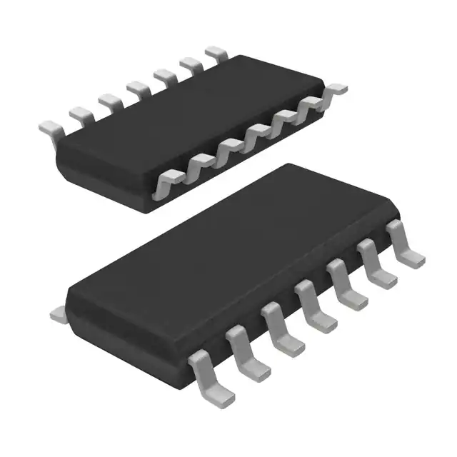
HD74LV74A
Dual D–type Flip Flops with Preset and Clear
ADE-205-244 (Z) 1st Edition March 1999 Description
The HD74LV74A has independent data, preset, clear, and clock inputs Q and Q outputs in a 14 pin package. The input data is transferred to the output at the rising edge of clock pulse CLK. Low-voltage and high-speed operation is suitable for the battery-powered products (e.g., notebook computers), and the low-power consumption extends the battery life.
Features
• • • • • • VCC = 2.0 V to 5.5 V operation All inputs VIH (Max.) = 5.5 V (@VCC = 0 V to 5.5 V) All outputs VO (Max.) = 5.5 V (@VCC = 0 V) Typical VOL ground bounce < 0.8 V (@VCC = 3.3 V, Ta = 25°C) Typical VOH undershoot > 2.3 V (@VCC = 3.3 V, Ta = 25°C) Output current ±6 mA (@VCC = 3.0 V to 3.6 V), ±12 mA (@VCC = 4.5 V to 5.5 V)
�HD74LV74A
Function Table
Inputs PRE L H L H H H CLR H L L H H H CLK X X X ↑ ↑ ↓ D X X X H L X Outputs Q H L H* H L Q0
1
Q L H H*1 L H Q0
Note: H: High level L: Low level X: Immaterial ↑: Low to high transition ↓: High to low transition Q0:The level of Q immediately before the input conditions shown in the above table are determined. 1.: Q and Q will remain HIGH as long as Preset and Clear are Low, but Q and Q are unpredictable, if Preset and Clear go HIGH simultaneously.
Pin Arrangement
1CLR 1 1D 1CLK 2 3
14 VCC 13 2CLR 12 2D 11 2CLK 10 2PRE 9 2Q 8 2Q
1PRE 4 1Q 1Q 5 6
GND 7
(Top view)
2
�HD74LV74A
Absolute Maximum Ratings
Item Supply voltage range Input voltage range*
1 1, 2
Symbol VCC VI VO
Ratings –0.5 to 7.0 –0.5 to 7.0 –0.5 to VCC + 0.5 –0.5 to 7.0
Unit V V V
Conditions
Output voltage range*
Output: H or L VCC: OFF
Input clamp current Output clamp current Continuous output current Continuous current through VCC or GND Maximum power dissipation at Ta = 25°C (in still air)*3
I IK I OK IO I CC or IGND PT
–20 ±50 ±25 ±50 785 500
mA mA mA mA mW
VI < 0 VO < 0 or VO > VCC VO = 0 to VCC
SOP TSSOP
Storage temperature
Tstg
–65 to 150
°C
Notes: The absolute maximum ratings are values which must not individually be exceeded, and furthermore, no two of which may be realized at the same time. 1. The input and output voltage ratings may be exceeded if the input and output clamp-current ratings are observed. 2. This value is limited to 5.5 V maximum. 3. The maximum package power dissipation was calculated using a junction temperature of 150°C.
3
�HD74LV74A
Recommended Operating Conditions
Item Supply voltage range Input voltage range Output voltage range Output current Symbol VCC VI VO I OH Min 2.0 0 0 — — — — I OL — — — — Input transition rise or fall rate ∆t /∆v 0 0 0 Operating free-air temperature Ta –40 Max 5.5 5.5 VCC –50 –2 –6 –12 50 2 6 12 200 100 20 85 °C ns/V µA mA Unit V V V µA mA VCC = 2.0 V VCC = 2.3 to 2.7 V VCC = 3.0 to 3.6 V VCC = 4.5 to 5.5 V VCC = 2.0 V VCC = 2.3 to 2.7 V VCC = 3.0 to 3.6 V VCC = 4.5 to 5.5 V VCC = 2.3 to 2.7 V VCC = 3.0 to 3.6 V VCC = 4.5 to 5.5 V Conditions
Note: Unused or floating inputs must be held high or low.
4
�HD74LV74A
Logic Diagram
PRE CLK C C C Q
TG C C C
C
D
TG
TG
TG Q
C CLR
C
C
5
�HD74LV74A
DC Electrical Characteristics
• Ta = –40 to 85°C
Item Input voltage Symbol VIH VCC (V)* 2.0 2.3 to 2.7 3.0 to 3.6 4.5 to 5.5 VIL 2.0 2.3 to 2.7 3.0 to 3.6 4.5 to 5.5 Output voltage VOH Min to Max 2.3 3.0 4.5 VOL Min to Max 2.3 3.0 4.5 Input current Quiescent supply current Output leakage current Input capacitance IIN ICC IOFF CIN 0 to 5.5 5.5 0 3.3 Min 1.5 VCC × 0.8 VCC × 0.8 VCC × 0.8 — — — — VCC – 0.1 2.0 2.48 3.8 — — — — — — — — Typ — — — — — — — — — — — — — — — — — — — 2.0 Max — — — — 0.3 VCC × 0.2 VCC × 0.2 VCC × 0.2 — — — — 0.1 0.4 0.44 0.55 ±1 20 5 — µA µA µA pF Unit V Test Conditions
V
IOL = –50 µA IOL = –2 mA IOL = –6 mA IOL = –12 mA
V
IOL = 50 µA IOL = 2 mA IOL = 6 mA IOL = 12 mA VIN = 5.5 V or GND VIN = VCC or GND, IO = 0 VO = 5.5 V VI = VCC or GND
Note: For conditions shown as Min or Max, use the appropriate values under recommended operating conditions.
6
�HD74LV74A
Switching Characteristics
• VCC = 2.5 ± 0.2 V
Ta = 25°C Item Maximum clock frequency Symbol tmax Min 50 Typ 100 Max — Ta = –40 to 85°C Min 40 Max — Unit MHz Test Conditions CL = 15 pF FROM (Input) TO (Output)
30 Propagation delay time tPLH tPHL — — — — Setup time tsu 8.0 7.0 Hold time Pulse width th tw 0.5 8.0 8.0
70 9.8 11.1 13.0 14.2 — — — — —
— 14.8 16.4 17.4 20.0 — — — — —
25 1.0 1.0 1.0 1.0 9.0 7.0 0.5 9.0 9.0
— 17.0 19.0 20.0 23.0 — — — — — ns ns ns ns
CL = 50 pF CL = 15 pF PRE/CLR CLK CL = 50 pF PRE/CLR CLK Data PRE or CLR inactive Q or Q Q or Q
PRE or CLR “L” CLK “H” or “L”
7
�HD74LV74A
Switching Characteristics (cont)
• VCC = 3.3 ± 0.3 V
Ta = 25°C Item Maximum clock frequency Symbol tmax Min 80 Typ 140 Max — Ta = –40 to 85°C Min 70 Max — Unit MHz Test Conditions CL = 15 pF FROM (Input) TO (Output)
50 Propagation delay time tPLH tPHL — — — — Setup time tsu 6.0 5.0 Hold time Pulse width th tw 0.5 6.0 6.0
90 6.9 7.9 9.2 10.2 — — — — —
— 12.3 11.9 15.8 15.4 — — — — —
45 1.0 1.0 1.0 1.0 7.0 5.0 0.5 7.0 7.0
— 14.5 14.0 18.0 17.5 — — — — — ns ns ns ns
CL = 50 pF CL = 15 pF PRE/CLR CLK CL = 50 pF PRE/CLR CLK Data PRE or CLR inactive Q or Q Q or Q
PRE or CLR “L” CLK “H” or “L”
8
�HD74LV74A
Switching Characteristics (cont)
• VCC = 5.0 ± 0.5 V
Ta = 25°C Item Maximum clock frequency Symbol tmax Min 130 Typ 180 Max — Ta = –40 to 85°C Min 110 Max — Unit MHz Test Conditions CL = 15 pF FROM (Input) TO (Output)
90 Propagation delay time tPLH tPHL — — — — Setup time tsu 5.0 3.0 Hold time Pulse width th tw 0.5 5.0 5.0
140 5.0 5.6 6.6 7.2 — — — — —
— 7.7 7.3 9.7 9.3 — — — — —
75 1.0 1.0 1.0 1.0 5.0 3.0 0.5 5.0 5.0
— 9.0 8.5 11.0 10.5 — — — — — ns ns ns ns
CL = 50 pF CL = 15 pF PRE/CLR CLK CL = 50 pF PRE/CLR CLK Data PRE or CLR inactive Q or Q Q or Q
PRE or CLR “L” CLK “H” or “L”
9
�HD74LV74A
Operating Characteristics
• CL = 50 pF
Ta = 25°C Item Power dissipation capacitance Symbol CPD VCC (V) 3.3 Min — Typ 21.0 Max — Unit pF Test Conditions f = 10 MHz
5.0
—
23.0
—
Noise Characteristics
• CL = 50 pF
Ta = 25°C Item Quiet output, maximum dynamic VOL Quiet output, minimum dynamic VOL Quiet output, minimum dynamic VOH High-level dynamic input voltage Low-level dynamic inout voltage Symbol VOL (P) VCC (V) 3.3 Min — Typ 0.1 Max 0.8 Unit V Test Conditions
VOL (V)
3.3
—
0
–0.8
VOH (V)
3.3
—
3.2
—
VIH (D)
3.3
2.31
—
—
V
VIL (D)
3.3
—
—
0.99
10
�HD74LV74A
Test Circuit
Measurement point
C L*
Note: C L includes the probe and jig capacitance.
11
�HD74LV74A
• Waveform – 1
tr 90% 50% VCC 10% t su th 90% 50% VCC 10% tf VCC 0V
Timming input
VCC Data input 50% VCC tw VCC Input 50% VCC 50% VCC 0V 50% VCC 0V
• Waveform – 2
tr 90% 50% VCC 10% t PLH 90% 50% VCC
tf VCC 10% t PHL 0V
Input
VOH Same-phase output t PHL 50% VCC 50% VCC VOL t PLH VOH Opposite-phase output 50% VCC 50% VCC VOL
Notes: 1. Input waveform: PRR ≤ 1 MHz, Zo = 50 Ω, tr ≤ 3 ns, tf ≤ 3 ns 2. The output are measured one at a time with one transition per measurement.
12
�HD74LV74A
Package Dimensions
Unit: mm
10.06 10.5 Max 14 8 5.5 1 7 0.22 ± 0.05 0.20 ± 0.04 2.20 Max 7.80 – 0.30 1.15 0° – 8° 0.70 ± 0.20
+ 0.20
1.42 Max
1.27 0.42 ± 0.08 0.40 ± 0.06
0.12 M
Hitachi Code JEDEC EIAJ Weight (reference value) FP-14DA — Conforms 0.23 g
Dimension including the plating thickness Base material dimension
0.10 ± 0.10 0.15
13
�HD74LV74A
Unit: mm
8.65 9.05 Max 14 8 3.95 1 1.75 Max 7
*0.22 ± 0.03 0.20 ± 0.03
0.10 6.10 + 0.30 –
0.635 Max
1.08 0° – 8°
0.11 0.14 + 0.04 –
1.27 *0.42 ± 0.08 0.40 ± 0.06
0.67 0.60 + 0.20 –
0.15 0.25 M
Hitachi Code JEDEC EIAJ Weight (reference value) FP-14DN Conforms Conforms 0.13 g
*Dimension including the plating thickness Base material dimension
14
�HD74LV74A
Unit: mm
5.00 5.30 Max 14 8 4.40 1
+0.08 –0.07
7 0.65 1.0 0.13 M 0.83 Max 0.17 ± 0.05 0.15 ± 0.04 6.40 ± 0.20 0° – 8° 0.50 ± 0.10
0.22 0.20 ± 0.06
1.10 Max
0.10
0.07 +0.03 –0.04
Dimension including the plating thickness Base material dimension
Hitachi Code JEDEC EIAJ Weight (reference value)
TTP-14D — — 0.05 g
15
�Cautions
1. Hitachi neither warrants nor grants licenses of any rights of Hitachi’s or any third party’s patent, copyright, trademark, or other intellectual property rights for information contained in this document. Hitachi bears no responsibility for problems that may arise with third party’s rights, including intellectual property rights, in connection with use of the information contained in this document. 2. Products and product specifications may be subject to change without notice. Confirm that you have received the latest product standards or specifications before final design, purchase or use. 3. Hitachi makes every attempt to ensure that its products are of high quality and reliability. However, contact Hitachi’s sales office before using the product in an application that demands especially high quality and reliability or where its failure or malfunction may directly threaten human life or cause risk of bodily injury, such as aerospace, aeronautics, nuclear power, combustion control, transportation, traffic, safety equipment or medical equipment for life support. 4. Design your application so that the product is used within the ranges guaranteed by Hitachi particularly for maximum rating, operating supply voltage range, heat radiation characteristics, installation conditions and other characteristics. Hitachi bears no responsibility for failure or damage when used beyond the guaranteed ranges. Even within the guaranteed ranges, consider normally foreseeable failure rates or failure modes in semiconductor devices and employ systemic measures such as failsafes, so that the equipment incorporating Hitachi product does not cause bodily injury, fire or other consequential damage due to operation of the Hitachi product. 5. This product is not designed to be radiation resistant. 6. No one is permitted to reproduce or duplicate, in any form, the whole or part of this document without written approval from Hitachi. 7. Contact Hitachi’s sales office for any questions regarding this document or Hitachi semiconductor products.
Hitachi, Ltd.
Semiconductor & Integrated Circuits. Nippon Bldg., 2-6-2, Ohte-machi, Chiyoda-ku, Tokyo 100-0004, Japan Tel: Tokyo (03) 3270-2111 Fax: (03) 3270-5109
URL
NorthAmerica : http:semiconductor.hitachi.com/ Europe : http://www.hitachi-eu.com/hel/ecg Asia (Singapore) : http://www.has.hitachi.com.sg/grp3/sicd/index.htm Asia (Taiwan) : http://www.hitachi.com.tw/E/Product/SICD_Frame.htm Asia (HongKong) : http://www.hitachi.com.hk/eng/bo/grp3/index.htm Japan : http://www.hitachi.co.jp/Sicd/indx.htm For further information write to:
Hitachi Semiconductor (America) Inc. 179 East Tasman Drive, San Jose,CA 95134 Tel: (408) 433-1990 Fax: (408) 433-0223 Hitachi Europe GmbH Electronic components Group Dornacher Stra§e 3 D-85622 Feldkirchen, Munich Germany Tel: (89) 9 9180-0 Fax: (89) 9 29 30 00 Hitachi Europe Ltd. Electronic Components Group. Whitebrook Park Lower Cookham Road Maidenhead Berkshire SL6 8YA, United Kingdom Tel: (1628) 585000 Fax: (1628) 778322 Hitachi Asia Pte. Ltd. 16 Collyer Quay #20-00 Hitachi Tower Singapore 049318 Tel: 535-2100 Fax: 535-1533 Hitachi Asia Ltd. Taipei Branch Office 3F, Hung Kuo Building. No.167, Tun-Hwa North Road, Taipei (105) Tel: (2) 2718-3666 Fax: (2) 2718-8180 Hitachi Asia (Hong Kong) Ltd. Group III (Electronic Components) 7/F., North Tower, World Finance Centre, Harbour City, Canton Road, Tsim Sha Tsui, Kowloon, Hong Kong Tel: (2) 735 9218 Fax: (2) 730 0281 Telex: 40815 HITEC HX
Copyright ' Hitachi, Ltd., 1999. All rights reserved. Printed in Japan.
�


 工商网监
湘ICP备2023018690号
工商网监
湘ICP备2023018690号