High Temperature 32Kx8 Static RAM
HT6256
The 32K x 8 High Temperature Static RAM is a high performance 32,768
word x 8-bit static random access memory with industry-standard
functionality. It is a fabricated with Honeywell’s HTMOS™ technology,
and is designed for use in systems operating in severe high temperature
environments. The RAM requires only a single 5V ± 10% power supply
and has CMOS compatible I/O.
Power consumption is typically less than 30 mW/MHz in operation, and
less than 10mW when de-selected. The RAM read operation is fully
asynchronous, with a maximum guaranteed access time of 50ns at 5V.
The RAM provides guaranteed performance over the full -55 to +225ºC
temperature range. Typically, parts will operate up to +300ºC for a year, with derated performance. All parts are burned in
at 250ºC.
APPLICATIONS
FEATURES
Down-Hole Oil Well
Turbine Engine Control
Avionics
Industrial Process Control
Nuclear Reactor
Electric Power Conversion
Heavy Duty Internal Combustion Engine
Specified Over -55 to +225°C
Fabricated with HTMOS™ IV Silicon on Insulator (SOI)
Read/Write Cycle Time as Low as 50ns Over the Full
Operating Temperature Range
Asynchronous Operation
Single 5V ± 10% Power Supply
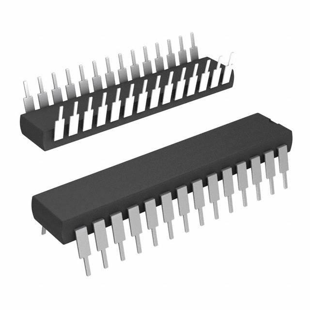
Hermetic 28-Lead Ceramic DIP, or Die
CMOS Input/Output Buffers
SIMPLIFIED FUNCTIONAL BLOCK DIAGRAM
A[0-14]
Row
Driver
Memory Array
Column
Decoder
NWE
NOE
CE (1)
NCS
DQ[0-7]
(1) CE input is not available in 28 lead DIP package, and CE is not supported for the
HT6256 in die form. For deliverable die user must connect CE to VDD.
28 LEAD PACKAGE PINOUT
�HT6256
SIGNAL DEFINITIONS
Pin
Name
Timing Definition
Symbol
A[0-14]
A
Address input pins. Selects a particular 8-bit word within the memory array.
DQ[0-7]
D
Q
Bi-directional data I/O pins. Data inputs (D) during a write operation. Data outputs (Q)
during a read operation.
NCS
S
Negative chip select. Low allows normal read or write operation. High puts the SRAM into
a deselected condition and holds the data output drivers in a high impedance (High-Z)
state. If not used, it must be connected to VSS.
NWE
W
Negative write enable. Low activates a write operation and holds the data output drivers in
a high impedance (High-Z) state. High allows normal read operation.
NOE
G
Negative output enable. High holds the data output drivers in a high impedance (High-Z)
state. Low the data output driver state is defined by NCS, CE and NWE. If not used, it
must be connected to VSS.
CE
Chip Enable. This control input is wire-bonded to VDD in the 28 lead package. Use of the
CE signal as an enable input is not supported for the HT6256 in die form. For deliverable
die, the user must connect CE to VDD.
n/a
VDD
Power input. Supplies power to the SRAM.
VSS
Ground
TRUTH TABLE
NCS
NWE
NOE
Mode
DQ Mode
H
X
X
Deselected
High-Z
L
H
L
Read
Data Out
L
H
H
Read Standby
High-Z
L
L
X
Write
Data In
SPECIFICATIONS
ABSOLUTE MAXIMUM RATINGS (1)
Symbol
Parameter
Ratings
Min
Unit
Max
VDD
Positive Supply Voltage Referenced to VSS
-0.5
7.0
V
VIO
Voltage on Any Input or Output Pin Referenced to VSS
-0.5
VDD + 0.5
V
IOUT
Average Output Current
25
mA
TSTORE
Storage Temperature
-65
250
C
270
C
TSOLDER (2) Soldering Temperature
PD
(3) Package Power Dissipation
2.5
W
28-Lead DIP
10.0
C/W
Die
0.5
C/W
300
C
PJC
Package Thermal Resistance (Junction to Case)
VHBM
Electrostatic Discharge Protection Voltage (Human Body Model)
TJ
Junction Temperature
2000
V
(1) Stresses in excess of those listed above may result in immediate permanent damage to the device. These are stress ratings only and
operation at these levels is not implied. Frequent or extended exposure to absolute maximum conditions may affect device reliability.
(2) Maximum soldering temperature can be maintained for no more than 5 seconds.
(3) IDDSB power + IDDOP power + Output driver power due to external loading must not exceed this specification.
2
www.hightempsolutions.com
�HT6256
RECOMMENDED OPERATING CONDITIONS (1)
Symbol
Parameter
Limits
Unit
Min
Typ
Max
VDD
Positive Supply Voltage Referenced to VSS
4.5
5.0
5.5
V
TC
Case Temperature
-55
25
225
C
VIO
Voltage on Any Input or Output Pin Referenced to VSS
-0.3
VDD + 0.3
V
(1) Specifications listed in datasheet apply when operated under the Recommended Operating Conditions unless otherwise specified.
POWER PIN ELECTRICAL CHARACTERISTICS
Symbol
Parameter
IDDSB
IDDOPW
(1)(2)
IDDOPR
(1)(2)
IDDOPD
(1)(2)
IDR
Conditions
Static
Supply Current
VIH = VDD,
VIL = VSS,
DQ = High-Z
Dynamic
Supply Current
Selected, Write
Dynamic
Supply Current
Selected, Read
VIH = VDD,
VIL = VSS,
DQ = High-Z
VIH = VDD,
VIL = VSS,
DQ = High-Z
Dynamic
Supply Current
Deselected
VIH = VDD,
VIL = VSS,
DQ = High-Z
Data Retention
Supply Current
VDD = 2.5V
Typ(3)
Max
Unit
0.2
2.0
mA
1MHz
3.4
4
mA
1MHz
2.8
4
mA
20MHz
0.2
2.0
mA
500
uA
(1) All inputs switching. DC average current.
(2) All dynamic operating mode current measurements (IDDOPx) exclude standby mode current (IDDSB). The total power is the
sum of the power from the standby current (IDDSB), dynamic current (IDDOPx) and output driver current driving the output load
(3) Typical operating conditions: VDD=5.0V, TA=25ºC
SIGNAL PIN ELECTRICAL CHARACTERISTICS (1)(2)
Symbol
Parameter
Conditions
IIN
Input Leakage Current
VSS ≤ VIN ≤ VDD
IOZ
Output Leakage Current
DQ = High-Z
VIL
Low-Level Input Voltage
CMOS
VIH
High-Level Input Voltage
CMOS
VOL
Low-Level Output Voltage
CMOS
IOL = 6mA
VOH
High-Level Output Voltage
CMOS
IOH = -3mA
Min
Max
Unit
-5
5
uA
-10
10
uA
0.3 x VDD
V
0.7 x VDD
V
0.4
4.2
V
V
(1) Voltages referenced to VSS.
PIN CAPACITANCE (1)
Symbol
Parameter
Max
Unit
CIN
Input Capacitance
7
pF
Data I/O Capacitance
9
pF
CDQ
(1)
Maximum capacitance is verified as part of initial qualification only.
www.hightempsolutions.com
3
�HT6256
READ CYCLE TIMING CHARACTERISTICS (1)(2)
Symbol
Parameter
Limits
TAVAVR
Read Cycle Time
TAVQV
Address Valid to Output Valid Access Time
TAXQX
Address Change to Output Invalid Time
TSLQV
Chip Select to Output Valid Access Time
TSLQX
Chip Select to Output Low-Z Time
TSHQZ
Chip Select to Output High-Z Time
TGLQV
Output Enable to Output Valid Access Time
TGLQX
Output Enable to Output Low-Z Time
TGHQZ
Output Enable to Output High-Z Time
Min
Unit
Max
50
ns
50
3
ns
ns
50
5
ns
ns
20
ns
20
ns
0
ns
15
ns
(1) The timing specifications are referenced to the Timing Input / Output References diagrams and the
Timing Reference Load Circuit diagrams.
(2) NWE = High
READ CYCLE TIMING WAVEFORMS
TAVAVR
A
TAVQV
TSLQV
TAXQX
NCS
TSHQZ
TSLQX
Q
HIGH-Z
DATA VALID
TGLQX
TGLQV
TGHQZ
NOE
4
www.hightempsolutions.com
�HT6256
WRITE CYCLE TIMING CHARACTERISTICS (1)(2)(3)
Symbol
Parameter
Limits
TAVAVW
Write Cycle Time
50
ns
TWLWH
Start of Write to End of Write Pulse Width
45
ns
TSLWH
Chip Select to End of Write Time
45
ns
TDVWH
Data Input Valid to End of Write Time
35
ns
TAVWH
Address Valid to End of Write Time
45
ns
TWHDX
Data Input Hold after End of Write Time
0
ns
TAVWL
Address Valid Setup to Start of Write Time
0
ns
TWHAX
Address Valid Hold after End of Write Time
0
ns
TWLQZ
Start of Write to Output High-Z Time
TWHQX
End of Write to Output Low-Z Time
5
ns
End of Write to Start of Write Pulse Width
5
ns
Min
TWHWL
(4)
Unit
Max
15
ns
(1) The timing specifications are referenced to the Timing Input / Output References diagrams and the
Timing Reference Load Circuit diagrams. IBIS models should be used to evaluate timing under application load and conditions.
(2) For an NWE controlled write, NCS must be Low and CE must be High when NWE is Low.
(3) Can use NOE = High to hold Q in a High-Z state when NWE = High, NCS = Low and CE = High.
(4) Guaranteed but not tested.
WRITE CYCLE TIMING WAVEFORMS
TAVAVW
A
TAVWH
TWHAX
TAVWL
TWLWH
TWHWL
NWE
TWHQX
TWLQZ
Q
HIGH-Z
TDVWH
D
HIGH-Z
TWHDX
DATA VALID
TSLQX
TSLWH
TSHQZ
NCS
www.hightempsolutions.com
5
�HT6256
Typical Operating Current vs. Frequency
@ 225C
Typical Cycle Times vs. Temperature
TIMING REFERENCE LOAD CIRCUIT (CMOS)
VDD/2
50ohm
DUT
Output
Zo = 50ohm
30pF (1)
Notes
(1) Set to 5pF for T*QZ (Low-Z to High-Z) timing parameters.
6
www.hightempsolutions.com
�HT6256
FUNCTIONAL DESCRIPTION
SRAM Operation
SRAM operation is asynchronous. Operating modes
are defined in the Truth Table. Read operations can
be controlled by Address (A) or Chip Select (NCS).
Write operations can be controlled by Write Enable
(NWE) or Chip Select (NCS).
Read Operation
A read operation occurs when Chip Select (NCS) is
low and Write Enable (NWE) is high. The output
drivers are controlled independently by the Output
Enable (NOE) signal.
To control a read cycle with NCS where TSLQV is the
access time, all addresses must be valid TAVQV
minus TSLQV prior to the enabling NCS transition.
Address transitions can occur later; however, the valid
Data Output (Q) access time will then be defined by
TAVQV instead of TSLQV. NCS can disable the read
at any time; however, Data Output drivers will enter a
High-Z state TSHQZ later.
To control a read cycle with Address where TAVQV is
the access time, NCS must transition to active TSLQV
minus TAVQV prior to the last Address transition. The
NCS active transition can occur later; however, the
valid Data Output (Q) access time will then be defined
by TSLQV instead of TAVQV. To perform consecutive
read cycles, NCS is held continuously low/high, and
the toggling of any Address will start a new read cycle.
Any amount of toggling or skew between Address
transitions is permissible; however, Data Output will
not become valid until TAVQV following the last
occurring Address transition. The minimum Address
activated read cycle time is TAVAVR which is the time
between the last Address transition of the previous
cycle and the first Address transition of the next cycle.
The valid Data Output from a previous cycle will
remain valid until TAXQX following the first Address
transition of the next cycle.
Write Operation
A write operation occurs when Write Enable (NWE)
and Chip Select (NCS) are low. The write mode can
be controlled via two different control signals: NWE or
NCS can start the write mode and end the write mode,
but the write operation itself is defined by the overlap
of NWE low, and NCS low. Both modes of control are
similar, except the NCS mode deselects the SRAM
when NCS is high between writes.
www.hightempsolutions.com
To write Data (D) into the SRAM, NWE and NCS must
be held low for at least TWLWH and TSLSH
respectively. Any amount of skew between these
signal transitions can be tolerated, and any one of
these control signals can start or end the write
operation as long as there is sufficient overlap in these
signals to ensure a valid write time (e.g., TSLWH and
TWLSH).
Address inputs must be valid at least TAVWL/TAVSL
before the start of write and TAVWH/TAVSH before
the end of write and must remain valid during the write
operation. Hold times for address inputs with respect
to the end of write must be a minimum of
TWHAX/TSHAX.
A Data Input (D) valid to the end of write time of
TDVWH/TDVSH must be provided during the write
operation. Hold times for Data Input with respect to the
end of write must be at least TWHDX/TSHDX. To
avoid Data Input driver contention with the SRAM
output driver, the Data Input (D) must not be applied
until TWLQZ/TGHQZ/TSHQZ after the output drive
(Q) is put into a High-Z condition by NWE/NOE/NCS.
Consecutive write cycles are performed by toggling at
least one of the start of write control signals for
TWHWL/TSHSL. If only one of these signals is used,
the other two must be in their write enable states. The
minimum write cycle time is TAVAVW/TAVAVS.
Signal Integrity
As a general design practice, one should have good
signal integrity which means input signals that are free
of noise, glitches and ringing with rising and falling
edges of ≤10ns. More specifically, an input is
considered to have good signal integrity when the
input voltage monotonically traverses the region
between VIL and VIH in ≤10ns. This is especially
important in a selected and enabled state. When the
device is selected and enabled, the last transitioning
input for the desired operation must have good signal
integrity to maintain valid operation. The transitioning
inputs that bring the device into and out of a selected
and enabled state must also have good signal integrity
to maintain valid operation. When the device is
deselected and/or disabled, inputs can have poor
signal integrity and even float as long as the inputs that
are defining the deselected and/or disabled state stay
within valid VIL and VIH voltage levels. However,
floating inputs for an extended period of time is not
recommended.
7
�HT6256
PACKAGING
The standard package is a hermetic 28-lead DIP constructed of multilayer ceramic (AI2O3) and features internal
power and ground planes. Ceramic chip capacitors can be mounted on the package by the user to maximize
supply noise decoupling and increase board packing density. These capacitors connect to the internal package
power and ground planes. This design minimized resistance and inductance of the bond wire and package. For
other packaging options or external control of Chip Enable (CE), call Honeywell.
28-LEAD DIP PACKAGE
C
D
Z
All dimensions in inches
Y
Right
Reading
on Lid
Ceramic
Body
A
1
E
Optional
Capacitors
X
Q
L
b2
b
(width)
eA
A
b
b2
C
D
E
e
eA
L
Q
X
Y
Z
0.175 (max)
0.018 ± 0.002
0.050 (typ)
0.009 to 0.012
1.400 ± 0.014
0.595 ± 0.010
0.100 ±0.005
0.600 ±0.010
0.125 to 0.175
0.050 ±0.010
0.130 ref
0.050 ref
0.075 ref
e
(pitch)
PACKAGE LEVEL SCREENING
The HT6256 package screening includes assembly screening (die-bond and wire-bond adhesion testing, pre-cap
visual inspection, and hermetic seal leak checking). Post-assembly electrical screening includes initial electrical
test, dynamic burn-in at 250C, and final electrical testing at -55C, 25C, and 225C.
8
www.hightempsolutions.com
�HT6256
DIE DETAIL
Die Dimension (millimeters)
A
D
E
Min.
0.655
-----
Nom.
0.675
6.955
7.295
Max.
0.695
-----
Notes:
(1) Backside metalization is gold.
(2) Metalization on the pads is aluminum.
(3) The backside of the die is connected to VSS.
www.hightempsolutions.com
9
�HT6256
DIE PAD DIMENSIONS AND TERMINAL CONNECTIONS
Die Pad
Number
1
2
3
4
5
6
7
8
9
10
11
12
13
14
15
16
17
18
19
20
21
22
23
24
25
26
27
28
29
30
31
32
33
34
35
Terminal
Connection
VSS
NOE
A11
A9
A8
A13
VSS
NWE
VDD
A14
A12
A7
A6
A5
A4
A3
VSS
VSS
A2
A1
A0
D0
D1
D2
VSS
D3
D4
D5
D6
D7
NCS
A10
CE
VDD
VSS
Pad Dimensions (millimeters)
X
Y
0.139
0.080
0.129
0.100
0.129
0.119
0.129
0.119
0.129
0.119
0.129
0.119
0.129
0.119
0.129
0.119
0.129
0.233
0.129
0.119
0.129
0.119
0.129
0.119
0.129
0.119
0.129
0.119
0.129
0.119
0.129
0.100
0.129
0.080
0.129
0.080
0.129
0.100
0.129
0.119
0.129
0.119
0.129
0.119
0.129
0.119
0.129
0.119
0.129
0.233
0.129
0.119
0.129
0.119
0.129
0.119
0.129
0.119
0.129
0.119
0.129
0.119
0.129
0.119
0.129
0.100
0.129
0.216
0.139
0.080
ASSEMBLY INFORMATION FOR DIE
Die Bonding
Honeywell recommends using a Eutectic Gold/Silicon perform or high temperature conductive adhesive for die
bonding to a ceramic package.
Wire Bonding
Aluminum bond wires must be used to achieve high temperature reliability. Wirebond the power and ground
pads before the other signal pads.
10
www.hightempsolutions.com
�HT6256
DIE LEVEL SCREENING
The HT6256 die are specified to operate over the entire temperature range. To meet this objective, three levels of
screening are in place.
1. Wafer Level – Each die is 100% electrical tested at room temperature.
2. Sample Package Test – A sample of die from each wafer are assembled into packages and screened
over the temperature range of -55C to +225C to verify performance.
3. The sample packaged parts also receive 44 hours of burn-in at 250C.
RELIABILITY
Honeywell understands the stringent reliability requirements for extreme environment systems and has extensive
experience in reliability testing on programs of this nature. Reliability attributes of the HTMOS™ process were
characterized by testing test structures from which specific failure mechanisms were evaluated. These specific
mechanisms included, but were not limited to, hot carriers, electromigration, and time dependent dielectric
breakdown. This data was then used to make changes to the design models and process to ensure reliable -55
to +225ºC specified products.
ORDER INFORMATION
H
T
Process
T = Hi Temp SOI
x
6256
Part Type
6256 = SRAM
Source
Package
H = Honeywell
D = 28-lead DIP
Z = Die
Honeywell reserves the right to make changes to improve reliability, function or design. Honeywell does not assume any liability arising out of
the application or use of any product or circuit described herein; neither does it convey any license under its patent rights nor the rights of
others.
Honeywell International Inc.
12001 Highway 55
Plymouth, MN 55441
Tel: 800-323-8295
www.hightempsolutions.com
www.hightempsolutions.com
ADS-14253
November 2015
©2015 Honeywell International Inc.
11
�


 工商网监
湘ICP备2023018690号
工商网监
湘ICP备2023018690号
