Agilent ABA-32563 2.5 GHz Broadband Silicon RFIC Amplifier
Data Sheet
Features • Operating Frequency DC ~ 2.5 GHz • 19 dB Gain • VSWR < 2.0 throughout operating frequency • 8.4 dBm Output P1dB Description Agilent’s ABA-32563 is an economical, easy-to-use, internally 50Ω matched, silicon monolithic broadband amplifier that offers excellent gain and broadband response from DC to 2.5 GHz. Packaged in an ultraminiature SOT-363 package, it requires half the board space of a SOT-143 package. At 2 GHz, the ABA-32563 offers a small-signal gain of 19 dB, output P1dB of 8.4 dBm and 19.5 dBm output third order intercept point. It is suitable for use as wideband applications. They are designed for low cost gain blocks in cellular applications, DBS tuners, LNB and other wireless communication systems. ABA-32563 is fabricated using Agilent’s HP25 silicon bipolar process, which employs a doublediffused single polysilicon process with self-aligned submicron emitter geometry. The process is capable of simultaneous high fT and high NPN breakdown (25 GHz fT at 6V BVCEO). The process utilizes industry standard device oxide isolation technologies and submicron aluminum multilayer interconnect to achieve superior performance, high uniformity, and proven reliability. Surface Mount Package SOT-363/SC70 • 19.5 dBm Output IP3 • 3.5 dB Noise Figure • Unconditionally Stable • Single 3V Supply (Id = 37 mA) • Lead-free Applications • Amplifier for Cellular, Cordless, Special Mobile Radio, PCS, ISM, Wireless LAN, DBS, TVRO, and TV Tuner Applications
Pin Connections and Package Marking
GND 1 Output & Vcc
2Kx
GND 2 Input
GND 3 Vcc
Attention: Observe precautions for handling electrostatic sensitive devices.
ESD Machine Model (Class A) ESD Human Body Model (Class 1B) Refer to Agilent Application Note A004R: Electrostatic Discharge Damage and Control.
Note: Top View. Package marking provides orientation and identification. “x” is the date code.
Simplified Schematic
Vcc RF Output & Vcc
RF Input
Ground 2
Ground 3
Ground 1
�ABA-32563 Absolute Maximum Ratings [1] Symbol
Vcc Pin Pdiss Tj TSTG
Parameter
Device Voltage, RF output to ground (T = 25°C) CW RF Input Power (Vcc = 3V) Total Power Dissipation [3] Junction Temperature Storage Temperature
Units
V dBm W °C °C
Absolute Max.
6 15 0.6 150 -65 to 150
Thermal Resistance[2] (Vcc = 3V) θj-c = 124.3°C/W
Notes: 1. Operation of this device in excess of any of these limits may cause permanent damage. 2. Thermal resistance measured using 150°C Liquid Crystal Measurement Technique. 3. Board (package belly) temperature, Tc, is 25°C. Derate 8.1 mW/°C for Tc > 120.8°C.
Electrical Specifications
Tc = +25°C, Zo = 50 Ω, Pin = -30 dBm, Vcc = 3V, Freq = 2 GHz, unless stated otherwise.
Symbol
Gp[1] ∆Gp NF[1] P1dB[1] OIP3[1] VSWRin[1] VSWRout Icc[1] Td[1]
[1]
Parameter and Test Condition
Power Gain (|S21|2 ) Power Gain Flatness, Noise Figure Output Power at 1dB Gain Compression Output Third Order Intercept Point Input VSWR Output VSWR Device Current Group Delay f = 0.1 ~ 1.5 GHz f = 0.1 ~ 2.5 GHz
Units
dB dB dB dBm dBm
Min.
17.5
Typ.
19.0 1.0 3.0 3.5 8.4 19.5
很抱歉,暂时无法提供与“ABA-32563-TR1G”相匹配的价格&库存,您可以联系我们找货
免费人工找货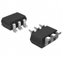


 工商网监
湘ICP备2023018690号
工商网监
湘ICP备2023018690号
