Agilent AMMP-5618 6–20 GHz General Purpose Amplifier
Data Sheet
Features • 5 x 5 mm surface mount package • Broad band performance 6 – 20 GHz • High +19 dBm output power • Medium 13 dB typical gain • 50Ω input and output match Description Agilent’s AMMP-5618 is a high power, medium gain amplifier that operates from 6 GHz to 20 GHz. The amplifier is designed to be an easy-to-use component for any surface mount PCB application. In communication systems, it can be used as a LO buffer, or as a transmit driver amplifier. During typical operation with a single 5V supply, each gain stage is biased for Class-A operation for optimal power output with minimal distortion. The amplifier has integrated 50Ω I/O match, DC blocking, self-bias and choke to eliminate complex tuning and assembly processes typically required by hybrid (discrete-FET) amplifiers. The package is fully SMT compatible with backside grounding and I/O to simplify assembly. Note: These devices are ESD sensitive. The following precautions are strongly recommended. Ensure that an ESD approved carrier is used when dice are transported from one destination to another. Personal grounding is to be worn at all times when handling these devices.
Vd 1 2 3
• Single 5V (107 mA) supply bias
RFin 8
4 RFout
Applications • Microwave radio systems • Satellite VSAT, DBS up/down link
7
6
5
• LMDS & Pt-Pt mmW long haul • Broadband wireless access (including 802.16 and 802.20 WiMax) • WLL and MMDS loops • Commercial grade military
Attention: Observe precautions for handling electrostatic sensitive devices.
ESD Machine Model (Class A) ESD Human Body Model (Class 0) Refer to Agilent Application Note A004R: Electrostatic Discharge Damage and Control.
Absolute Maximum Ratings [1]
Symbol
Vd Id Pin Tch Tstg Tmax
Parameters/Conditions
Positive Drain Voltage Drain Current CW Input Power Operating Channel Temperature Storage Case Temperature Max. Assembly Temp (60 sec max)
Units
V mA dBm °C °C °C
Min.
Max.
7 150 20 +150
-65
+150 +300
Note: 1. Operation in excess of any one of these conditions may result in permanent damage to this device.
�AMMP-5618 DC Specifications/Physical Properties[1]
Symbol
Id θch-b
Parameters and Test Conditions
Drain Supply Current (under any RF power drive and temperature) (Vd=5.0V) Thermal Resistance[2] (Backside temperature, T
b = 25°C)
Units
mA °C/W
Min.
Typ.
107 34
Max.
140
Notes: 1. Ambient operational temperature TA = 25°C unless otherwise noted. 2. Channel-to-backside Thermal Resistance (Tchannel (Tc) = 34°C) as measured using infrared microscopy. Thermal Resistance at backside temperature (Tb) = 25°C calculated from measured data.
RF Specifications[3,4,6] (TA = 25°C, Vd = 5.0V, Id(Q)= 107 mA, Zo =50 Ω) Symbol
Gain NF P-1dB OIP3 RLin RLout Isol
Parameters and Test Conditions
Small-signal Gain [5] Noise Figure into 50Ω [5] Output Power at 1 dB Gain Compression Third Order Intercept Point; ∆f = 100 MHz; Pin = -20 dBm Input Return Loss Output Return Loss Reverse Isolation
Units
dB dB dBm dBm dB dB dB
Typ.
13 4.4 +19 +30 -12 -12 -40
Sigma
0.4 0.2 0.9 1.2 0.7 0.6 1.2
Notes: 3. Small/Large -signal data measured in a fully de-embedded test fixture form TA = 25°C. 4. Pre-assembly into package performance verified 100% on-wafer per AMMC-5618 published specifications 5. This final package part performance is verified by a functional test correlated to actual performance at one or more frequencies 6. Specifications are derived from measurements in a 50Ω test environment. Aspects of the amplifier performance may be improved over a more narrow bandwidth by application of additional conjugate, linearity, or low noise (Γopt) matching.
2
�AMMP-5618 Typical Performance (TA = 25°C, Vd = 5V, Id = 107 mA, Z in = Z out = 50Ω unless otherwise stated)
Note: These measurements are in 50Ω test environment. Aspects of the amplifier performance may be improved over a narrower bandwidth by application of additional conjugate, linearity or low noise (Γopt) matching.
15 0 0 -5 -10
S21 (dB) S12 (dB) S11 (dB)
12
-10
9
-20
-15 -20
6
-30
3
-40
-25 -30 4 6 8 10 12 14 16 18 20 22 4 6 8 10 12 14 16 18 20 22 FREQUENCY (GHz) FREQUENCY (GHz)
0 4 6 8 10 12 14 16 18 20 22 FREQUENCY (GHz)
-50
Figure 1. Gain.
Figure 2. Isolation.
Figure 3. Input Return Loss.
0 -5 -10
S22 (dB)
8
35 30
7 25
NF (dB) OP-1dB (dBm)
6
20 15 10
-15 -20 -25 -30 4 6 8 10 12 14 16 18 20 22 FREQUENCY (GHz)
5
4 5 3 6 8 10 12 14 16 18 20 FREQUENCY (GHz) 0
OP1dB OIP3 6 8 10 12 14 16 18 20
FREQUENCY (GHz)
Figure 4. Output Return Loss.
Figure 5. Noise Figure.
Figure 6. Typical Power, OP-1dB and OIP3.
20
0 -10 -20 25°C -40°C +85°C
S11 (dB)
0 25°C -40°C +85°C
15
-5
S21 (dB)
S12 (dB)
10
-30 -40
-10
5 25°C -40°C +85°C
-15 -50 -60 -20 4 6 8 10 12 14 16 18 20 22 4 6 8 10 12 14 16 18 20 22 FREQUENCY (GHz) FREQUENCY (GHz)
0
-5 4 6 8 10 12 14 16 18 20 22 FREQUENCY (GHz)
Figure 7. Gain Over Temperature.
Figure 8. Isolation Over Temperature.
Figure 9. Input RL Over Temperature.
3
�AMMP-5618 Typical Performance (TA = 25°C, Vd = 5V, Id = 107 mA, Z in = Z out = 50Ω unless otherwise stated)
Note: These measurements are in 50Ω test environment. Aspects of the amplifier performance may be improved over a narrower bandwidth by application of additional conjugate, linearity or low noise (Γopt) matching.
0 -5 -10 25°C -40°C +85°C 8 25°C -40°C +85°C 108 106 104
7
S21 (dB)
NF (dB)
6
-15 -20 -25 -30
Idd (mA)
102 100 98 25°C -40°C +85°C 3 3.5 4 Vdd (V) 4.5 5
5
4 96 3 4 6 8 10 12 14 16 18 20 22 6 8 10 12 14 16 18 20 FREQUENCY (GHz) FREQUENCY (GHz) 94
Figure 10. Output Return Loss Over Temperature.
16
Figure 11. NF Over Temperature.
Figure 12. Bias Current Over Temperature.
0 -10 3V 4V 5V
0 3V 4V 5V
12 -20
-5
S21 (dB)
S12 (dB)
8
-30 -40
S11 (dB)
4 6 8 10 12 14 16 18 20
-10
4
3V 4V 5V
-15 -50 -60 -20 4 6 8 10 12 14 16 18 20 FREQUENCY (GHz)
0
4
6
8
10
12
14
16
18
20
22
FREQUENCY (GHz)
FREQUENCY (GHz)
Figure 13. Gain Over Vdd.
Figure 14. Isolation Over Vdd.
Figure 15. Input RL Over Vdd.
0 -5 -10 3V 4V 5V
20
35 30
16 25
OP-1dB (dBm)
S22 (dB)
-15 -20 -25
12
OIP3 (dBm)
3V 4V 5V 6 8 10 12 14 16 18 20
20 15 10 5 0 3V 4V 5V 6 8 10 12 14 16 18 20
8
4 -30 -35 0 4 6 8 10 12 14 16 18 20 FREQUENCY (GHz) FREQUENCY (GHz)
FREQUENCY (GHz)
Figure 16. Output Return Loss Over Vdd.
Figure 17. Output Power Over Vdd.
Figure 18. OIP3 Over Vdd.
4
�AMMP-5618 Typical Scattering Parameters[1] (TA = 25°C, Vd = 5 V, ZO = 50Ω)
Freq. GHz
2.0 2.5 3.0 3.5 4.0 4.5 5.0 5.5 6.0 6.5 7.0 7.5 8.0 8.5 9.0 9.5 10.0 10.5 11.0 11.5 12.0 12.5 13.0 13.5 14.0 14.5 15.0 15.5 16.0 16.5 17.0 17.5 18.0 18.5 19.0 19.5 20.0 20.5 21.0 21.5 22.0 22.5 23.0 23.5 24.0 24.5 25.0
dB
-2.995 -3.432 -4.250 -4.096 -4.325 -4.797 -6.417 -11.055 -18.578 -23.802 -25.186 -27.287 -27.021 -24.540 -23.582 -23.477 -24.304 -22.475 -19.215 -16.258 -14.234 -13.024 -12.514 -12.482 -12.919 -13.636 -13.993 -13.835 -13.000 -12.524 -12.067 -11.963 -12.862 -12.547 -11.062 -10.610 -10.469 -10.018 -9.997 -10.136 -9.631 -7.870 -5.619 -4.449 -4.155 -4.196 -4.530
S11 Mag
0.708 0.674 0.613 0.624 0.608 0.576 0.478 0.280 0.118 0.065 0.055 0.043 0.045 0.059 0.066 0.067 0.061 0.075 0.109 0.154 0.194 0.223 0.237 0.238 0.226 0.208 0.200 0.203 0.224 0.236 0.222 0.200 0.181 0.187 0.225 0.272 0.300 0.316 0.316 0.311 0.330 0.404 0.524 0.599 0.620 0.617 0.594
Phase
70.854 7.524 -59.292 -112.628 -174.493 121.652 52.449 -16.473 -62.704 -78.360 -114.355 176.586 89.220 16.508 -43.865 -104.344 -175.038 107.849 44.619 -5.409 -51.554 -95.001 -138.454 177.883 132.024 87.229 38.470 -5.903 -52.805 -103.865 -152.985 153.118 93.198 28.065 -33.067 -88.132 -138.271 173.388 122.816 65.257 -1.277 -59.633 -127.317 171.791 119.140 71.146 23.384
dB
-22.696 -16.093 -4.538 -1.726 0.287 5.870 10.805 13.764 14.224 14.468 14.500 14.416 14.509 14.512 14.512 14.523 14.491 14.473 14.479 14.388 14.419 14.367 14.328 14.202 14.147 13.972 14.029 13.739 13.725 13.966 14.024 14.002 14.148 14.132 14.210 14.091 13.858 13.623 13.398 13.019 12.886 12.504 11.738 10.831 9.293 8.021 6.897
S21 Mag
0.073 0.157 0.593 0.461 0.394 1.131 3.164 4.712 5.385 5.475 5.495 5.506 5.501 5.503 5.503 5.510 5.490 5.479 5.482 5.425 5.382 5.350 5.326 5.249 5.216 5.054 4.971 4.920 4.969 5.109 5.143 5.130 5.217 5.207 5.254 5.183 5.046 4.911 4.785 4.797 4.724 4.219 3.863 3.480 2.915 2.518 2.212
Phase
45.614 62.385 -0.007 -157.105 -52.399 -107.307 -175.227 108.456 38.847 -23.228 -75.874 -127.412 -176.352 134.523 87.924 41.684 -3.914 -48.272 -93.057 -137.014 179.443 136.208 92.923 50.240 6.926 -35.308 -77.276 -118.133 -158.923 158.580 115.249 72.656 29.105 -14.187 -58.599 -104.365 -149.000 165.396 122.433 77.749 29.934 -13.003 -63.650 -112.183 -157.885 159.348 116.230
dB
-58.670 -49.826 -43.091 -36.349 -39.160 -42.543 -50.015 -46.815 -42.183 -40.719 -39.954 -39.602 -39.264 -39.039 -38.938 -38.808 -38.711 -38.711 -38.700 -38.773 -38.489 -38.221 -38.071 -37.739 -37.252 -37.903 -37.680 -38.692 -39.424 -38.107 -37.443 -37.604 -37.848 -38.170 -38.384 -39.112 -39.698 -40.748 -42.165 -43.928 -45.145 -49.217 -47.596 -53.021 -51.322 -46.344 -45.149
S12 Mag
0.001 0.003 0.007 0.015 0.011 0.007 0.003 0.005 0.008 0.009 0.010 0.010 0.011 0.011 0.011 0.011 0.012 0.012 0.012 0.012 0.012 0.012 0.012 0.013 0.014 0.013 0.013 0.012 0.011 0.012 0.013 0.013 0.013 0.012 0.012 0.011 0.010 0.009 0.008 0.006 0.006 0.003 0.004 0.002 0.003 0.005 0.006
Phase
91.028 -30.565 172.431 -48.599 -129.213 166.320 130.192 155.918 114.699 69.159 27.235 -12.197 -50.735 -88.381 -124.530 -160.536 163.632 128.550 92.021 61.222 26.022 -8.975 -43.893 -78.798 -114.505 -153.055 172.112 133.007 104.224 82.267 37.833 0.928 -35.629 -72.292 -109.537 -147.597 176.777 139.612 102.558 74.095 49.307 -1.915 -40.229 -136.023 114.374 21.965 -35.249
dB
-0.537 -0.694 -1.503 -3.848 -4.217 -5.052 -6.475 -8.555 -10.393 -12.156 -14.372 -17.196 -18.937 -17.986 -16.383 -15.281 -14.875 -15.430 -16.520 -18.494 -20.529 -22.659 -24.039 -24.607 -24.958 -26.020 -25.949 -25.799 -23.027 -21.872 -21.936 -22.039 -22.843 -24.452 -24.014 -20.632 -16.990 -13.793 -11.540 -9.819 -8.659 -7.188 -7.034 -7.133 -7.517 -8.346 -9.765
S22 Mag
0.940 0.923 0.841 0.642 0.615 0.559 0.475 0.373 0.302 0.247 0.191 0.138 0.113 0.126 0.152 0.172 0.180 0.169 0.149 0.119 0.094 0.074 0.063 0.059 0.057 0.050 0.050 0.051 0.071 0.081 0.080 0.079 0.072 0.060 0.063 0.093 0.141 0.204 0.265 0.323 0.369 0.437 0.445 0.440 0.421 0.383 0.325
Phase
118.786 56.844 -77.196 -20.982 -101.456 -168.104 130.723 79.201 36.021 -7.111 -54.746 -111.340 -179.767 115.789 65.272 25.081 -11.906 -47.630 -83.772 -122.670 -163.935 150.698 107.199 69.051 37.568 10.165 -2.864 -10.215 -27.632 -63.932 -90.189 -122.785 -163.441 144.595 83.275 30.364 -10.504 -47.217 -83.538 -119.330 -153.160 166.236 131.591 97.415 61.706 22.766 -21.448
Note: 1. Data obtained from in fixture de-embedded to package edge.
Input Reference Plane Input Reference Plane for s-parameters for s-parameters
Output Reference OutputReference Plane Plane for s-parameters for s-parameters. (View from package bottom)
5
�Biasing and Operation The AMMC-5618 is normally biased with a single positive drain supply connected to both VD pins through bypass capacitors as shown in Figure 19. The recommended supply voltage is 5V. It is important to have 0.1 µF bypass capacitor, and the capacitor should be placed as close to the component as possible.
The AMMC-5618 does not require a negative gate voltage to bias any of the three stages. No ground wires are needed because all ground connections are made with plated through-holes to the backside of the package. Refer to the Absolute Maximum Ratings table for allowed DC and thermal conditions.
Figure 21. Demonstration Board (available upon request).
Vd (Typ 5V)
0.1 µF
1
2
3
RFin
8
4
RFout
7
6
5
BASE GND
Figure 19. Typical Application.
VD1
VD2
Feedback Network
Feedback Network
Matching
RF Input
Matching
Matching
RF Output
VG1
VG2
Figure 20. Simplified MMIC Schematic.
6
�1
23
.200 [5.08]
8
4
Recommended SMT Attachment The AMMP Packaged Devices are compatible with high volume surface mount PCB assembly processes. The PCB material and mounting pattern, as defined in the data sheet, optimizes RF performance and is strongly recommended. An electronic drawing of the land pattern is available upon request from Agilent Sales & Application Engineering. Manual Assembly 1. Follow ESD precautions while handling packages. 2. Handling should be along the edges with tweezers. 3. Recommended attachment is conductive solder paste. Please see recommended solder reflow profile. Conductive epoxy is not recommended. Hand soldering is not recommended. 4. Apply solder paste using a stencil printer or dot placement. The volume of solder paste will be dependent on PCB and component layout and should be controlled to ensure consistent mechanical and electrical performance. 5. Follow solder paste and vendor’s recommendations when developing a solder reflow profile. A standard profile will have a steady ramp up from room temperature to the pre-heat temperature to avoid damage due to thermal shock. 6. Packages have been qualified to withstand a peak temperature of 260° C for 20 seconds. Verify that the profile will not expose device beyond these limits.
7
65 .075 [1.91]
.200 [5.08]
Front View
Side View
.011 [0.28] .018 [0.46]
.114 [2.9] .014 [0.365] 321 .016 [0.40]
.126 [3.2]
4 .059 [1.5] .100 [2.54]
8 .012 [0.30] 5 67 .028 [0.70]
.029 [0.75] .100 [2.54] .016 [0.40] .093 [2.36]
Dimensional Tolerances: 0.002" [0.05 mm]
Back View Notes: 1. * Indicates Pin 1 2. Dimensions are in inches [millimeters] 3. All Grounds must be soldered to PCB RF Ground
Figure 22. Outline Drawing.
.093 [2.36] .010 [0.25] .011 [0.28] .016 [0.40] .0095 [0.24]
.016 [0.40] .126 [3.20] .059 [1.50] .020 [0.50] .012 [0.3]
.018 [0.46] .018 [0.46] .114 [2.90]
.0095 [0.24]
Figure 23. Suggested PCB Material and Land Pattern.
7
�Solder Reflow Profile The most commonly used solder reflow method is accomplished in a belt furnace using convection heat transfer. The suggested reflow profile for automated reflow processes is shown in Figure 24. This profile is designed to ensure reliable finished joints. However, the profile indicated in Figure 1 will vary among different solder pastes from different manufacturers and is shown here for reference only.
Stencil Design Guidelines A properly designed solder screen or stencil is required to ensure optimum amount of solder paste is deposited onto the PCB pads. The recommended stencil layout is shown in Figure 25. The stencil has a solder paste deposition opening approximately 70% to 90% of the PCB pad. Reducing stencil opening can potentially generate more voids underneath. On the other hand, stencil openings larger than 100% will
lead to excessive solder paste smear or bridging across the I/O pads. Considering the fact that solder paste thickness will directly affect the quality of the solder joint, a good choice is to use a laser cut stencil composed of 0.127 mm (5 mils) thick stainless steel which is capable of producing the required fine stencil outline. The combined PCB and stencil layout is shown in Figure 26.
300 Peak = 250 ± 5°C 250 Melting point = 218°C
Temp (°C)
200 150 100 50 0 0 Ramp 1 50 Preheat 100 Ramp 2 150 Reflow 200 Cooling 250 300
Seconds
Figure 24. Suggested Lead-Free Reflow Profile for SnAgCu Solder Paste.
0.40
0.70
0.60 0.67
0.46
0.60 1.60 0.9550
3.20 1.80 0.40 0.36 0.30 0.36 0.40
0.95 0.36 1.80
0.36 0.27
0.27
0.36 0.40 4x - R0.14
1.60 2.90 Stencil Opening
Figure 25. Stencil Outline Drawing (mm).
Figure 26. Combined PCB and Stencil Layouts (mm).
8
�Part Number Ordering Information
Part Number AMMP-5618-BLK AMMP-5618-TR1 AMMP-5618-TR2 Devices per Container 10 100 500 Container antistatic bag 7” Reel 7” Reel
Device Orientation (Top View)
Carrier Tape and Pocket Dimensions
www.agilent.com/semiconductors
For product information and a complete list of distributors, please go to our web site. For technical assistance call: Americas/Canada: +1 (800) 235-0312 or (916) 788-6763 Europe: +49 (0) 6441 92460 China: 10800 650 0017 Hong Kong: (65) 6756 2394 India, Australia, New Zealand: (65) 6755 1939 Japan: (+81 3) 3335-8152(Domestic/International), or 0120-61-1280(Domestic Only) Korea: (65) 6755 1989 Singapore, Malaysia, Vietnam, Thailand, Philippines, Indonesia: (65) 6755 2044 Taiwan: (65) 6755 1843 Data subject to change. Copyright © 2005 Agilent Technologies, Inc. January 31, 2005 5989-1994EN
�
很抱歉,暂时无法提供与“AMMP-5618-TR2”相匹配的价格&库存,您可以联系我们找货
免费人工找货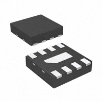


 工商网监
湘ICP备2023018690号
工商网监
湘ICP备2023018690号
