3A, 52kHz, Step-Down Switching Regulator
FEATURES
LM2576
SOP8-PP PKG
z 3.3V, 5.0V, 12V and Adjustable Output Versions
z Adjustable Version Output Voltage Range, 1.23 to 37V
+/- 4% AG10Maximum Over Line and Load Conditions
z Guaranteed 3.0A Output Current
z Wide Input Voltage Range
z Requires Only 4 External Components
z 52kHz Fixed Frequency Internal Oscillator
z TTL Shutdown Capability, Low Power Standby Mode
z High Efficiency
z Uses Readily Available Standard Inductors
z Thermal Shutdown and Current Limit Protection
z Moisture Sensitivity Level 3 for SMD packages
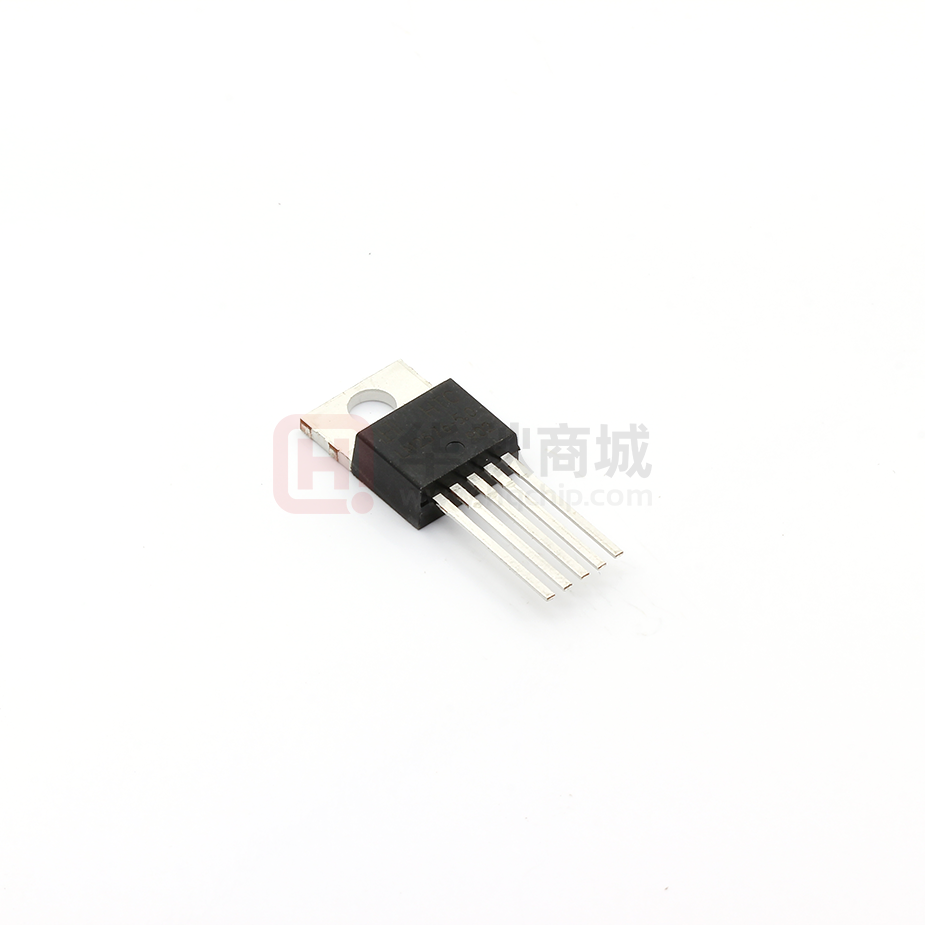
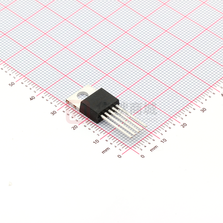
TO-220 PKG
TO-263 PKG
APPLICATION
z
z
z
z
z
z
Simple High-Efficiency Step-Down(Buck) Regulator
Efficient Pre-Regulator for Linear Regulators
On-Card Switching Regulators
Positive to Negative Converter(Buck-Boost)
Negative Step-Up Converters
Power Supply for Battery Chargers
ORDERING INFORMATION
Device
LM2576DP-X.X
LM2576T-X.X
LM2576R-X.X
Marking
LM2576-X.X
LM2576-X.X
LM2576-X.X
Package
SOP8-PP
TO-220
TO-263
DESCRIPTION
The LM2576 series of regulators are monolithic integrated circuits ideally suited for easy and convenient
design of a step-down switching regulator (buck converter).
All circuits of this series are capable of driving a 3.0A load with excellent line and load regulation. These
devices are available in fixed output voltages of 3.3V, 5.0V, 12V and an adjustable output version.
These regulators were designed to minimize the number of external components to simplify the power supply
design. Standard series of inductors optimized for use with the LM2576 are offered by several different inductor
manufacturers.
Since the LM2576 converter is a switch-mode power supply, its efficiency is significantly higher in comparison
with popular three-terminal linear regulators, especially with higher input voltages.
In many cases, the power dissipated is so low that no heatsink is required or its size could be reduced
dramatically. A standard series of inductors optimized for use with the LM2576 are available from several
different manufacturers. This feature greatly simplifies the design of switch-mode power supplies. The LM2576
features include a guaranteed +/- 4% tolerance on output voltage within specified input voltages and output
load conditions, and +/-10% on the oscillator frequency (+/- 2% over 0˚C to 125˚C).
External shutdown is included, featuring 80㎂(typical) standby current. The output switch includes cyclebycycle current limiting, as well as thermal shutdown for full protection under fault conditions.
Dec 2011 – Rev. 1.3
-1
-
HTC
�3A, 52kHz, Step-Down Switching Regulator
LM2576
Ordering Information
VOUT
ADJ
3.3V
5.0V
12V
Package
Order No.
Description
Package Marking
Status
SOP8-PP
LM2576DP-ADJ
3A, Adjustable, 52kHz, On/off
LM2576-ADJ
Contact Us
TO220-5L
LM2576T-ADJ
3A, Adjustable, 52kHz, On/off
LM2576-ADJ
Active
TO263-5L
LM2576R-ADJ
3A, Adjustable, 52kHz, On/off
LM2576-ADJ
Active
SOP8-PP
LM2576DP-3.3
3A, Fixed, 52kHz, On/off
LM2576-3.3
Contact Us
TO220-5L
LM2576T-3.3
3A, Fixed, 52kHz, On/off
LM2576-3.3
Active
TO263-5L
LM2576R-3.3
3A, Fixed, 52kHz, On/off
LM2576-3.3
Active
SOP8-PP
LM2576DP-5.0
3A, Fixed, 52kHz, On/off
LM2576-5.0
Contact Us
TO220-5L
LM2576T-5.0
3A, Fixed, 52kHz, On/off
LM2576-5.0
Active
TO263-5L
LM2576R-5.0
3A, Fixed, 52kHz, On/off
LM2576-5.0
Active
SOP8-PP
LM2576DP-12
3A, Fixed, 52kHz, On/off
LM2576-12
Contact Us
TO220-5L
LM2576T-12
3A, Fixed, 52kHz, On/off
LM2576-12
Active
TO263-5L
LM2576R-12
3A, Fixed, 52kHz, On/off
LM2576-12
Active
LM
2576
Output Voltage : ADJ / 3.3V / 5.0V /12V
Package Type
DP : SOP8-PP
T : TO220-5L
R : TO263-5L
Root Name
Product Code
Dec 2011 – Rev. 1.3
-2
-
HTC
�3A, 52kHz, Step-Down Switching Regulator
LM2576
PIN CONFIGURATION
VIN
1
8 N.C
VOUT 2
FEEDBACK 3
ON/OFF
Exposed
7 N.C
PAD
6 GND
4
5 N.C.
SOP8-PP
TO220-5L
TO263-5L
PIN DESCRIPTION
Package
TO-220 5L
TO-263 5L
SOP8-PP
Symbol
1
1
VIN
2
2
VOUT
3
6
GND
4
3
FEEDBACK
5
4
ON/OFF
-
5, 7, 8
N.C.
Description
This pin is the positive input supply for the LM2576 step–down
switching regulator.
In order to minimize voltage transients and to supply the switching
currents needed by the regulator, a suitable input bypass capacitor
must be present. (Cin in Figure 1).
This is the emitter of the internal switch. The saturation voltage
VSAT of this output switch is typically 1.5V. It should be kept in mind
that the PCB area connected to this pin should be kept to a
minimum in order to minimize coupling to sensitive circuitry.
Circuit ground pin. See the information about the printed circuit
board layout.
This pin senses regulated output voltage to complete the feedback
loop.
The signal is divided by the internal resistor divider network R2, R1
and applied to the non–inverting input of the internal error amplifier.
In the adjustable version of the LM2576 switching regulator this pin
is the direct input of the error amplifier and the resistor network R2,
R1 is connected externally to allow programming of the output
voltage.
It allows the switching regulator circuit to be shutdown using logic
level signals, thus dropping the total input supply current to
approximately 80uA.
The threshold voltage is typically 1.4V. Applying a voltage above
this value (up to +Vin) shuts the regulator off. If the voltage applied
to this pin is lower than 1.4V or if this pin is left open, the regulator
will be in the "on" condition
No Connect.
* Exposed Pad of SOP8-PP package should be externally connected to GND.
Dec 2011 – Rev. 1.3
-3
-
HTC
�3A, 52kHz, Step-Down Switching Regulator
LM2576
Typical Application (Fixed Output Voltage Versions)
Figure 1. Block Diagram and Typical Application
Dec 2011 – Rev. 1.3
-4
-
HTC
�3A, 52kHz, Step-Down Switching Regulator
LM2576
ABSOLUTE MAXIMUM RATINGS
(Absolute Maximum Ratings indicate limits beyond which damage to the device may occur)
Rating
Symbol
Value
UNIT
Maximum Supply Voltage
Vin
45
V
On/Off Pin Input Voltage
-
-0.3V ≤ V ≤ +Vin
V
Output Voltage to Ground (Steady-State)
Power Dissipation
SOP8-PP 8Lead
Thermal Resistance, Junction to Ambient
Thermal Resistance, Junction to Case
TO-220 5Lead
Thermal Resistance, Junction to Ambient
Thermal Resistance, Junction to Case
TO-263 5Lead
Thermal Resistance, Junction to Ambient
Thermal Resistance, Junction to Case
Storage Temperature Range
Minimum ESD Rating(Human Body Model:
C=100 pF, R=1.5kΩ
Lead Temperature (Soldering, 10seconds)
-
-1.0
V
PD
θJA
θJC
PD
θJA
θJC
PD
θJA
θJC
TSTG
Internally Limited
Contact us
Contact us
Internally Limited
65
5
Internally Limited
70
5
-60 to +150
W
℃/W
℃/W
W
℃/W
℃/W
W
℃/W
℃/W
℃
-
2.0
kV
-
260
℃
TJ
150
℃
Maximum Junction Temperature
OPERATING RATINGS (Operating Ratings indicate conditions for which the device is intended to be
functional, but do not guarantee specific performance limits. For guaranteed specifications, see the
Electrical Characteristics.)
Rating
Symbol
Value.
Unit
Operating Junction Temperature Range
TJ
-40 to +125
℃
Supply Voltage
Vin
40
V
Dec 2011 – Rev. 1.3
-5
-
HTC
�3A, 52kHz, Step-Down Switching Regulator
LM2576
ELECTRICAL CHARACTERISTICS / SYSTEM PARAMETERS ([Note 1] Test Circuit Figure 15)
(Unless otherwise specified, Vin = 12V for the 3.3V, 5.0V, and Adjustable version, Vin = 25V for the 12V version.
ILoad = 500 mA. For typical values TJ = 25°C, for min/max values TJ is the operating junction temperature range
that applies [Note 2], unless otherwise noted.)
Characteristics
LM2576-3.3V ([Note 1] Test Circuit Figure 2)
Output Voltage (Vin = 12V, ILOAD=0.5A, TJ=25℃)
Output Voltage (6.0V≤Vin≤40V, 0.5A≤ILOAD≤3.0A
TJ=25℃
TJ= -40℃ ~ +125℃
Efficiency (Vin=12V, ILOAD=3.0A)
LM2576-5.0V ([Note 1] Test Circuit Figure 2)
Output Voltage (Vin = 12V, ILOAD=0.5A, TJ=25℃)
Output Voltage (8.0V≤Vin≤40V, 0.5A≤ILOAD≤3.0A
TJ=25℃
TJ= -40℃ ~ +125℃
Efficiency (Vin=12V, ILOAD=3.0A)
LM2576-12V ([Note 1] Test Circuit Figure 2)
Output Voltage (Vin = 25V, ILOAD=0.5A, TJ=25℃)
Output Voltage (15V≤Vin≤40V, 0.5A≤ILOAD≤3.0A
TJ=25℃
TJ= -40℃ ~ +125℃
Efficiency (Vin=25V, ILOAD=3.0A)
LM2576-ADJ ([Note 1] Test Circuit Figure 2)
Feedback Voltage (Vin=12V, ILOAD=0.5A, TJ=25℃)
Symbol
Min
TYP
Max
Unit
Vout
3.234
3.3
3.366
V
Vout
3.3
75
3.432
3.465
-
V
η
3.168
3.135
-
%
Vout
4.9
5.0
5.1
V
Vout
5.0
77
5.2
5.25
-
V
η
4.8
4.75
-
%
Vout
11.76
12
12.24
V
Vout
12
88
12.48
12.6
-
V
η
11.52
11.4
-
%
Vout
1.217
1.23
1.243
V
Vout
1.193
1.18
-
1.23
77
1.267
1.28
-
V
Feedback Voltage (8.0V≤Vin≤40V, 0.5A≤ILOAD≤3.0A, Vout=5.0V)
TJ=25℃
TJ= -40℃ ~ +125℃
Efficiency (Vin=12V, ILOAD=3.0A, Vout=5.0V)
η
%
1. External components such as the catch diode, inductor, input and output capacitors can affect switching
regulator system performance.
When the LM2576 is used as shown in the Figure 15 test circuit, system performance will be as shown in
system parameters section.
2. Tested junction temperature range for the LM2576: Tlow = –40°C Thigh = +125°C
Dec 2011 – Rev. 1.3
-6
-
HTC
�3A, 52kHz, Step-Down Switching Regulator
LM2576
ELECTRICAL CHARACTERISTICS / Device Parameters
(Unless otherwise specified, Vin = 12V for the 3.3V, 5.0V, and Adjustable version, Vin = 25V for the 12V version.
ILoad = 500 mA. For typical values TJ = 25°C, for min/max values TJ is the operating junction temperature range
that applies [Note 2], unless otherwise noted.)
Characteristics
Symbol
MIN.
TYP.
MAX.
Unit
Ib
-
25
-
100
200
nA
47
42
52
-
58
63
VSAT
-
1.5
-
1.8
2
V
DC
94
98
-
%
ICL
4.2
3.5
5.8
-
6.9
7.5
A
IL
-
0.8
6
50
30
mA
IQ
-
5
-
9
11
mA
ISTBY
-
80
-
200
400
µA
2.2
2.4
1.4
-
-
VIL
-
1.2
-
1
0.8
V
IIH
IIL
-
15
0
30
0.5
µA
All Output Voltage Versions
Feedback Bias Current (Vout=5.0V [Adjustable Version Only])
TJ=25℃
TJ= -40 to +125℃
Oscillator Frequency [Note 3]
TJ=25℃
TJ= 0 to +125℃
TJ= -40 to +125℃
Saturation Voltage (Iout=3.0A [note 4])
TJ= 25℃
TJ= -40 to +125℃
FOSC
Max Duty Cycle (“0”) [Note 5]
Current Limit (Peak Current [Note 3 and 4])
TJ= 25℃
TJ= -40 to +125℃
Output Leakage Current [Note 6 and 7], TJ=25℃
Output = 0V
Output = -1.0V
Quiescent Current [Note 6]
TJ= 25℃
TJ= -40 to +125℃
Standby Quiescent Current (ON/OFF Pin = 5.0V ("off"))
TJ=25℃
TJ= -40 to +125℃
ON/OFF Pin Logic Input Level (Test circuit Figure 15)
Vout=0V
TJ=25℃
TJ= -40 to +125℃
Vout=Nominal Output Voltage
TJ=25℃
TJ= -40 to +125℃
ON/OFF Pin Input Current (Test Circuit Figure 15)
ON/OFF Pin = 5.0V (Regulator OFF), TJ=25℃
ON/OFF Pin = 0V (Regulator ON), TJ=25℃
VIH
kHz
V
3. The oscillator frequency reduces to approximately 18 kHz in the event of an output short or an overload which causes the
regulated output voltage to drop approximately 40% from the nominal voltage. This self protection feature lowers the
average dissipation of the IC by lowering the minimum duty cycle from 5% down to approximately 2%
4. Output sourcing current. No diode, inductor or capacitor connected to output pin.
5. Feedback removed from output and connected to 0V.
6. Feedback removed from output and connected to +12V for the Adjustable, 3.3V, and 5.0V versions, and +25V for the 12V
version, to force the output transistor “off”.
7. Vin = 40V.
Dec 2011 – Rev. 1.3
-7
-
HTC
�3A, 52kHz, Step-Down Switching Regulator
LM2576
TYPICAL PERFORMANCE CHARACTERISTICS (Circuit of Figure 15)
Figure 2. Normalized Output Voltage
Figure 3. Line Regulation
Figure 4. Dropout Voltage
Figure 5. Current Limit
Figure 6. Quiescent Current
Dec 2011 – Rev. 1.3
Figure 7. Standby Quiescent Current
-8
-
HTC
�3A, 52kHz, Step-Down Switching Regulator
LM2576
TYPICAL PERFORMANCE CHARACTERISTICS (Circuit of Figure 15)
Figure 8. Standby Quiescent Current
Figure 9. Switch Saturation Voltage
Figure 10. Oscillator Frequency
Figure 11. Minimum Operating Voltage
Figure 12. Feedback Pin Current
Dec 2011 – Rev. 1.3
-9
-
HTC
�3A, 52kHz, Step-Down Switching Regulator
LM2576
TYPICAL PERFORMANCE CHARACTERISTICS
Figure 13. Switching Waveforms
Figure 14. Load Transient Response
Vout = 15V
A : Output Pin Voltage, 10V/DIV
B: Inductor Current, 2.0A/DIV
C: Inductor Current, 2.0A/DIV
D: Output Ripple Voltage, 50mV/dDIV, AC-Coupled
Horizontal Time Base : 5.0 µs/DIV
Dec 2011 – Rev. 1.3
- 10
-
HTC
�3A, 52kHz, Step-Down Switching Regulator
LM2576
Cin - 100µF, 75V, Aluminium Electrolytic
Cout - 1000µF, 25V, Aluminium Electrolytic
D1 - Schottky, MBR360
L1 -100 µH, Pulse Eng. PE-92108
R1 - 2.0 k, 0.1%
R2 - 6.12 k, 0.1%
Vout = Vref (1.0 +
R2 = R1(
R2
)
R1
Vout
- 1.0)
Vref
Where Vref = 1.23V, R1 between 1.0k and 5.0k
Figure 15. Typical Test Circuit
Dec 2011 – Rev. 1.3
- 11
-
HTC
�


 工商网监
湘ICP备2023018690号
工商网监
湘ICP备2023018690号
