600mA CMOS L.D.O. Regulator
LM8805
FEATURES
Maximum output current : 600mA
Highly accurate: Output voltage ±1.5%
Stability with Low ESR Capacitors
Low power consumption
On-chip Protections: Thermal, Short Circuit
Small input/output differential: 600mV at 600mA
Adjustable version
SOT-23 5L PKG
APPLICATION
Battery-Operated Systems
Portable Computers
Portable Cameras and Video Recorders
Reference Voltage Sources
Instrumentation
Pagers
SOT-89 3L PKG
DESCRIPTION
The LM8805 series is a low-dropout linear regulator.
There are devices designed specifically for batteryoperated systems. Ground current is very small (50uATyp), that significantly extending battery life. Low power
consumption and high accuracy is achieved through
CMOS and programmable fuse technologies. Output
voltage: 1.5V to 6.0V.
ORDERING INFORMATION
Device
Package
LM8805SF5-XX
SOT-23-5L
LM8805F-XX
SOT-89
XX = Output Voltage = ADJ, 1.2V, 1.8V, 2.5V, 3.3V
Absolute Maximum Ratings
CHARACTERISTIC
SYMBOL
MIN.
MAX.
UNIT
Input Voltage
VIN
-
8
V
Output Current
IOUT
-
1
A
Output Voltage
VOUT
VSS -0.3
VIN +0.3
V
Storage Temperature Range
TSTG
-40
125
℃
TA
-40
125
℃
Operating Ambient Temperature
Feb. 2017 - Rev. 1.8.2
-1
-
HTC
�600mA CMOS L.D.O. Regulator
LM8805
Ordering Information
Package
Marking
Supplied
As
Status
600mA, Enable, Adjustable
G00Y
Reel
Active
LM8805SF5-1.2
600mA, Fixed
G12Y
Reel
Contact us
SOT-89 3L
LM8805F-1.2
600mA, Fixed
8805 1.2 Yww
Reel
Contact us
SOT-23 5L
LM8805SF5-1.8
600mA, Fixed
G18Y
Reel
Contact us
SOT-23 5L
LM8805SF5-2.5
600mA, Fixed
G25Y
Reel
Active
SOT-89 3L
LM8805F-2.5
600mA, Fixed
8805 2.5 Yww
Reel
Active
SOT-23 5L
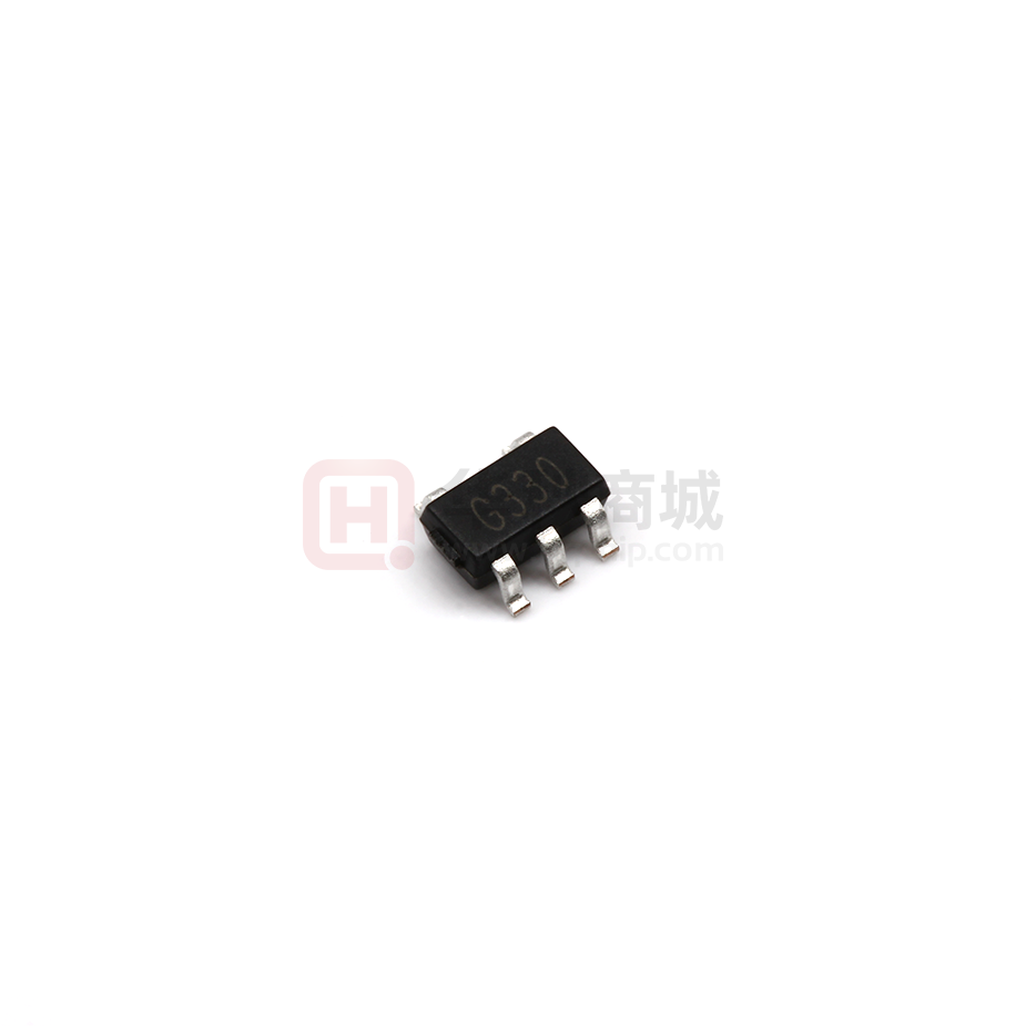
LM8805SF5-3.3
600mA, Fixed
G33Y
Reel
Active
SOT-89 3L
LM8805F-3.3
600mA, Fixed
8805 3.3 Yww
Reel
Active
VOUT
Package
Order No.
Description
ADJ
SOT-23 5L
LM8805SF5-ADJ
SOT-23 5L
1.2 V
1.8V
2.5 V
3.3 V
LM 8805
Output Voltage : ADJ / 1.2V / 1.8V / 2.5V / 3.3V
Package Type
: SOT-23 5L
SF5
F
: SOT-89
Root Name
Product Code
PIN CONFIGURATION
VOUT
BYP/ADJ
5
4
1
VIN
2
3
1
2
3
GND
EN
GND
VIN
VOUT
SOT-23 5L
SOT-89 3L
PIN DESCRIPTION
SOT-23 5L
Pin No.
SOT-89 3L
Name
Function
Name
Function
1
VIN
Input Supply
GND
Ground
2
GND
Ground
VIN
Input Supply
3
EN
Enable
VOUT
Output Voltage
4
BYP/ADJ
Bypass for Fixed output or
Output adjust for Adjustable output
-
-
5
VOUT
Output Voltage
-
-
Feb. 2017 - Rev. 1.8.2
-2
-
HTC
�600mA CMOS L.D.O. Regulator
LM8805
TYPICAL APPLICATION
Typical 3 Pin Application Circuit
VIN
VIN
VOUT
VOUT
LM8805-X.X
CIN
COUT
GND
Typical 5 Pin Application Circuit
- Output Adjustment (Adjustable version)
VIN
VIN
VOUT
VOUT
LM8805-ADJ
R2
CIN
EN
GND
COUT
ADJ
R1
- Fixed Voltage Application
VIN
VIN
VOUT
VOUT
LM8805-X.X
CIN
EN
COUT
GND BYP*
CBYP
(Optional)
* Note) BYP pin can be left open if low noise operation is not required.
Feb. 2017 - Rev. 1.8.2
-3
-
HTC
�600mA CMOS L.D.O. Regulator
LM8805
ELECTRICAL CHARACTERISTICS
(At TA =25℃, VIN = VOUT(nominal) + 1V, unless otherwise noted)
PARAMETER
Output Voltage Accuracy
Adjustable Voltage
line Regulation
Load Regulation
(Note 1)
Dropout Voltage
Maximum Output Current
Current Limit
SYMBOL
TEST CONDITION
+1.5
+2
%
VADJ
IO = 1mA
IO = 1 to 600mA
1.251
1.232
1.27
1.289
1.295
V
-0.3
0.05
0.3
%/V
%
ΔVLINE
IO = 1mA, (VOUT+1V) 0.96*VRating
600
ICL
VEN = GND
EN Input Low Current
VEN = VIN
EN Supply Current
VEN = VIN
-1
VIN = 2.5 to 5.5V
EN Input Threshold High
VIH
VIN = 2.5 to 5.5V
IGND
IOUT = 0mA to 600mA
IGND_OFF
1300
mA
600
usec
-0.3
0.01
VIL
VEN = 0V
nA
uA
1
uA
0.4
V
2
-
mV
mA
100
EN Input Threshold Low
V
50
85
uA
-
1
uA
TSD
IOUT = 10mA
155
℃
ΔTSD
IOUT = 10mA
10
℃
IOUT = 10mA
30
ppm
IOUT = 100mA, COUT = 2.2uF,
f = 100Hz
55
dB
VO Temperature Coefficient
Power Supply Ripple Rejection
UNIT
-1.5
-3
EN Input Bias Current
Thermal Shutdown Hysterisis
MAX.
IO = 1mA
IO = 1 to 600mA
CBP = 0uF, COUT = 1uF
IO = 100mA
Thermal Shutdown Temperature
TYP.
VO
EN Exit Delay
Ground Pin Current
MIN.
PSRR
Note 1. Load Regulation is measured using pulse techniques with duty cycle < 5%
Feb. 2017 - Rev. 1.8.2
-4
-
HTC
�600mA CMOS L.D.O. Regulator
LM8805
TYPICAL OPERATING CHARACTERISTICS
- VIN = 3.3V, VOUT = 2.5V
Vin
Vin
Vout
Vout
VIN : 1.0V/div, VOUT : 1.0V/div, Time : 10ms/div
VIN : 1.0V/div, VOUT : 1.0V/div, Time : 10ms/div
Start Up @ Iout=0.3A
Start Up @ Iout=0.6A
(Cin=10uF, Cout=10uF, R2=36KΩ, R1=35KΩ)
(Cin=10uF, Cout=10uF, R2=36KΩ, R1=35KΩ)
Vout
Vout
Iout
Iout
VOUT : 50mV/div, IOUT : 0.2A/div, Time : 50ms/div
VOUT : 50mV/div, IOUT : 0.2A/div, Time : 50ms/div
Load Transient Response
Load Transient Response
(Cin=10uF, Cout=10uF, R2=36KΩ, R1=35KΩ)
(Cin=10uF, Cout=10uF, R2=36KΩ, R1=35KΩ)
Vin
Vin
Ven
Ven
Vout
Vout
VIN : 2.0V/div, VEN : 2.0V, VOUT : 2.0V/div, Time : 1m/div
VIN : 2.0V/div, VEN : 2.0V, VOUT : 2.0V/div, Time : 1ms/div
Start Up by external VEN @ Iout=0A
Start Up by external VEN @ Iout=0.6A
(Cin=10uF, Cout=10uF, R2=36KΩ, R1=35KΩ)
(Cin=10uF, Cout=10uF, R2=36KΩ, R1=35KΩ)
Feb. 2017 - Rev. 1.8.2
-5
-
HTC
�600mA CMOS L.D.O. Regulator
LM8805
Max. VDROP.
Iout=0mA
Iout=10mA
Typ. VDROP
Dropout Voltage @ Vout=3.3V
Ground Currnet @ Iout=0A / 10mA
(Cin=10uF, Cout=10uF, R2=36KΩ, R1=35KΩ))
Feb. 2017 - Rev. 1.8.2
-6
-
HTC
�600mA CMOS L.D.O. Regulator
LM8805
APPLICATION INFORMATION
Detailed Description
The LM8805 consists of a high-precision voltage reference, an error correction circuit, and a current limited
output driver. With good transient responses, output remains stable even during load changes. The SHDN
input enables the output to be turned off, resulting in reduced power consumption.
The LM8805 incorporates both over-temperature and over-current protection.
External Capacitors
The LM8805 can stable work with cheap MLCC output Capacitor.
The LM8805 having high ripple rejection ratios, the series can be used with power supply noise. A 470pF
capacitor from the Bypass input to ground reduces noise present on the internal reference, which in turn
significantly reduces output noise. If output noise is not a concern, this input may be left unconnected. Larger
capacitor values Cbp be used, but results in a longer time period to rated output voltage when power is initially
applied.
Output Adjustment (Adjustable Version)
The operating condition of VIN and the operating characteristics of VOUT depend on the dropout voltage
performance in accordance with output load current.
VIN
VIN
VOUT
VOUT
LM8805-ADJ
R2
CIN
EN
GND
COUT
ADJ
R1
VOUT = VADJ(1+R2/R1)
Maximum Output Current Capability
The LM8805 can deliver a continuous current of 600mA over the full operating junction temperature range.
However, the output current is limited by the restriction of power dissipation which differs from packages.
A heat sink may be required depending on the maximum power dissipation and maximum ambient
temperature of application. With respect to the applied package, the maximum output current of 600mA
may be still undeliverable due to the restriction of the power dissipation of LM8805. Under all possible
conditions, the junction temperature must be within the range specified under operating conditions.
The temperatures over the device are given by:
Feb. 2017 - Rev. 1.8.2
-7
-
HTC
�600mA CMOS L.D.O. Regulator
LM8805
TC = TA + PD X θCA
TJ = TC + PD X θJC
TJ = TA + PD X θJA
where TJ is the junction temperature, T C is the case temperature, T A is the ambient temperature, PD is the
total power dissipation of the device, θCA is the thermal resistance of case-to-ambient, θJC is the thermal
resistance of junction-to-case, and θJA is the thermal resistance of junction to ambient.
The total power dissipation of the device is given by:
PD = PIN – POUT = (VIN X IIN)–(VOUT X IOUT)
= (VIN X (IOUT+IGND)) – (VOUT X IOUT) = (VIN - VOUT) X IOUT + VIN X IGND
where IGND is the operating ground current of the device which is specified at the Electrical Characteristics.
The maximum allowable temperature rise (T Rmax) depends on the maximum ambient temperature (T Amax) of
the application, and the maximum allowable junction temperature (T Jmax):
TRmax = TJmax – TAmax
The maximum allowable value for junction-to-ambient thermal resistance, θJA, can be calculated using the
formula:
θJA = TRmax / PD
Feb. 2017 - Rev. 1.8.2
-8
-
HTC
�600mA CMOS L.D.O. Regulator
LM8805
REVISION NOTICE
The description in this data sheet can be revised without any notice to describe its electrical characteristics
properly.
Feb. 2017 - Rev. 1.8.2
-9
-
HTC
�


 工商网监
湘ICP备2023018690号
工商网监
湘ICP备2023018690号
