DC-DC Converter Control Circuits
TJ34063A
FEATURES
Output Switch Current In Excess of 1.5A
2% Reference Accuracy
Low Quiescent Current : 2.5mA(Typ.)
Operating From 3V to 40V
Frequency Operation to 100KHz
Active Current Limiting
Moisture Sensitivity Level 3 for SMD Package
TJ34063AG is Halogen Free Products
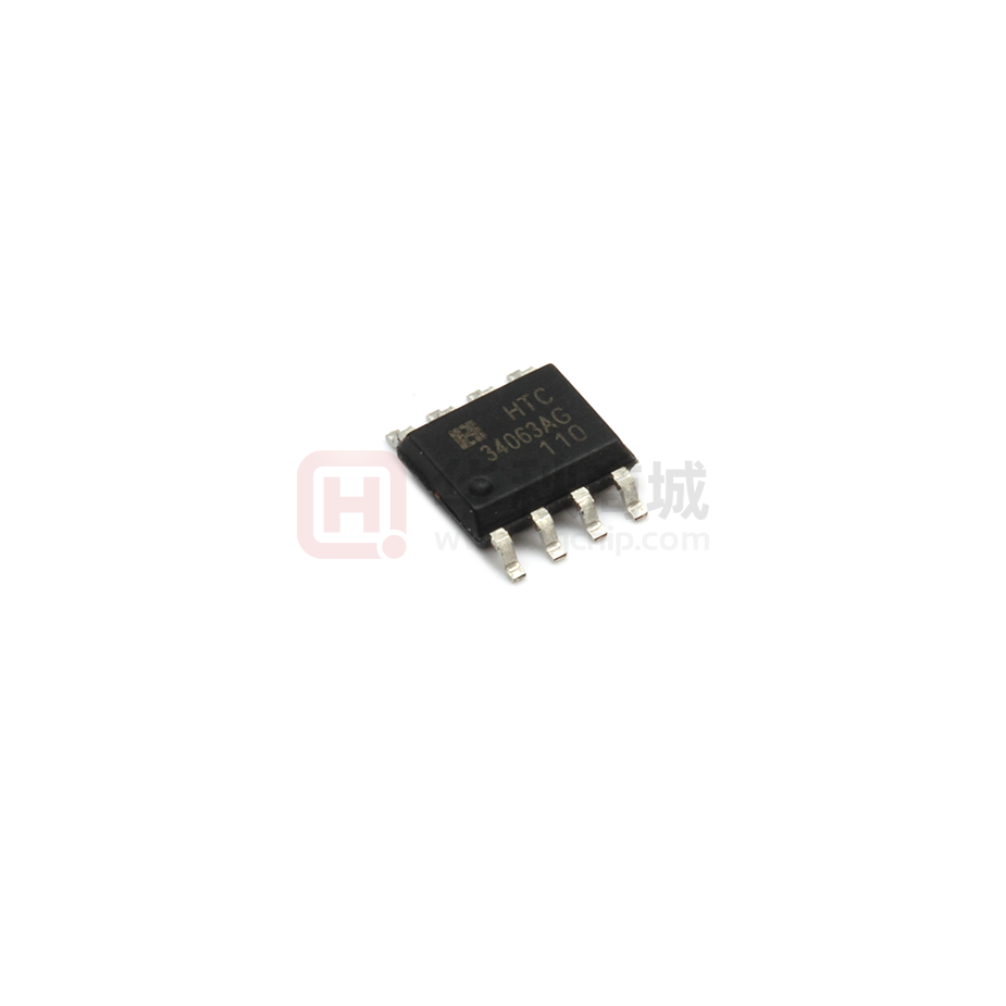
SOP-8 PKG
APPLICATION
Battery Chargers
ORDERING INFORMATION
NICs / Switches / Hubs
Device
Package
ADSL Modems
Negative Voltage Power Supplies
TJ34063AGD
SOP-8
DESCRIPTION
The TJ34063A series is a monolithic control circuit delivering the main functions for DC-DC voltage converting.
The device contains an internal temperature compensated reference, comparator, duty cycle controlled
oscillator with an active current limit circuit driver and high current output switch.
Output voltage is adjustable through two external resistors with a 2% reference accuracy.
Employing a minimum number of external components the TJ34063A devices series is designed for StepDown, Step-Up and Voltage-Inverting applications.
ABSOLUTE MAXIMUM RATINGS (Note 1)
CHARACTERISTIC
SYMBOL
MIN.
MAX.
UNIT
Power Supply Voltage
VCC
-
40
V
Comparator Input Voltage Range
VIR
-0.3
40
V
Switch Collector Voltage
VSWC
40
V
Switch Emitter Voltage(VSWC=40V)
VSWE
40
V
Switch Collector to Emitter Voltage
VCE
40
V
Driver Collector Voltage
Vdc
-
40
V
Idc
-
100
mA
ISW
-
1.5
A
Driver Collector Current
Switch Current
Jul. 2018 - Rev. 0.1
(Note 2)
-1-
HTC
�DC-DC Converter Control Circuits
TJ34063A
ABSOLUTE MAXIMUM RATINGS (Continued)
CHARACTERISTIC
SYMBOL
MIN.
MAX.
UNIT
Power Dissipation (at TA = 25°C)
SOP-8
PDMAX_SOP-8
0.76
W
Thermal Resistance(*)
SOP-8
θJA-SOP-8
130
°C/W
Operating Junction Temperature Range
Storage Temperature Range
TJ
-40
150
°C
TSTG
-65
150
°C
Note 1. Absolute Maximum Ratings are those values beyond which damage to the device may occur. Functional operation under these
conditions is not implied.
(*) This value depends from thermal design of PCB on which the device is mounted.
RECOMMENDED OPERATING CONDITIONS
CHARACTERISTIC
SYMBOL
MIN.
MAX.
UNIT
Supply Voltage
VCC
3
40
V
Operating Ambient Temperature
TA
-40
125
°C
ORDERING INFORMATION
Package
SOP-8
Order No.
TJ34063AGD
Description
1.5A, 100kHz
Supplied As
Status
Reel
Active
TJ 34063
Package Type
D : SOP-8
Green Mode
G : Halogen Free
Temperature Range
A : -40℃~125℃
Root Name
Product Code
Jul. 2018 - Rev. 0.1
-2-
HTC
�DC-DC Converter Control Circuits
TJ34063A
PIN CONFIGURATION
1
8
2
7
3
6
4
5
SOP-8
PIN DESCRIPTION
SOP-8 PKG
Pin No.
Name
Function
1
Switch Collector
Internal switch transistor collector
2
Switch Emitter
Internal switch transistor emitter
3
Timing Capacitor
Timing Capacitor to control the switching frequency
4
GND
Ground pin for all internal circuits
5
Comparator Inverting Input
Inverting input pin for internal comparator
6
VCC
Voltage supply
7
IPK Sense
8
Driver Collector
Peak Current Sense Input by monitoring the voltage drop across an
external I sense resistor to limit the peak current through the switch
Voltage driver collector
BLOCK DIAGRAM
Driver
Collector
8
S
1
Switch
Collector
2
Switch
Emitter
IPK
Oscillator
3
Timing
Capacitor
1.25V
Reference
Regulator
4
GND
Q
R
IPK Sense
VCC
Jul. 2018 - Rev. 0.1
Q1
7
6
Comparator
+
Comparator
Inverting
Input
Q2
5
-3-
HTC
�DC-DC Converter Control Circuits
TJ34063A
ELECTRICAL CHARACTERISTICS
(Refer to the test circuits, VCC=5V, TA=TLOW to THIGH, unless otherwise specified, see note 2)
SYMBOL
PARAMETER
TEST CONDITIONS
MIN.
TYP.
MAX.
UNIT
OSCILLATOR
FOSC
Frequency
VPIN5=0V, CT=1nF, TA=25℃
24
33
42
KHz
ICHG
Charge Current
VCC=5 to 40V, TA=25℃
24
35
42
㎂
Discharge Current
VCC=5 to 40V, TA=25℃
140
220
260
㎂
IDISCHG/ICHG
Discharge to Charge Current Ratio
Pin 7= VCC, TA=25℃
5.2
6.5
7.5
VIPK(SENSE)
Current Limit Sense Voltage
ICHG=IDISCHG, TA=25℃
250
300
350
mV
IDISCHG
OUTPUT SWITCH
VCE(SAT)
Saturation Voltage,
Darlington connection
ISW=1A, Pins 1,8 connected
1.0
1.3
V
VCE(SAT)
Saturation Voltage
ISW=1A, RPIN8=82Ω to VCC,
Forced β ~ 20
0.45
0.7
V
DC Current Gain
ISW=1A, VCE=5V, TA=25℃
Collector Off-State Current
VCE= 40V
1.0
100
㎂
1.25
1.275
V
1.29
V
hFE
IC(OFF)
50
75
COMPARATOR
VTH
REGLINE
IIB
TA=25℃
1.225
TA=TLOW to THIGH
1.21
Threshold Voltage
Threshold Voltage Line Regulation
VCC= 3 to 40V
1.4
5
mV
Input Bias Current
VIN= 0V
-20
-400
nA
VCC= 5 to 40V, CT=1nF
Pin7= VCC, VPIN5>VTH, Pin2=GND
Remaining pins open
1.4
4
mA
TOTAL DEVICE
ICC
Supply Current
Note 1. Maximum package power dissipation limit must be observed.
Note 2. TLOW= '-40℃, THIGH= '+125℃
Note 3. If Darlington configuration is not used, care must be taken to avoid deep saturation of output switch.
The resulting switch-off time may be adversely affected.
In a Darlington configuration the following output driver condition is suggested:
Forced β of output switch :
Ι C(OUTPUT)
Ι C(DRIVER) - 7.0mΑ *
≥10
* Currentless due to a built in 1KΩ anti-leakage resistor
Jul. 2018 - Rev. 0.1
-4-
HTC
�DC-DC Converter Control Circuits
TJ34063A
TYPICAL ELECTRICAL CHARACTERISTICS
Emitter Follower Configuration Output
Output Switch ON-OFF Time
Saturation Voltage vs. Emitter Current
vs. Oscillator Timing Capacitor
Common Emitter Configuration Output Switch
Current Limit Sense Voltage (VIPK)
Saturation Voltage vs. Collector Current
vs. Temperature
Standby supply current vs. Supply voltage
Jul. 2018 - Rev. 0.1
-5-
HTC
�DC-DC Converter Control Circuits
TJ34063A
TYPICAL APPLICATION CIRCUIT
Step-Up Converter
L1
170uH
R3
180Ω
8
1
DRC
SWC
IPK
SWE
7
RSC
0.22Ω
2
6
VCC
TC
5
12V
4
CII
VIN
D1
1N5819
3
GND
VOUT
C3
1.5nF
+
C2
100uF
28V / 175mA
TJ34063A
R1
2.2kΩ
+
R2
47kΩ
C1
330uF
Step-Down Converter
8
1
DRC
SWC
7
RSC
0.33Ω
IPK
SWE
6
3
VCC
TC
5
25V
C2
100uF
Jul. 2018 - Rev. 0.1
GND
+
R1
1.2kΩ
L1
220uH
4
CII
VIN
D1
1N5819
2
C3
470pF
+
R2
3.6kΩ
-6-
VOUT
C1
470uF
5V / 0.5A
HTC
�DC-DC Converter Control Circuits
TJ34063A
Step-Up with External NPN Switch
8
S
Q
R
VOUT
1
Q2
+
Q1
2
7
RSC
VIN
IPK
Oscillator
3
1.25V
Reference
Regulator
4
6
Comparator
+
5
Voltage Inverting Converter
8
1
DRC
SWC
IPK
SWE
7
RSC
0.24Ω
2
6
3
VCC
TC
5
VIN
4.5V to 6V
D1
1N5819
4
CII
C2
100uF
L1
88uH
GND
+
C3
1.5nF
VOUT
R1
8.2kΩ
Jul. 2018 - Rev. 0.1
R2
953Ω
C1
1000uF
-7-
+
-12V / 100mA
HTC
�DC-DC Converter Control Circuits
TJ34063A
Step-Down with External PNP Switch
8
S
Q
1
Q2
R
Q1
VOUT
+
2
7
RSC
VIN
IPK
Oscillator
3
1.25V
Reference
Regulator
4
6
Comparator
+
5
Voltage Inverting with External NPN Switch
8
S
Q
1
Q2
R
Q1
2
7
RSC
VIN
IPK
Oscillator
3
1.25V
Reference
Regulator
4
VOUT
6
Comparator
+
-
+
5
Jul. 2018 - Rev. 0.1
-8-
HTC
�DC-DC Converter Control Circuits
TJ34063A
REVISION NOTICE
The description in this data sheet can be revised without any notice to describe its electrical characteristic properly.
Jul. 2018 - Rev. 0.1
-9-
HTC
�
很抱歉,暂时无法提供与“TJ34063AGD”相匹配的价格&库存,您可以联系我们找货
免费人工找货- 国内价格
- 1+0.83999
- 30+0.80999
- 100+0.77999
- 500+0.72000
- 1000+0.69000
- 2000+0.67200


 工商网监
湘ICP备2023018690号
工商网监
湘ICP备2023018690号

