DATASHEET
EL5173, EL5373
FN7312
Rev 10.00
August 25, 2015
450MHz Differential Twisted-Pair Drivers
The EL5173 and EL5373 are single and triple high bandwidth
amplifiers with a fixed gain of 2. They are primarily targeted for
applications such as driving twisted-pair lines in component video
applications. The inputs can be in either single-ended or
differential form but the outputs are always in differential form.
Features
The output common mode level for each channel is set by the
associated REF pin, which has a -3dB bandwidth of over
190MHz. Generally, these pins are grounded but can be tied to
any voltage reference.
• 900V/µs slew rate (EL5173)
All outputs are short circuit protected to withstand temporary
overload condition.
• 40mA maximum output current
The EL5173 and EL5373 are specified for operation over the
full -40°C to +85°C temperature range.
• Pb-free available (RoHS compliant)
• Fully differential inputs and outputs
• Differential input range ±2.3V
• 450MHz 3dB bandwidth at fixed gain of 2
• 1100V/µs slew rate (EL5373)
• Single 5V or dual ±5V supplies
• Low power - 12mA per channel
Applications
• Twisted-pair drivers
• Differential line drivers
• VGA over twisted-pairs
• ADSL/HDSL drivers
• Single-ended to differential amplification
• Transmission of analog signals in a noisy environment
Pinouts
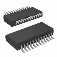
EL5373
(24 LD QSOP)
TOP VIEW
EL5173
(8 LD SOIC, MSOP)
TOP VIEW
1 IN+
OUT 8
EN 1
2 EN
VS- 7
INP1 2
3 IN-
VS+ 6
INN1 3
22 NC
OUTB 5
REF1 4
21 VSP
NC 5
20 VSN
4 REF
+
-
INN2 7
+
-
REF2 8
REF3 12
FN7312 Rev 10.00
August 25, 2015
18 OUT2
17 OUT2B
16 NC
NC 9
INN3 11
23 OUT1B
19 NC
INP2 6
INP3 10
24 OUT1
+
-
15 OUT3
14 OUT3B
13 NC
Page 1 of 15
�EL5173, EL5373
Pin Descriptions
EL5173
EL5373
PIN NUMBER
PIN NAME
PIN NUMBER
PIN NAME
PIN FUNCTION
1
IN+
2, 6, 10
INP1,
INP2, INP3
2
EN
1
EN
3
IN-
3, 7, 11
INN1, INN2, INN3
Inverting inputs, note that on EL5173, this pin is also the
REF pin
4
REF
4, 8, 12
REF1, REF2, REF3
Reference inputs, sets common-mode output voltage
5
OUTB
14, 17, 23
OUT3B, OUT2B, OUT1B
6
VS+
21
VSP
Positive supply
7
VS-
20
VSN
Negative supply
8
OUT
15, 18, 24
OUT3, OUT2, OUT1
-
NC
5, 9, 13, 16, 19, 22
NC
Non-inverting inputs
ENABLE
Inverting outputs
Non-inverting outputs
No connect; grounded for best crosstalk performance
Ordering Information
PART NUMBER
(Notes 1, 2, 3)
EL5173ISZ
PART
MARKING
5173ISZ
PACKAGE
(RoHS Compliant)
PKG.
DWG. #
8 Ld SOIC
M8.15E
EL5173IYZ (No longer available,
BAAYA
recommended replacement: EL5173ISZ)
8 Ld MSOP
M8.118A
EL5373IUZ
24 Ld QSOP
MDP0040
EL5373IUZ
NOTES:
1. Add “-T*” suffix for tape and reel. Please refer to TB347 for details on reel specifications.
2. These Intersil Pb-free plastic packaged products employ special Pb-free material sets, molding compounds/die attach materials, and 100% matte
tin plate plus anneal (e3 termination finish, which is RoHS compliant and compatible with both SnPb and Pb-free soldering operations). Intersil
Pb-free products are MSL classified at Pb-free peak reflow temperatures that meet or exceed the Pb-free requirements of IPC/JEDEC J STD-020.
3. For Moisture Sensitivity Level (MSL), please see device information page for EL5173, EL5373. For more information on MSL please see tech brief
TB363.
FN7312 Rev 10.00
August 25, 2015
Page 2 of 15
�EL5173, EL5373
Absolute Maximum Ratings (TA = +25°C)
Thermal Information
Supply Voltage (VS+ to VS-) . . . . . . . . . . . . . . . . . . . . . . . . . . . . . . . . . . 12.6V
Supply Voltage Slew Rate . . . . . . . . . . . . . . . . . . . . . . . . . . . . . . .1V/µs max.
Supply Voltage Rate-of-rise (dV/dT) . . . . . . . . . . . . . . . . . . . . . . . . . . . 1V/µs
Input Voltage (IN+, IN- to VS+, VS-) . . . . . . . . . . . . . VS- - 0.3V to VS+ + 0.3V
Differential Input Voltage (IN+ to IN-). . . . . . . . . . . . . . . . . . . . . . . . . . ±4.8V
Maximum Output Current . . . . . . . . . . . . . . . . . . . . . . . . . . . . . . . . . . ±60mA
Operating Junction Temperature . . . . . . . . . . . . . . . . . . . . . . . . . . . .+135°C
Recommended Operating Temperature . . . . . . . . . . . . . . . -40°C to +85°C
Storage Temperature Range. . . . . . . . . . . . . . . . . . . . . . . .-65°C to +150°C
Power Dissipation. . . . . . . . . . . . . . . . . . . . . . . . . . . . . . . . . . . . . . See Curves
Pb-Free Reflow Profile . . . . . . . . . . . . . . . . . . . . . . . . . . . . . . . see link below
http://www.intersil.com/pbfree/Pb-FreeReflow.asp
CAUTION: Do not operate at or near the maximum ratings listed for extended periods of time. Exposure to such conditions may adversely impact product
reliability and result in failures not covered by warranty.
IMPORTANT NOTE: All parameters having Min/Max specifications are guaranteed. Typ values are for information purposes only. Unless otherwise noted, all tests are
at the specified temperature and are pulsed tests, therefore: TJ = TC = TA
Electrical Specifications
PARAMETER
VS+ = +5V, VS- = -5V, TA = +25°C, VIN = 0V, RLD = 200, CLD = 1pF, Unless Otherwise Specified.
DESCRIPTION
CONDITIONS
MIN
(Note 4)
TYP
MAX
(Note 4)
UNIT
AC PERFORMANCE
BW
-3dB Bandwidth
450
MHz
BW
±0.1dB Bandwidth
60
MHz
SR
Slew Rate - EL5173
VOUT = 2VP-P, 20% to 80%
750
900
V/µs
Slew Rate - EL5373
VOUT = 2VP-P, 20% to 80%
900
1100
V/µs
tSTL
Settling Time to 0.1%
VOUT = 2VP-P
10
ns
OS
Overshoot
VODP-P = 2V
10
%
tOVR
Output Overdrive Recovery Time
10
ns
VREFBW (-3dB)
VREF -3dB Bandwidth
AV =1, CLD = 2.7pF
190
MHz
VREFSR+
VREF Slew Rate - Rise
VOUT = 2VP-P, 20% to 80%
200
V/µs
VREFSR-
VREF Slew Rate - Fall
VOUT = 2VP-P, 20% to 80%
125
V/µs
VN
Input Voltage Noise
f = 10kHz
25
nV/Hz
HD2
Second Harmonic Distortion
VOUT = 2VP-P, 5MHz
84
dBc
HD2
Second Harmonic Distortion
VOUT = 2VP-P, 20MHz
71
dBc
HD3
Third Harmonic Distortion
VOUT = 2VP-P, 5MHz
62
dBc
HD3
Third Harmonic Distortion
VOUT = 2VP-P, 20MHz
53
dBc
dG
Differential Gain at 3.58MHz
RLD = 300, AV = 2
0.05
%
d
Differential Phase at 3.58MHz
RLD = 300, AV = 2
0.08
°
eS
Channel Separation - for EL5373 only
at 1MHz
90
dB
INPUT CHARACTERISTICS
VOS
Input Referred Offset Voltage
IIN
Input Bias Current (VIN, VINB)
IREF
INput Bias Current at REF
Gain
Gain Accuracy
RIN
Differential Input Resistance
CIN
Differential Input Capacitance
DMIR
Differential Mode Input Range
FN7312 Rev 10.00
August 25, 2015
±3
±30
mV
EL5173
-21
-11
-5
µA
EL5373
-21
-13
-5
µA
VREF = +3.2V
1
5
µA
VREF = -3.2V
-1
+1
µA
2.01
V
VIN = ±1V
1.97
±2
1.99
150
k
1
pF
±2.3
V
Page 3 of 15
�EL5173, EL5373
Electrical Specifications
PARAMETER
VS+ = +5V, VS- = -5V, TA = +25°C, VIN = 0V, RLD = 200, CLD = 1pF, Unless Otherwise Specified. (Continued)
DESCRIPTION
CONDITIONS
CMIR+
Common Mode Positive Input Range at
VIN+, VIN-
CMIR-
Common Mode Negative Input Range at
VIN+, VIN-
VREFIN+
Reference Input - Positive
VIN+ = VIN- = 0V
VREFIN-
Reference Input - Negative
VIN+ = VIN- = 0V
VREFOS
Output Offset Relative to VREF
CMRR
Input Common Mode Rejection Ratio
MIN
(Note 4)
TYP
3.1
3.4
-4.5
3.3
MAX
(Note 4)
UNIT
V
-4.2
3.7
V
V
-3.3
-3
V
-100
50
+100
mV
VIN = ±2.5V
60
80
dB
RLD = 200
3.3
3.67
V
OUTPUT CHARACTERISTICS
VOUT
(EL5173)
Positive Output Voltage Swing
VOUT
(EL5373)
Positive Output Voltage Swing
IOUT(Max)
Maximum Output Current
ROUT
Negative Output Voltage Swing
-3.3
RLD = 200
3.7
Negative Output Voltage Swing
-3
4
-3.7
V
V
-3.4
V
RL = 10(EL5173)
±45
±55
mA
RL = 10(EL5373)
±40
±50
mA
60
m
Output Impedance
SUPPLY
VSUPPLY
Supply Operating Range
IS(ON)
Power Supply Current - Per Channel
IS(OFF)+ (EL5173)
Positive Power Supply Current - Disabled
IS(OFF)- (EL5173)
Negative Power Supply Current - Disabled
IS(OFF)+ (EL5373)
Positive Power Supply Current - Disabled
IS(OFF)- (EL5373)
Negative Power Supply Current - Disabled
PSRR
Power Supply Rejection Ratio
VS+ to VS-
EN pin tied to 4.8V
EN pin tied to 4.8V
VS from ±4.5V to ±5.5V
4.75
11
V
9
12
14
mA
60
80
100
µA
-150
-120
-90
µA
0.5
2
10
µA
-150
-120
-90
µA
60
73
dB
ENABLE
tEN
Enable Time
100
ns
tDS
Disable Time
1.2
µs
VIH
EN Pin Voltage for Power-Up
VIL
EN Pin Voltage for Shut-Down
IIH-EN
EN Pin Input Current High - Per Channel
At VEN = 5V
IIL-EN
EN Pin Input Current Low - Per Channel
At VEN = 0V
VS+ - 1.5
VS+ - 0.5
V
40
-5
V
-2.5
60
µA
µA
NOTE:
4. Parameters with MIN and/or MAX limits are 100% tested at +25°C, unless otherwise specified. Temperature limits established by characterization
and are not production tested.
FN7312 Rev 10.00
August 25, 2015
Page 4 of 15
�EL5173, EL5373
FN7312 Rev 10.00
August 25, 2015
Connection Diagrams
CL1
RS1
50
-5V
RRT2
1 IN+
OUT 8
EN
2 EN
VS- 7
INN
3 IN-
VS+ 6
REF
4 REF
INP
RS2
50
LOADP
50
RRT2
OUTB 5
RS3
50
+5V
CL2
LOADN
50
FIGURE 1. EL5173
+5V
ENABLE
1 EN
INP1
2 INP1
RRT1
OUT1 24
RRT1B
OUT1B 23
LD1
50
LD1B
50
INN1
3 INN1
NC 22
REF1
4 REF1
VSP 21
5 NC
VSN 20
INP2
6 INP2
NC 19
INN2
7 INN2
OUT2 18
RRT2
RRT2B
REF2
8 REF2
OUT2B 17
10 INP3
Page 5 of 15
11 INN3
OUT3B 14
REF3
12 REF3
NC 13
RSN1
50
RSR1
50
RSP2
50
RSN2
50
RSR2
50
RSP3
50
RSN3
50
RRT3
OUT3 15
INN3
RSP1
50
LD2B
50
NC 16
9 NC
INP3
LD2
50
RRT3B
50
RSR3
50
-5V
FIGURE 2. EL5373
LD3
50
LD3B
�EL5173, EL5373
Typical Performance Curves
VS = ±5V, CLD = 1pF
VS = ±5V, RLD = 200
10
10
9
9
8
8
RLD = 500
7
VODP-P = 200mV
6
GAIN (dB)
GAIN (dB)
7
RLD = 1k
5
4
3
6
5
RLD = 200
4
3
VODP-P = 700mV
2
RLD = 100
2
1
1
0
1M
10M
100M
0
100k
1G
100M
1G
FREQUENCY (Hz)
FIGURE 4. FREQUENCY RESPONSE vs RLD
FIGURE 3. FREQUENCY RESPONSE
VS = ±5V, RLD = 200, VODP-P = 200mV
5
11
4
10
CLD = 16pF
8
3
GAIN (dB)
9
GAIN (dB)
10M
1M
FREQUENCY (Hz)
CLD = 5pF
7
6
4
0
-2
CLD = 0pF
3
-3
2
-4
1
1M
10M
VREF = 200mVP-P
1
-1
CLD = 2.3pF
5
2
100M
VREF = 1VP-P
-5
1M
1G
10M
100M
1G
FREQUENCY (Hz)
FREQUENCY (Hz)
FIGURE 6. FREQUENCY RESPONSE vs VREF
FIGURE 5. SMALL SIGNAL FREQUENCY RESPONSE vs CLD
100
VINCM
+
-
VODM
VOCM
100
COMMON MODE REJECTION (dB)
0
-10
-20
PSRR (dB)
-30
PSRR-
-40
-50
-60
PSRR+
-70
-80
-90
100k
1M
10M
FREQUENCY (Hz)
FIGURE 7. PSRR vs FREQUENCY
FN7312 Rev 10.00
August 25, 2015
100M
0
-10
-20
-30
-40
VOCM/VINCM
-50
-60
-70
VODM/VINCM
-80
-90
100k
1M
10M
100M
1G
FREQUENCY (Hz)
FIGURE 8. COMMON MODE REJECTION vs FREQUENCY
Page 6 of 15
�EL5173, EL5373
Typical Performance Curves
(Continued)
100
VIN
+
-
RT
VOCM
VODM
R
100
1000
VOLTAGE NOISE (nV/Hz)
0
BALANCE ERROR (dB)
-10
-20
-30
-40
VOCM/VODM
-50
-60
100k
1M
10M
100M
100
10
10
1G
100
1k
10k
100k
1M
10M
FREQUENCY (Hz)
FREQUENCY (Hz)
FIGURE 10. INPUT VOLTAGE NOISE vs FREQUENCY
FIGURE 9. DIFFERENTIAL MODE OUTPUT BALANCE ERROR vs
FREQUENCY
460
-40
440
420
-50
CH3 --> CH2
CH2 --> CH1
-60
-70
BW (MHz)
CHANNEL SEPARATION (dB)
VODMP-P = 200mV, RLD = 200
-30
CH2 --> CH3
-80
CH1 --> CH2
-90
400
380
360
340
CH3 --> CH1
-100
CH1 --> CH3
-110
100k
1M
10M
320
100M
1G
300
4
5
6
FIGURE 11. CHANNEL SEPARATION vs FREQUENCY
-40
VS = ±5V, RLD = 200
-45
11.8
HD3 (f = 20MHz)
-50
DISTORTION (dB)
IS+
11.7
IS (mA)
11
10
FIGURE 12. SMALL SIGNAL BANDWIDTH vs SUPPLY VOLTAGE
11.9
IS-
11.5
-55
HD3 (f = 5MHz)
-60
-65
-70
HD2 (f = 20MHz)
-75
HD2 (f = 5MHz)
-80
11.4
11.3
4
9
VS (V)
FREQUENCY (Hz)
11.6
8
7
-85
-90
5
6
8
7
9
10
11
VS (V)
FIGURE 13. SUPPLY CURRENT vs SUPPLY VOLTAGE
FN7312 Rev 10.00
August 25, 2015
1
2
3
4
5
6
7
8
9
DIFFERENTIAL OUTPUT VOLTAGE (V)
FIGURE 14. HARMONIC DISTORTION vs DIFFERENTIAL OUTPUT
VOLTAGE
Page 7 of 15
�EL5173, EL5373
Typical Performance Curves
-40
(Continued)
VS = ±5VVODMP-P = 2V
-40
VS = ±5V, RLD = 200, VODMP-P = 2V
-45
-50
-50
DISTORTION (dB)
DISTORTION (dB)
HD3 (f = 20MHz)
-60
HD3 (f
-70
= 5M Hz
)
HD2 (f = 20MHz)
-80
-90
200
300
400
500
600
700
-60
H D2
-65
-70
-75
-80
HD2 (f = 5MHz)
-100
100
HD3
-55
-85
800
900 1000
-90
0M
5M
10M
15M
20M
25M
30M
35M
40M
FREQUENCY (Hz)
RLD (W)
FIGURE 15. HARMONIC DISTORTION vs RLD
FIGURE 16. HARMONIC DISTORTION vs FREQUENCY
0.5V/DIV
100mV/DIV
20ns/DIV
20ns/DIV
FIGURE 17. SMALL SIGNAL TRANSIENT RESPONSE
FIGURE 18. LARGE SIGNAL TRANSIENT RESPONSE
EMPTY
BOARD
DISABLED
OUT1B
OUT1
FIGURE 19. OUTPUT IMPEDANCE (DISABLED)
FN7312 Rev 10.00
August 25, 2015
FIGURE 20. OUTPUT IMPEDANCE (ENABLED)
Page 8 of 15
�EL5173, EL5373
Typical Performance Curves
(Continued)
FIGURE 21. DISABLED RESPONSE
JEDEC JESD51-7 HIGH EFFECTIVE THERMAL
CONDUCTIVITY TEST BOARD
1.2
1.136W
1.2
1.0
909mW
0.8
870mW
POWER DISSIPATION (W)
POWER DISSIPATION (W)
1.4
FIGURE 22. ENABLED RESPONSE
QSOP24
JA = +88°C/W
SO8
JA = +110°C/W
0.6
MSOP8/10
JA = +115°C/W
0.4
0.2
0
0
25
75 85 100
50
125
1.0
870mW
0.8
QSOP24
JA = +115°C/W
625mW
0.6
SO8
JA = +160°C/W
0.4 486mW
MSOP8
JA = +206°C/W
0.2
0
150
JEDEC JESD51-3 LOW EFFECTIVE THERMAL
CONDUCTIVITY TEST BOARD
AMBIENT TEMPERATURE (°C)
0
25
50
75 85 100
125
150
AMBIENT TEMPERATURE (°C)
FIGURE 23. PACKAGE POWER DISSIPATION vs AMBIENT
TEMPERATURE
FIGURE 24. PACKAGE POWER DISSIPATION vs AMBIENT
TEMPERATURE
Simplified Schematic
200
VS+
R1
IN+
IN-
R3
R2
FBP
R4
R7
R8
FBN
VB1
OUT+
RCD
REF
RCD
OUT-
VB2
CC
R9
R10
CC
R5
R6
VS-
400
FN7312 Rev 10.00
August 25, 2015
200
Page 9 of 15
�EL5173, EL5373
Description of Operation and
Application Information
Product Description
The EL5173 and EL5373 are wide bandwidth, low power and
single/differential ended to differential output amplifiers. They
have a fixed gain of 2. The EL5173 is a single channel
differential amplifier. The EL5373 is a triple channel
differential amplifier. The EL5173 and EL5373 have a -3dB
bandwidth of 450MHz while driving a 200 differential load.
The EL5173 and EL5373 are available with a power-down
feature to reduce the power while the amplifiers are disabled.
Input, Output and Supply Voltage Range
The EL5173 and EL5373 have been designed to operate with a
single supply voltage of 5V to 10V or split supplies with its total
voltage from 5V to 10V. The amplifiers have an input common
mode voltage range from -4.5V to 3.4V for ±5V supply. The
differential mode input range (DMIR) between the two inputs
is from -2.3V to +2.3V. The input voltage range at the REF pin is
from -3.3V to 3.7V. If the input common mode or differential
mode signal is outside the above-specified ranges, it will cause
the output signal to become distorted.
The output of the EL5173 and EL5373 can swing from -3.3V to
3.6V at 200 differential load at ±5V supply. As the load
resistance becomes lower, the output swing is reduced.
logic signal is relative to VS+ pin. Letting the EN pin float or
applying a signal that is less than 1.5V below VS+ will enable
the amplifier. The amplifier will be disabled when the signal at
EN pin is above VS+ - 0.5V.
Output Drive Capability
The EL5173 and EL5373 have internal short circuit protection.
Its typical short circuit current is ±55mA. If the output is
shorted indefinitely, the power dissipation could easily
increase such that the part will be destroyed. Maximum
reliability is maintained if the output current never exceeds
±60mA. This limit is set by the design of the internal metal
interconnect.
Power Dissipation
With the high output drive capability of the EL5173 and EL5373,
it is possible to exceed the +125°C absolute maximum junction
temperature under certain load current conditions. Therefore, it
is important to calculate the maximum junction temperature for
the application to determine if the load conditions or package
types need to be modified for the amplifier to remain in the safe
operating area.
The maximum power dissipation allowed in a package is
determined according to Equation 1:
T JMAX – T AMAX
PD MAX = -------------------------------------------- JA
(EQ. 1)
Differential and Common Mode Gain
Settings
Where:
As shown in the “Simplified Schematic” on page 9, since the
feedback resistors RF and the gain resistor are integrated with
200 and 400, the EL5173 and EL5373 have a fixed gain of
2. The common mode gain is always one.
• TAMAX = Maximum ambient temperature
Driving Capacitive Loads and Cables
The EL5173 and EL5373 can drive 16pF differential capacitor
in parallel with 200 differential load with less than 3.5dB of
peaking. If less peaking is desired in applications, a small
series resistor (usually between 5 to 50) can be placed in
series with each output to eliminate most peaking. However,
this will reduce the gain slightly.
When used as a cable driver, double termination is always
recommended for reflection-free performance. For those
applications, a back-termination series resistor at the
amplifier’s output will isolate the amplifier from the cable and
allow extensive capacitive drive. However, other applications
may have high capacitive loads without a back-termination
resistor. Again, a small series resistor at the output can help to
reduce peaking.
Disable/Power-Down
The EL5173 and EL5373 can be disabled and placed their
outputs in a high impedance state. The turn-off time is about
1.2µs and the turn-on time is about 100ns. When disabled, the
amplifier’s supply current is reduced to 40µA for IS+ and
2.5µA for IS- typically, thereby effectively eliminating the power
consumption. The amplifier’s power-down can be controlled by
standard CMOS signal levels at the ENABLE pin. The applied
FN7312 Rev 10.00
August 25, 2015
• TJMAX = Maximum junction temperature
• JA = Thermal resistance of the package
The maximum power dissipation actually produced by an IC is
the total quiescent supply current times the total power supply
voltage, plus the power in the IC due to the load, or as
expressed in Equation 2:
V O
PD = i V STOT I SMAX + V STOT – V O ------------
R LD
(EQ. 2)
Where:
VSTOT = Total supply voltage = VS+ - VSISMAX = Maximum quiescent supply current per channel
VO = Maximum differential output voltage of the
application
RLD = Differential load resistance
ILOAD = Load current
i = Number of channels
By setting the two PDMAX equations equal to each other, we
can solve the output current and RLOAD to avoid the device
overheat.
Page 10 of 15
�EL5173, EL5373
Power Supply Bypassing and Printed Circuit
Board Layout
As with any high frequency device, a good printed circuit board
layout is necessary for optimum performance. Lead lengths
should be as short as possible. The power supply pin must be
well bypassed to reduce the risk of oscillation. For normal
single supply operation, where the VS- pin is connected to the
ground plane, a single 4.7µF tantalum capacitor in parallel
with a 0.1µF ceramic capacitor from VS+ to GND will suffice.
This same capacitor combination should be placed at each
supply pin to ground if split supplies are to be used. In this
case, the VS- pin becomes the negative supply rail.
For good AC performance, parasitic capacitance should be
kept to minimum. Use of wire-wound resistors should be
avoided because of their additional series inductance. Use of
sockets should also be avoided if possible. Sockets add
parasitic inductance and capacitance that can result in
compromised performance. Minimizing parasitic capacitance
at the amplifier’s inverting input pin is very important. The
feedback resistor should be placed very close to the inverting
input pin. Strip line design techniques are recommended for
the signal traces.
Typical Applications
0
50
50
EL5173/
EL5373
50
ZO = 100
50
VFB
VIN
VINB
EL5175/
EL5375
VOUT
VREF
FIGURE 25. TWISTED PAIR CABLE DRIVER
FN7312 Rev 10.00
August 25, 2015
Page 11 of 15
�EL5173, EL5373
Revision History
The revision history provided is for informational purposes only and is believed to be accurate, but not warranted. Please go to the web to make sure that
you have the latest revision.
DATE
REVISION
August 25, 2015
FN7312.10
CHANGE
- Ordering Information Table on page 2.
- Added Revision History and About Intersil sections.
About Intersil
Intersil Corporation is a leading provider of innovative power management and precision analog solutions. The company's products
address some of the largest markets within the industrial and infrastructure, mobile computing and high-end consumer markets.
For the most updated datasheet, application notes, related documentation and related parts, please see the respective product
information page found at www.intersil.com.
You may report errors or suggestions for improving this datasheet by visiting www.intersil.com/ask.
Reliability reports are also available from our website at www.intersil.com/support
FN7312 Rev 10.00
August 25, 2015
Page 12 of 15
�EL5173, EL5373
Package Outline Drawing
M8.15E
8 LEAD NARROW BODY SMALL OUTLINE PLASTIC PACKAGE
Rev 0, 08/09
4
4.90 ± 0.10
A
DETAIL "A"
0.22 ± 0.03
B
6.0 ± 0.20
3.90 ± 0.10
4
PIN NO.1
ID MARK
5
(0.35) x 45°
4° ± 4°
0.43 ± 0.076
1.27
0.25 M C A B
SIDE VIEW “B”
TOP VIEW
1.75 MAX
1.45 ± 0.1
0.25
GAUGE PLANE
C
SEATING PLANE
0.10 C
0.175 ± 0.075
SIDE VIEW “A
0.63 ±0.23
DETAIL "A"
(1.27)
(0.60)
NOTES:
(1.50)
(5.40)
1.
Dimensions are in millimeters.
Dimensions in ( ) for Reference Only.
2.
Dimensioning and tolerancing conform to AMSE Y14.5m-1994.
3.
Unless otherwise specified, tolerance : Decimal ± 0.05
4.
Dimension does not include interlead flash or protrusions.
Interlead flash or protrusions shall not exceed 0.25mm per side.
5.
The pin #1 identifier may be either a mold or mark feature.
6.
Reference to JEDEC MS-012.
TYPICAL RECOMMENDED LAND PATTERN
FN7312 Rev 10.00
August 25, 2015
Page 13 of 15
�EL5173, EL5373
Package Outline Drawing
M8.118A
8 LEAD MINI SMALL OUTLINE PLASTIC PACKAGE (MSOP)
Rev 0, 9/09
3.0±0.1
8
A
0.25
CAB
3.0±0.1
4.9±0.15
DETAIL "X"
1.10 Max
PIN# 1 ID
B
SIDE VIEW 2
1
0.18 ± 0.05
2
0.65 BSC
TOP VIEW
0.95 BSC
0.86±0.09
H
GAUGE
PLANE
C
0.25
SEATING PLANE
0.33 +0.07/ -0.08
0.08 C A B
0.10 ± 0.05
3°±3°
0.10 C
0.55 ± 0.15
DETAIL "X"
SIDE VIEW 1
5.80
NOTES:
4.40
3.00
1.
Dimensions are in millimeters.
2.
Dimensioning and tolerancing conform to JEDEC MO-187-AA
and AMSE Y14.5m-1994.
3.
Plastic or metal protrusions of 0.15mm max per side are not
included.
4.
Plastic interlead protrusions of 0.25mm max per side are not
included.
5.
Dimensions “D” and “E1” are measured at Datum Plane “H”.
6.
This replaces existing drawing # MDP0043 MSOP 8L.
0.65
0.40
1.40
TYPICAL RECOMMENDED LAND PATTERN
FN7312 Rev 10.00
August 25, 2015
Page 14 of 15
�EL5173, EL5373
Quarter Size Outline Plastic Packages Family (QSOP)
MDP0040
A
QUARTER SIZE OUTLINE PLASTIC PACKAGES FAMILY
D
(N/2)+1
N
INCHES
SYMBOL QSOP16 QSOP24 QSOP28 TOLERANCE NOTES
E
PIN #1
I.D. MARK
E1
1
(N/2)
B
0.010
C A B
e
H
C
SEATING
PLANE
0.007
0.004 C
b
C A B
A
0.068
0.068
0.068
Max.
-
A1
0.006
0.006
0.006
±0.002
-
A2
0.056
0.056
0.056
±0.004
-
b
0.010
0.010
0.010
±0.002
-
c
0.008
0.008
0.008
±0.001
-
D
0.193
0.341
0.390
±0.004
1, 3
E
0.236
0.236
0.236
±0.008
-
E1
0.154
0.154
0.154
±0.004
2, 3
e
0.025
0.025
0.025
Basic
-
L
0.025
0.025
0.025
±0.009
-
L1
0.041
0.041
0.041
Basic
-
N
16
24
28
Reference
Rev. F 2/07
NOTES:
L1
A
1. Plastic or metal protrusions of 0.006” maximum per side are not
included.
2. Plastic interlead protrusions of 0.010” maximum per side are not
included.
c
SEE DETAIL "X"
3. Dimensions “D” and “E1” are measured at Datum Plane “H”.
4. Dimensioning and tolerancing per ASME Y14.5M-1994.
0.010
A2
GAUGE
PLANE
L
A1
4°±4°
DETAIL X
© Copyright Intersil Americas LLC 2005-2015. All Rights Reserved.
All trademarks and registered trademarks are the property of their respective owners.
For additional products, see www.intersil.com/en/products.html
Intersil products are manufactured, assembled and tested utilizing ISO9001 quality systems as noted
in the quality certifications found at www.intersil.com/en/support/qualandreliability.html
Intersil products are sold by description only. Intersil may modify the circuit design and/or specifications of products at any time without notice, provided that such
modification does not, in Intersil's sole judgment, affect the form, fit or function of the product. Accordingly, the reader is cautioned to verify that datasheets are
current before placing orders. Information furnished by Intersil is believed to be accurate and reliable. However, no responsibility is assumed by Intersil or its
subsidiaries for its use; nor for any infringements of patents or other rights of third parties which may result from its use. No license is granted by implication or
otherwise under any patent or patent rights of Intersil or its subsidiaries.
For information regarding Intersil Corporation and its products, see www.intersil.com
FN7312 Rev 10.00
August 25, 2015
Page 15 of 15
�


 工商网监
湘ICP备2023018690号
工商网监
湘ICP备2023018690号
