DATASHEET
ISL6568
FN9187
Rev 5.00
Jan 12, 2012
Two-Phase Buck PWM Controller with Integrated MOSFET Drivers for VRM9,
VRM10, and AMD Hammer Applications
The ISL6568 two-phase PWM control IC provides a precision
voltage regulation system for advanced microprocessors. The
integration of power MOSFET drivers into the controller IC
marks a departure from the separate PWM controller and
driver configuration of previous multi-phase product families.
By reducing the number of external parts, this integration is
optimized for a cost and space saving power management
solution.
Outstanding features of this controller IC include
programmable VID codes compatible with Intel VRM9,VRM10,
as well as AMD Hammer microprocessors. A unity gain,
differential amplifier is provided for remote voltage sensing,
compensating for any potential difference between remote
and local grounds. The output voltage can also be positively or
negatively offset through the use of a single external resistor.
Features
• Integrated Multi-Phase Power Conversion
- 1 or 2-Phase Operation
• Precision Core Voltage Regulation
- Differential Remote Voltage Sensing
- ±0.5% System Accuracy Over Temperature
- Adjustable Reference-Voltage Offset
• Precision Channel Current Sharing
- Uses Loss-Less rDS(ON) Current Sampling
• Accurate Load Line Programming
- Uses Loss-Less Inductor DCR Current Sampling
• Variable Gate Drive Bias: 5V to 12V
A unique feature of the ISL6568 is the combined use of both
DCR and rDS(ON) current sensing. Load line voltage positioning
(droop) and overcurrent protection are accomplished through
continuous inductor DCR current sensing, while rDS(ON) current
sensing is used for accurate channel-current balance. Using
both methods of current sampling utilizes the best advantages
of each technique.
• Microprocessor Voltage Identification Inputs
- Up to a 6-Bit DAC
- Selectable between Intel’s VRM9, VRM10, or AMD
Hammer DAC codes
- Dynamic VID-on-the-fly Technology
Protection features of this controller IC include a set of
sophisticated overvoltage, undervoltage, and overcurrent
protection. Overvoltage results in the converter turning the
lower MOSFETs ON to clamp the rising output voltage and
protect the microprocessor. The overcurrent protection level is
set through a single external resistor. Furthermore, the
ISL6568 includes protection against an open circuit on the
remote sensing inputs. Combined, these features provide
advanced protection for the microprocessor and power system.
• Multi-tiered Overvoltage Protection
FN9187 Rev 5.00
Jan 12, 2012
• Overcurrent Protection
• Digital Soft-Start
• Selectable Operation Frequency up to 1.5MHz Per Phase
• Pb-Free (RoHS Compliant)
Page 1 of 30
�ISL6568
Pin Configuration
VID0
VID1
VID2
FS
PGOOD
LGATE1
ISEN1
UGATE1
ISL6568
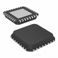
(32 LD QFN)
TOP VIEW
32
31
30
29
28
27
26
25
OFS
3
22
VID4
VCC
4
21
VID3
COMP
5
20
ENLL
FB
6
19
PHASE2
VDIFF
7
18
BOOT2
RGND
8
17
UGATE2
9
10
11
12
13
14
15
16
ISEN2
PHASE1
PVCC
23
LGATE2
2
IREF
REF
ISUM
BOOT1
ICOMP
24
OCSET
1
VSEN
VID12.5
Ordering Information
PART NUMBER
(Notes 2, 3)
PART
MARKING
TEMP. RANGE
(°C)
PACKAGE
(Pb-free)
PKG.
DWG. #
ISL6568CRZ
ISL6568CRZ
0 to +70
32 Ld 5x5 QFN
L32.5x5
ISL6568CRZ-T (Note 1)
ISL6568CRZ
0 to +70
32 Ld 5x5 QFN, Tape and Reel
L32.5x5
ISL6568CRZR5184
ISL6568CRZ
0 to +70
32 Ld 5x5 QFN
L32.5x5
ISL6568CRZ-TR5184 (Note 1)
ISL6568CRZ
0 to +70
32 Ld 5x5 QFN, Tape and Reel
L32.5x5
ISL6568CRZAR5184
ISL6568CRZ
0 to +70
32 Ld 5x5 QFN
L32.5x5
ISL6568CRZA-TR5184 (Note 1)
ISL6568CRZ
0 to +70
32 Ld 5x5 QFN, Tape and Reel
L32.5x5
ISL6568IRZ
ISL6568IRZ
-40 to +85
32 Ld 5x5 QFN
L32.5x5
ISL6568IRZ-T (Note 1)
ISL6568IRZ
-40 to +85
32 Ld 5x5 QFN, Tape and Reel
L32.5x5
ISL6568IRZA
ISL6568IRZ
-40 to +85
32 Ld 5x5 QFN
L32.5x5
ISL6568IRZA-T (Note 1)
ISL6568IRZ
-40 to +85
32 Ld 5x5 QFN, Tape and Reel
L32.5x5
NOTES:
1. Please refer to TB347 for details on reel specifications.
2. These Intersil Pb-free plastic packaged products employ special Pb-free material sets, molding compounds/die attach materials, and 100% matte
tin plate plus anneal (e3 termination finish, which is RoHS compliant and compatible with both SnPb and Pb-free soldering operations). Intersil
Pb-free products are MSL classified at Pb-free peak reflow temperatures that meet or exceed the Pb-free requirements of IPC/JEDEC J STD-020.
3. For Moisture Sensitivity Level (MSL), please see device information page for ISL6568. For more information on MSL please see tech brief TB363.
FN9187 Rev 5.00
Jan 12, 2012
Page 2 of 30
�ISL6568
Block Diagram
ENLL
PGOOD
ICOMP OCSET
100µA
ISEN AMP
0.66V
ISUM
POWER-ON
RESET
OC
IREF
VCC
PVCC
+1V
RGND
VSEN
BOOT1
SOFT START
AND
x1
x1
FAULT LOGIC
UGATE1
SHOOTTHROUGH
PROTECTION
GATE
CONTROL
LOGIC
VDIFF
PHASE1
UVP
LGATE1
0.2V
OVP
CLOCK AND
SAWTOOTH
GENERATOR
FS
OVP
VOVP
PWM1
BOOT2
+150mV
UGATE2
x 0.82
VID4
GATE
CONTROL
LOGIC
PWM2
SHOOTTHROUGH
PROTECTION
PHASE2
VID3
VID2
VID1
LGATE2
DYNAMIC
VID
D/A
VID0
PHASE 2
DETECT
VID12.5
REF
E/A
FB
CHANNEL
CURRENT
BALANCE
COMP
OFS
1
N
OFFSET
CHANNEL
CURRENT
SENSE
ISEN1 ISEN2
FN9187 Rev 5.00
Jan 12, 2012
GND
Page 3 of 30
�ISL6568
Typical Application - ISL6568
VDIFF
FB
COMP
VSEN
RGND
+12V
+5V
PVCC1
VCC
BOOT1
UGATE1
OFS
PHASE1
ISEN1
FS
REF
LGATE1
ISL6568
VID4
VID3
+12V
VID2
PVCC2
VID1
LOAD
VID0
VID12.5
BOOT2
UGATE2
PGOOD
+12V
PHASE2
ISEN2
GND
LGATE2
ENLL
IREF
OCSET
ICOMP
FN9187 Rev 5.00
Jan 12, 2012
ISUM
Page 4 of 30
�ISL6568
Typical Application - ISL6568 with NTC Thermal Compensation
VDIFF
FB
COMP
VSEN
RGND
+12V
+5V
PVCC1
VCC
BOOT1
UGATE1
OFS
PHASE1
ISEN1
FS
REF
LGATE1
VID4
ISL6568
VID3
+12V
VID2
PVCC2
VID1
LOAD
VID0
VID12.5
BOOT2
PLACE IN CLOSE
PROXIMITY
UGATE2
PGOOD
+12V
PHASE2
ISEN2
NTC
GND
LGATE2
ENLL
IREF
OCSET
ICOMP
FN9187 Rev 5.00
Jan 12, 2012
ISUM
Page 5 of 30
�ISL6568
Absolute Maximum Ratings
Thermal Information
Supply Voltage, VCC . . . . . . . . . . . . . . . . . . . . . . . . . . . . . . . . . . . -0.3V to +6V
Supply Voltage, PVCC . . . . . . . . . . . . . . . . . . . . . . . . . . . . . . . . . -0.3V to +15V
Absolute Boot Voltage, VBOOT . . . . . . . . . . . . . . . . GND - 0.3V to GND + 36V
Phase Voltage, VPHASE . . . . . . . . . . . . . . . . GND - 0.3V to 15V (PVCC = 12)
GND - 8V ( -----------------------------2C ESR
2 f 0 V pp L
R C = R FB ----------------------------------------0.66 V IN ESR
0.66V IN ESR C
C C = -----------------------------------------------2V PP R FB f 0 L
FN9187 Rev 5.00
Jan 12, 2012
(EQ. 29)
The optional capacitor C2, is sometimes needed to bypass
noise away from the PWM comparator (See Figure 20). Keep a
position available for C2, and be prepared to install a
high-frequency capacitor of between 22pF and 150pF in case
any leading edge jitter problem is noted.
Output Filter Design
The output inductors and the output capacitor bank together to
form a low-pass filter responsible for smoothing the pulsating
voltage at the phase nodes. The output filter also must provide
the transient energy until the regulator can respond. Because
it has a low bandwidth compared to the switching frequency,
the output filter limits the system transient response. The
output capacitors must supply or sink load current while the
current in the output inductors increases or decreases to meet
the demand.
In high-speed converters, the output capacitor bank is usually
the most costly (and often the largest) part of the circuit. Output
filter design begins with minimizing the cost of this part of the
circuit. The critical load parameters in choosing the output
capacitors are the maximum size of the load step, I, the
load-current slew rate, di/dt, and the maximum allowable
output-voltage deviation under transient loading, VMAX.
Capacitors are characterized according to their capacitance,
ESR, and ESL (equivalent series inductance).
At the beginning of the load transient, the output capacitors
supply all of the transient current. The output voltage will
initially deviate by an amount approximated by the voltage
drop across the ESL. As the load current increases, the voltage
drop across the ESR increases linearly until the load current
reaches its final value. The capacitors selected must have
sufficiently low ESL and ESR so that the total output-voltage
deviation is less than the allowable maximum. Neglecting the
contribution of inductor current and regulator response, the
output voltage initially deviates by an amount as shown by
Equation 30.
di
V ESL ----- + ESR I
dt
(EQ. 30)
The filter capacitor must have sufficiently low ESL and ESR so
that V < VMAX.
Most capacitor solutions rely on a mixture of high frequency
capacitors with relatively low capacitance in combination with
Page 24 of 30
�ISL6568
bulk capacitors having high capacitance but limited
high-frequency performance. Minimizing the ESL of the
high-frequency capacitors allows them to support the output
voltage as the current increases. Minimizing the ESR of the
bulk capacitors allows them to supply the increased current
with less output voltage deviation.
(EQ. 31)
(EQ. 32)
(EQ. 33)
Switching frequency is determined by the selection of the
frequency-setting resistor, RT. Figure 21 and Equation 34 are
provided to assist in selecting the correct value for RT.
FN9187 Rev 5.00
Jan 12, 2012
FIGURE 21. RT vs SWITCHING FREQUENCY
The input capacitors are responsible for sourcing the AC
component of the input current flowing into the upper
MOSFETs. Their RMS current capacity must be sufficient to
handle the ac component of the current drawn by the upper
MOSFETs which is related to duty cycle and the number of
active phases.
0.3
0.2
0.1
IL(P-P) = 0
IL(P-P) = 0.5 IO
IL(P-P) = 0.75 IO
0
0
0.2
0.4
0.6
0.8
1.0
FIGURE 22. NORMALIZED INPUT-CAPACITOR RMS CURRENT FOR
2-PHASE CONVERTER
There are a number of variables to consider when choosing the
switching frequency, as there are considerable effects on the
upper MOSFET loss calculation. These effects are outlined in
“MOSFETs” on page 20, and they establish the upper limit for
the switching frequency. The lower limit is established by the
requirement for fast transient response and small
output-voltage ripple as outlined in “Output Filter Design” on
page 24. Choose the lowest switching frequency that allows
the regulator to meet the transient-response requirements.
10.61 – 1.035 log f S
10000
DUTY CYCLE (VIN/VO)
Switching Frequency
R T = 10
1000
Input Capacitor Selection
Equation 32 gives the upper limit on L for the cases when the
trailing edge of the current transient causes a greater
output-voltage deviation than the leading edge. Equation 33
addresses the leading edge. Normally, the trailing edge
dictates the selection of L because duty cycles are usually less
than 50%. Nevertheless, both inequalities should be
evaluated, and L should be selected based on the lower of the
two results. In each equation, L is the per-channel inductance,
C is the total output capacitance, and N is the number of active
channels.
1.25 N C
L ---------------------------------- V MAX – I ESR V IN – V O
I 2
100
SWITCHINGFREQUENCY (kHz)
Since the capacitors are supplying a decreasing portion of the
load current while the regulator recovers from the transient,
the capacitor voltage becomes slightly depleted. The output
inductors must be capable of assuming the entire load current
before the output voltage decreases more than VMAX. This
places an upper limit on inductance.
2 N C VO
L --------------------------------- V MAX – I ESR
I 2
100
10
10
INPUT-CAPACITOR CURRENT (IRMS/IO)
V – N V
OUT V OUT
IN
L ESR -----------------------------------------------------------f S V IN V P-P MAX
RT (k)
The ESR of the bulk capacitors also creates the majority of the
output-voltage ripple. As the bulk capacitors sink and source
the inductor ac ripple current (See “Interleaving” and
Equation 2 on page 10), a voltage develops across the bulk
capacitor ESR equal to IC(P-P) (ESR). Thus, once the output
capacitors are selected, the maximum allowable ripple
voltage, VP-P(MAX), determines the lower limit on the
inductance as shown by Equation 31.
1000
For a two-phase design, use Figure 22 to determine the
input-capacitor RMS current requirement set by the duty cycle,
maximum sustained output current (IO), and the ratio of the
peak-to-peak inductor current (IL(P-P)) to IO. Select a bulk
capacitor with a ripple current rating which will minimize the
total number of input capacitors required to support the RMS
current calculated. The voltage rating of the capacitors should
also be at least 1.25x greater than the maximum input
voltage. Figure 23 provides the same input RMS current
information for single-phase designs. Use the same approach
for selecting the bulk capacitor type and number.
(EQ. 34)
Page 25 of 30
�ISL6568
When placing the MOSFETs try to keep the source of the upper
FETs and the drain of the lower FETs as close as thermally possible.
Input Bulk capacitors should be placed close to the drain of the
upper FETs and the source of the lower FETs. Locate the output
inductors and output capacitors between the MOSFETs and the load.
The high-frequency input and output decoupling capacitors
(ceramic) should be placed as close as practicable to the decoupling
target, making use of the shortest connection paths to any internal
planes, such as vias to GND next or on the capacitor solder pad.
INPUT-CAPACITOR CURRENT (IRMS/IO)
0.6
0.4
0.2
IL(P-P) = 0
IL(P-P) = 0.5 IO
IL(P-P) = 0.75 IO
0
0
0.2
0.4
0.6
0.8
1.0
DUTY CYCLE (VIN/VO)
FIGURE 23. NORMALIZED INPUT-CAPACITOR RMS CURRENT FOR
SINGLE-PHASE CONVERTER
Low capacitance, high-frequency ceramic capacitors are needed in
addition to the input bulk capacitors to suppress leading and
falling edge voltage spikes. The spikes result from the high current
slew rate produced by the upper MOSFET turn on and off. Select
low ESL ceramic capacitors and place one as close as possible to
each upper MOSFET drain to minimize board parasitics and
maximize suppression.
Layout Considerations
MOSFETs switch very fast and efficiently. The speed with which
the current transitions from one device to another causes voltage
spikes across the interconnecting impedances and parasitic
circuit elements. These voltage spikes can degrade efficiency,
radiate noise into the circuit and lead to device overvoltage
stress. Careful component selection, layout, and placement
minimizes these voltage spikes. Consider, as an example, the
turnoff transition of the upper PWM MOSFET. Prior to turnoff, the
upper MOSFET was carrying channel current. During the turnoff,
current stops flowing in the upper MOSFET and is picked up by
the lower MOSFET. Any inductance in the switched current path
generates a large voltage spike during the switching interval.
Careful component selection, tight layout of the critical
components, and short, wide circuit traces minimize the
magnitude of voltage spikes.
There are two sets of critical components in a DC/DC converter
using a ISL6566 controller. The power components are the most
critical because they switch large amounts of energy. Next, are
small signal components that connect to sensitive nodes or
supply critical bypassing current and signal coupling.
The power components should be placed first, which include the
MOSFETs, input and output capacitors, and the inductors. It is
important to have a symmetrical layout for each power train,
preferably with the controller located equidistant from each.
Symmetrical layout allows heat to be dissipated equally across all
three power trains. Equidistant placement of the controller to the
three power trains also helps keep the gate drive traces equally
short, resulting in equal trace impedances and similar drive
capability of all sets of MOSFETs.
FN9187 Rev 5.00
Jan 12, 2012
The critical small components include the bypass capacitors for
VCC and PVCC, and many of the components surrounding the
controller including the feedback network and current sense
components. Locate the VCC/PVCC bypass capacitors as close to
the ISL6566 as possible. It is especially important to locate the
components associated with the feedback circuit close to their
respective controller pins, since they belong to a high-impedance
circuit loop, sensitive to EMI pick-up. It is also important to place
the current sense components close to their respective pins on
the ISL6566, including RISEN, RS, RCOMP, and CCOMP.
A multi-layer printed circuit board is recommended. Figure 24 shows
the connections of the critical components for the converter. Note
that capacitors CxxIN and CxxOUT could each represent numerous
physical capacitors. Dedicate one solid layer, usually the one
underneath the component side of the board, for a ground plane
and make all critical component ground connections with vias to
this layer. Dedicate another solid layer as a power plane and break
this plane into smaller islands of common voltage levels. Keep the
metal runs from the PHASE terminal to output inductors short. The
power plane should support the input power and output power
nodes. Use copper filled polygons on the top and bottom circuit
layers for the phase nodes. Use the remaining printed circuit layers
for small signal wiring.
Routing UGATE, LGATE, and PHASE Traces
Great attention should be paid to routing the UGATE, LGATE, and
PHASE traces since they drive the power train MOSFETs using
short, high current pulses. It is important to size them as large and
as short as possible to reduce their overall impedance and
inductance. They should be sized to carry at least one ampere of
current (0.02” to 0.05”). Going between layers with vias should also
be avoided, but if so, use two vias for interconnection when possible.
Extra care should be given to the LGATE traces in particular since
keeping their impedance and inductance low helps to significantly
reduce the possibility of shoot-through. It is also important to route
each channels UGATE and PHASE traces in as close proximity as
possible to reduce their inductances.
Thermal Management
For maximum thermal performance in high current, high
switching frequency applications, connecting the thermal GND
pad of the ISL6566 to the ground plane with multiple vias is
recommended. This heat spreading allows the part to achieve
its full thermal potential. It is also recommended that the
controller be placed in a direct path of airflow if possible to help
thermally manage the part.
Page 26 of 30
�ISL6568
Suppressing MOSFET Gate Leakage
With VCC at ground potential, UGATE is high impedance. In this
state, any stray leakage has the potential to deliver charge to the
gate of the upper MOSFET. If UGATE receives sufficient charge to
bias the device on, a low impedance path will be connected
between the upper MOSFET drain and PHASE. If this occurs and
the input power supply is present and active, the system could
see potentially damaging current. Worst-case leakage currents
are on the order of pico-amps; therefore, a 10k resistor,
connected from UGATE to PHASE, is more than sufficient to bleed
off any stray leakage current. This resistor will not affect the
normal performance of the driver or reduce its efficiency.
© Copyright Intersil Americas LLC 2004-2012. All Rights Reserved.
All trademarks and registered trademarks are the property of their respective owners.
For additional products, see www.intersil.com/en/products.html
Intersil products are manufactured, assembled and tested utilizing ISO9001 quality systems as noted
in the quality certifications found at www.intersil.com/en/support/qualandreliability.html
Intersil products are sold by description only. Intersil may modify the circuit design and/or specifications of products at any time without notice, provided that such
modification does not, in Intersil's sole judgment, affect the form, fit or function of the product. Accordingly, the reader is cautioned to verify that datasheets are
current before placing orders. Information furnished by Intersil is believed to be accurate and reliable. However, no responsibility is assumed by Intersil or its
subsidiaries for its use; nor for any infringements of patents or other rights of third parties which may result from its use. No license is granted by implication or
otherwise under any patent or patent rights of Intersil or its subsidiaries.
For information regarding Intersil Corporation and its products, see www.intersil.com
FN9187 Rev 5.00
Jan 12, 2012
Page 27 of 30
�ISL6568
Revision History
The revision history provided is for informational purposes only and is believed to be accurate, but not warranted. Please go to web to make sure you
have the latest revision.
DATE
REVISION
CHANGE
January 3, 2012
FN9187.5
Updated to new Intersil format including Intersil standards.
New part numbers added to “Ordering Information” on page 2 (ISL6568CRZ, ISL6568CRZ-T)
Four obsolete part numbers removed from “Ordering Information” on page 2 (ISL6568IR, ISL6568IR-T,
ISL6568CRR5184, ISL6568CR-TR5184)
Updated POD L32.5x5 to latest revision with the following changes:
Corrected Note 4 from:"Dimension b applies to..." to:
"Dimension applies to.." ("b" leftover from when dimensions were in table format)
Enclosed Note #'s 4, 5 and 6 in a triangle
March 9, 2006
FN9187.4
Changed the Ordering Information on the front page to reflect the new ISL6568 part numbers. Set Customer
Portal attributes for Apple
July 25, 2005
FN9187.3
1) Rewrote the Layout Considerations Section to flow better and provide a better explanation of proper layout
guidelines.
2) Added a "Thermal Management" section to the Layout Considerations section
3) Added a "Suppressing MOSFET Gate Leakage" section to the Layout Considerations section
July 11, 2005
FN9187.2
1) Changed Multiple "Gate Drive Resistance" specs on Page 6
2) All "Gate Drive Resistance" specs are now marked "Parameter magnitude guaranteed by design. Not 100%
tested."
3) Added a spec to page 5 for "Oscillator Frequency" tolerance
4) Added "DAC Input Low and High" specs for AMD mode to page 5
5) Made a change to the Block Diagram on Page 2: added resistors between the LGATE and PHASE pins
6) Made a change to the Application Diagrams on pages 3 and 4: added a capacitors from the IREF pin to ground
7) Made a slight change to the "Pre-POR Overvoltage Protection" section description
October 28, 2004
FN9187.1
Change OFST to OFS throughout
October 22, 2004
FN9187.0
Initial release
Products
Intersil Corporation is a leader in the design and manufacture of high-performance analog semiconductors. The Company's products
address some of the industry's fastest growing markets, such as, flat panel displays, cell phones, handheld products, and notebooks.
Intersil's product families address power management and analog signal processing functions. Go to www.intersil.com/products for a
complete list of Intersil product families.
For a complete listing of Applications, Related Documentation and Related Parts, please see the respective device information page on
intersil.com: ISL6568
To report errors or suggestions for this datasheet, please go to: www.intersil.com/askourstaff
FITs are available from our website at: http://rel.intersil.com/reports/search.php
© Copyright Intersil Americas LLC 2004-2012. All Rights Reserved.
All trademarks and registered trademarks are the property of their respective owners.
For additional products, see www.intersil.com/en/products.html
Intersil products are manufactured, assembled and tested utilizing ISO9001 quality systems as noted
in the quality certifications found at www.intersil.com/en/support/qualandreliability.html
Intersil products are sold by description only. Intersil may modify the circuit design and/or specifications of products at any time without notice, provided that such
modification does not, in Intersil's sole judgment, affect the form, fit or function of the product. Accordingly, the reader is cautioned to verify that datasheets are
current before placing orders. Information furnished by Intersil is believed to be accurate and reliable. However, no responsibility is assumed by Intersil or its
subsidiaries for its use; nor for any infringements of patents or other rights of third parties which may result from its use. No license is granted by implication or
otherwise under any patent or patent rights of Intersil or its subsidiaries.
For information regarding Intersil Corporation and its products, see www.intersil.com
FN9187 Rev 5.00
Jan 12, 2012
Page 28 of 30
�ISL6568
LOCATE CLOSE TO IC
(MINIMIZE CONNECTION PATH)
C2
KEY
HEAVY TRACE ON CIRCUIT PLANE LAYER
RFB
ISLAND ON POWER PLANE LAYER
C1
VDIFF
ISLAND ON CIRCUIT PLANE LAYER
R1
FB
VIA CONNECTION TO GROUND PLANE
COMP
+12V
VSEN
LOCATE NEAR SWITCHING TRANSISTORS;
(MINIMIZE CONNECTION PATH)
RGND
+5V
PVCC
(CF2)
VCC
CBIN1
BOOT1
(CF1)
CBOOT1
UGATE1
ROFS
PHASE1
OFS
ISEN1
RISEN1
FS
RT
LGATE1
REF
CREF
ISL6568
VID4
VID3
CBOUT
+12V
VID2
(CHFOUT)
CBIN2
VID1
LOAD
VID0
BOOT2
VID12.5
CBOOT2
UGATE2
PGOOD
+12V
LOCATE NEAR LOAD;
(MINIMIZE CONNECTION PATH)
PHASE2
ISEN2
GND
RISEN2
LGATE2
ENLL
IREF
OCSET
ICOMP
ISUM
RCOMP
RS
ROCSET
CCOMP
RS
FIGURE 24. PRINTED CIRCUIT BOARD POWER PLANES AND ISLANDS
FN9187 Rev 5.00
Jan 12, 2012
Page 29 of 30
�ISL6568
Package Outline Drawing
L32.5x5
32 LEAD QUAD FLAT NO-LEAD PLASTIC PACKAGE
Rev 3, 4/10
4X 3.5
5.00
28X 0.50
A
B
6
PIN 1
INDEX AREA
6
PIN #1 INDEX AREA
32
25
1
5.00
24
3 .10 ± 0 . 15
17
(4X)
8
0.15
9
16
TOP VIEW
0.10 M C A B
+ 0.07
32X 0.40 ± 0.10
4 32X 0.23 - 0.05
BOTTOM VIEW
SEE DETAIL "X"
0.10 C
0 . 90 ± 0.1
C
BASE PLANE
SEATING PLANE
0.08 C
( 4. 80 TYP )
(
( 28X 0 . 5 )
SIDE VIEW
3. 10 )
(32X 0 . 23 )
C
0 . 2 REF
5
( 32X 0 . 60)
0 . 00 MIN.
0 . 05 MAX.
DETAIL "X"
TYPICAL RECOMMENDED LAND PATTERN
NOTES:
1. Dimensions are in millimeters.
Dimensions in ( ) for Reference Only.
2. Dimensioning and tolerancing conform to AMSE Y14.5m-1994.
3. Unless otherwise specified, tolerance : Decimal ± 0.05
4. Dimension applies to the metallized terminal and is measured
between 0.15mm and 0.30mm from the terminal tip.
5. Tiebar shown (if present) is a non-functional feature.
6. The configuration of the pin #1 identifier is optional, but must be
located within the zone indicated. The pin #1 indentifier may be
either a mold or mark feature.
FN9187 Rev 5.00
Jan 12, 2012
Page 30 of 30
�


 工商网监
湘ICP备2023018690号
工商网监
湘ICP备2023018690号
