PD- 95223
IRLL3303PbF
Surface Mount l Dynamic dv/dt Rating l Logic-Level Gate Drive l Fast Switching l Ease of Paralleling l Advanced Process Technology l Ultra Low On-Resistance l Lead-Free Description
l
HEXFET® Power MOSFET
D
VDSS = 30V
G S
RDS(on) = 0.031Ω ID = 4.6A
Fifth Generation HEXFETs from International Rectifier utilize advanced processing techniques to achieve extremely low on-resistance per silicon area. This benefit, combined with the fast switching speed and ruggedized device design that HEXFET Power MOSFETs are well known for, provides the designer with an extremely efficient and reliable device for use in a wide variety of applications. The SOT-223 package is designed for surface-mount using vapor phase, infra red, or wave soldering techniques. Its unique package design allows for easy automatic pickand-place as with other SOT or SOIC packages but has the added advantage of improved thermal performance due to an enlarged tab for heatsinking. Power dissipation of 1.0W is possible in a typical surface mount application.
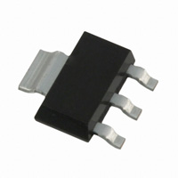
S O T -22 3
Absolute Maximum Ratings
Parameter
ID @ TA = 25°C ID @ TA = 25°C ID @ TA = 70°C IDM PD @TA = 25°C PD @TA = 25°C VGS EAS IAR EAR dv/dt TJ, TSTG Continuous Drain Current, VGS @ 10V** Continuous Drain Current, VGS @ 10V* Continuous Drain Current, VGS @ 10V* Pulsed Drain Current Power Dissipation (PCB Mount)** Power Dissipation (PCB Mount)* Linear Derating Factor (PCB Mount)* Gate-to-Source Voltage Single Pulse Avalanche Energy Avalanche Current Repetitive Avalanche Energy Peak Diode Recovery dv/dt Junction and Storage Temperature Range
Max.
6.5 4.6 3.7 37 2.1 1.0 8.3 ± 16 140 4.6 0.10 1.3 -55 to + 150
Units
A
W W
mW/°C
V mJ A mJ V/ns °C
Thermal Resistance
Parameter
RθJA RθJA Junction-to-Amb. (PCB Mount, steady state)* Junction-to-Amb. (PCB Mount, steady state)**
Typ.
93 48
Max.
120 60
Units
°C/W
* When mounted on FR-4 board using minimum recommended footprint. ** When mounted on 1 inch square copper board, for comparison with other SMD devices.
www.irf.com
1
04/27/04
�IRLL3303PbF
Electrical Characteristics @ TJ = 25°C (unless otherwise specified)
V(BR)DSS
∆V(BR)DSS/∆TJ
Parameter Drain-to-Source Breakdown Voltage Breakdown Voltage Temp. Coefficient Static Drain-to-Source On-Resistance Gate Threshold Voltage Forward Transconductance Drain-to-Source Leakage Current Gate-to-Source Forward Leakage Gate-to-Source Reverse Leakage Total Gate Charge Gate-to-Source Charge Gate-to-Drain ("Miller") Charge Turn-On Delay Time Rise Time Turn-Off Delay Time Fall Time Input Capacitance Output Capacitance Reverse Transfer Capacitance
RDS(on) VGS(th) gfs IDSS IGSS Qg Qgs Qgd td(on) tr td(off) tf Ciss Coss Crss
Min. 30 ––– ––– ––– 1.0 5.5 ––– ––– ––– ––– ––– ––– ––– ––– ––– ––– ––– ––– ––– –––
Typ. ––– 0.034 ––– ––– ––– ––– ––– ––– ––– ––– 34 4.4 10 7.2 22 33 28 840 340 170
Max. Units Conditions ––– V VGS = 0V, ID = 250µA ––– V/°C Reference to 25°C, ID = 1mA 0.031 VGS = 10V, ID = 4.6A Ω 0.045 VGS = 4.5V, ID = 2.3A ––– V VDS = VGS, ID = 250µA ––– S VDS = 10V, ID = 2.3A 25 VDS = 30V, VGS = 0V µA 250 VDS = 24V, VGS = 0V, TJ = 125°C -100 VGS = -16V nA 100 VGS = 16V 50 ID = 4.6A 6.5 nC VDS = 24V 16 VGS = 10V, See Fig. 6 and 9 ––– VDD = 15V ––– ID = 4.6A ns ––– R G = 6.2Ω ––– R D = 3.2Ω, See Fig. 10 ––– VGS = 0V ––– pF VDS = 25V ––– ƒ = 1.0MHz, See Fig. 5
Source-Drain Ratings and Characteristics
IS
ISM
VSD trr Qrr ton
Parameter Continuous Source Current (Body Diode) Pulsed Source Current (Body Diode) Diode Forward Voltage Reverse Recovery Time Reverse RecoveryCharge Forward Turn-On Time
Min. Typ. Max. Units
Conditions MOSFET symbol ––– ––– 0.91 showing the A integral reverse ––– ––– 37 p-n junction diode. ––– ––– 1.3 V TJ = 25°C, IS = 4.6A, VGS = 0V ––– 65 98 ns TJ = 25°C, IF = 4.6A ––– 160 240 nC di/dt = 100A/µs Intrinsic turn-on time is negligible (turn-on is dominated by LS+LD)
Specification changes
Rev. #
1 1 Notes:
Parameters
VGS(th) (Max.) VGS (Max.)
Old spec.
2.5V ±20
New spec.
No spec. ±16
Comments
Removed V GS(th) (Max). Specification Decrease VGS (Max). Specification
Revision Date
11/1/96 11/1/96
Repetitive rating; pulse width limited by
max. junction temperature. ( See fig. 11 )
ISD ≤ 4.6A, di/dt ≤ 110A/µs, VDD ≤ V(BR)DSS,
TJ ≤ 150°C
VDD = 15V, starting TJ = 25°C, L = 13mH
RG = 25Ω, IAS = 4.6A. (See Figure 12)
Pulse width ≤ 300µs; duty cycle ≤ 2%.
2
www.irf.com
�IRLL3303PbF
100
V GS 15V 10V 7.0V 5.5V 4.5V 4.0V 3.5V BOT TOM 3.0V TO P
100
I D , D rain-to-Source C urrent (A)
10
I D, D rain-to-Source C urrent (A )
VGS 15V 10V 7.0V 5.5V 4.5V 4.0V 3.5V BOTTOM 3.0V TOP
10
3 .0V
3 .0V
1 0.1 1
2 0 µ s P U LS E W ID TH TJ = 2 5°C A
10
1 0.1 1
2 0 µ s P U L S E W ID TH TJ = 15 0°C A
10
V D S , D rain-to-S ourc e V olta g e ( V )
V D S, D rain-to-S ource V olta g e (V )
Fig 1. Typical Output Characteristics
Fig 2. Typical Output Characteristics
100
2.0
R D S (on) , Drain-to-S ource O n Resistance (N orm alized)
I D = 4 .6A
I D , D rain-to-So urce C urren t (A )
1.5
TJ = 2 5 °C TJ = 1 5 0 ° C
10
1.0
0.5
1 3.0 3.5 4.0
V DS= 10V 2 0 µ s P U L S E W ID T H
4.5 5.0 5.5
A
0.0 -60 -40 -20 0 20 40 60 80
V G S = 10 V
100 120
140 160
A
V G S , G a te -to -S o u rc e V o lta g e (V )
T J , Junction T em perature (°C )
Fig 3. Typical Transfer Characteristics
Fig 4. Normalized On-Resistance Vs. Temperature
www.irf.com
3
�IRLL3303PbF
1600 1400 20
V G S , G ate-to-Source V oltage (V )
C i ss C , Capacitance (pF)
1200 1000 800 600 400 200 0 1
V GS C iss C rs s C o ss
= = = =
0V , f = 1MHz C g s + C g d , C d s S H O R TE D C gd C ds + C g d
I D = 4.6 A V D S = 2 4V V D S = 1 5V
16
C o ss
12
8
C r ss
4
A
10 100
0 0 10 20
F O R TE S T C IR C U IT S E E F IG U R E 9
30 40 50
A
V D S , D rain-to-S ourc e V olta g e ( V )
Q G , T otal G ate C har g e ( nC )
Fig 5. Typical Capacitance Vs. Drain-to-Source Voltage
Fig 6. Typical Gate Charge Vs. Gate-to-Source Voltage
100
100
I S D , R everse Drain C urrent (A )
O P E R A TIO N IN TH IS A R E A L IM ITE D B Y R D S (o n)
I D , Drain C urrent (A )
100µs 10
10
TJ = 1 5 0°C
T J = 2 5°C
1m s
1 0.4 0.6 0.8 1.0
V G S = 0V
1.2
A
1
T A = 2 5 °C T J = 15 0°C S in g le P u lse
0.1 1 10
10m s
1.4
A
100
V S D , S ourc e-to-D rain V olta g e ( V )
V D S , D rain-to-S ource V olta g e ( V )
Fig 7. Typical Source-Drain Diode Forward Voltage
Fig 8. Maximum Safe Operating Area
4
www.irf.com
�IRLL3303PbF
QG
VDS VGS
RD
10V
VG
QGS
QGD
D.U.T.
+
RG
- VDD
10V
Charge
Pulse Width ≤ 1 µs Duty Factor ≤ 0.1 %
Fig 9a. Basic Gate Charge Waveform
Current Regulator Same Type as D.U.T.
Fig 10a. Switching Time Test Circuit
VDS
50KΩ 12V .2µF .3µF
90%
D.U.T. VGS
3mA
+ V - DS
10% VGS
td(on)
IG ID
tr
t d(off)
tf
Current Sampling Resistors
Fig 9b. Gate Charge Test Circuit
1000
Fig 10b. Switching Time Waveforms
T herm al R es pons e (Z th J A )
100 D = 0 .5 0 0 .2 0 10 0 .1 0 0 .0 5 0 .02 1 0 .01
PD M
t
0.1 S IN G L E P U L S E (TH E R M A L R E S P O N S E )
1 t2
N o te s : 1 . D u ty fac t or D = t
1
/t
2
0.01 0.00001
2 . P e a k TJ = P D M x Z th J A + T A
A
10000
0.0001
0.001
0.01
0.1
1
10
100
1000
t 1 , R e cta n g u la r P u lse D u ra tio n (se c )
Fig 11. Maximum Effective Transient Thermal Impedance, Junction-to-Ambient
www.irf.com
5
�IRLL3303PbF
350
E A S , S ingle P ulse A valanche E nergy (m J)
TO P
300
1 5V
B O TTO M
250
ID 2.1 A 3.7A 4 .6 A
VD S
L
D R IV E R
200
RG
20V
D .U .T
IA S tp 0 .01 Ω
+ - VD D
150
A
100
Fig 12a. Unclamped Inductive Test Circuit
50
0
V DD = 15 V
25 50 75 100 125
A
150
V (B R )D SS tp
S tartin g T J , J unc tion T em p erature ( °C )
Fig 12c. Maximum Avalanche Energy Vs. Drain Current
IAS
Fig 12b. Unclamped Inductive Waveforms
6
www.irf.com
�IRLL3303PbF
Peak Diode Recovery dv/dt Test Circuit
D.U.T
+
+
Circuit Layout Considerations • Low Stray Inductance • Ground Plane • Low Leakage Inductance Current Transformer
-
+
RG • • • • dv/dt controlled by RG Driver same type as D.U.T. ISD controlled by Duty Factor "D" D.U.T. - Device Under Test
+ VDD
Driver Gate Drive P.W. Period D=
P.W. Period VGS=10V
*
D.U.T. ISD Waveform Reverse Recovery Current Body Diode Forward Current di/dt D.U.T. VDS Waveform Diode Recovery dv/dt
VDD
Re-Applied Voltage Inductor Curent
Body Diode
Forward Drop
Ripple ≤ 5%
ISD
* VGS = 5V for Logic Level Devices Fig 13. For N-Channel HEXFETS
www.irf.com
7
�IRLL3303PbF
SOT-223 (TO-261AA) Package Outline
Dimensions are shown in milimeters (inches)
SOT-223 (TO-261AA) Part Marking Information
HEXFET PRODUCT MARKING
T HIS IS AN IRF L014
INT ERNATIONAL RECTIF IER LOGO
PART NUMBER
LOT CODE AXXXX
FL014 314P
A = ASS EMBLY SITE DAT E CODE CODE (YYWW) YY = YEAR WW = WEEK P = DES IGNATES LEAD-F REE PRODUCT (OPT IONAL)
TOP
BOTT OM
8
www.irf.com
�IRLL3303PbF
SOT-223 (TO-261AA) Tape & Reel Information
Dimensions are shown in milimeters (inches)
4 .1 0 ( .1 6 1 ) 3 .9 0 ( .1 5 4 ) 0 .3 5 ( .0 1 3 ) 0 .2 5 ( .0 1 0 )
TR
2 .0 5 ( .0 8 0 ) 1 .9 5 ( .0 7 7 )
1 .8 5 ( .0 7 2 ) 1 .6 5 ( .0 6 5 )
7 .5 5 ( .2 9 7 ) 7 .4 5 ( .2 9 4 ) 7 .6 0 ( .2 9 9 ) 7 .4 0 ( .2 9 2 ) 1 .6 0 ( .0 6 2 ) 1 .5 0 ( .0 5 9 ) TYP . F E E D D IR E C T IO N 1 2 .1 0 ( .4 7 5 ) 1 1 .9 0 ( .4 6 9 ) NOTES : 1 . C O N T R O L L IN G D IM E N S IO N : M IL L IM E T E R . 2 . O U T L IN E C O N F O R M S T O E IA -4 8 1 & E IA -5 4 1 . 3 . E A C H O 3 30 .0 0 ( 1 3 .0 0 ) R E E L C O N T A IN S 2 ,5 0 0 D E V IC E S . 1 3 .2 0 ( .5 1 9 ) 1 2 .8 0 ( .5 0 4 ) 1 5 .40 ( .6 0 7 ) 1 1 .90 ( .4 6 9 ) 4 7 .1 0 ( .2 7 9 ) 6 .9 0 ( .2 7 2 )
1 6 .3 0 ( .6 4 1 ) 1 5 .7 0 ( .6 1 9 )
2 .3 0 ( .0 9 0 ) 2 .1 0 ( .0 8 3 )
330.00 ( 13.000 ) M AX.
5 0.00 ( 1 .9 6 9 ) M IN .
NO TE S : 1 . O U T LIN E C O M F O R M S T O E IA -4 1 8 -1 . 2 . C O N T R O L L IN G D IM E N S IO N : M IL L IM E T E R .. 3 . D IM E N S IO N M E A S U R E D @ H U B . 4 . IN C L U D E S F L A N G E D IS T O R T IO N @ O U T E R E D G E .
1 4 .4 0 ( .5 6 6 ) 1 2 .4 0 ( .4 8 8 ) 3
1 8 .4 0 ( .72 4 ) M AX . 4
Data and specifications subject to change without notice.
IR WORLD HEADQUARTERS: 233 Kansas St., El Segundo, California 90245, USA Tel: (310) 252-7105 TAC Fax: (310) 252-7903 Visit us at www.irf.com for sales contact information. 04/04
www.irf.com
9
�


 工商网监
湘ICP备2023018690号
工商网监
湘ICP备2023018690号
