ISOCOM
COMPONENTS
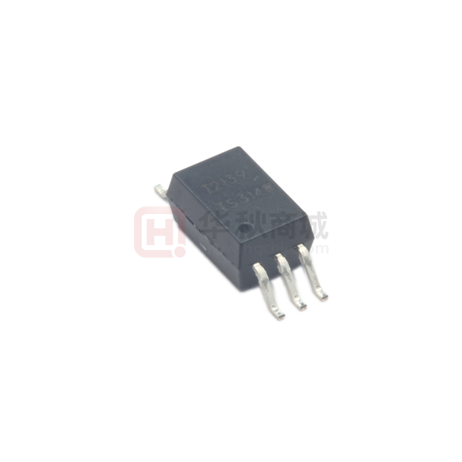
IS314W
DESCRIPTION
1 Anode
The IS314W Photocoupler is ideally suited for driving
power IGBTs and MOSFETs used in inverters of
motor control and of power supply system. It contains
an AlGaAs LED optically coupled to an integrated
circuit with a power output stage.
2 NC
3 Cathode
4 GND (VEE)
The device is in Stretched SO6 package.
5 VO
6 VCC
FEATURES
•
•
•
•
•
•
•
•
•
•
•
•
•
1.0A Maximum Peak Output Current
0.8A Minimum Peak Output Current
Rail-to-Rail output voltage
20kV/μs Minimum Common Mode Rejection
at VCM 1500V
Maximum Propagation Delay 200ns
Maximum Propagation Delay Difference 100ns
Wide Operating Voltage Range
VCC 10 to 30 V
Maximum Supply Current ICC 3.0mA
Under Voltage Lock Out (UVLO) Protection with
Hysteresis
Guaranteed Performance over
Temperature Range - 40°C to +105°C
MSL Level 1
Lead Free and RoHS Compliant
Safety Approvals Pending
A 0.1μF bypass Capacitor must be connected between Pins 6 and 4.
ABSOLUTE MAXIMUM RATINGS (TA = 25°C)
Stresses exceeding the absolute maximum ratings can cause
permanent damage to the device.
Exposure to absolute maximum ratings for long periods of time
can adversely affect reliability.
Input
Forward Current
Forward Peak Current
(Pulse Width ≤ 1μs, 300pps)
Reverse Voltage
Forward Current Rise / Fall Time
Power dissipation
•
•
•
•
•
IGBT/MOSFET Gate Drive
UPS
Inverters
Switching Power Supplies
AC Brushless and DC Motor Drives
ORDER INFORMATION
•
Supplied in Tape & Reel
ISOCOM COMPONENTS 2004 LTD
Unit 25B, Park View Road West, Park View Industrial Estate
Hartlepool, Cleveland, TS25 1PE, United Kingdom
Tel: +44 (0)1429 863 609 Fax : +44 (0)1429 863 581
e-mail: sales@isocom.co.uk
http://www.isocom.com
1 13/10/2016
5V
500ns
45mW
Output
High Level Peak Output Current
APPLICATIONS
25mA
1.0A
1.0A
Exponential waveform.
Pulse width ≤ 0.3 µs, f ≤ 15 kHz
Low Level Peak Output Current
1.0A
Exponential waveform.
Pulse width ≤ 0.3 µs, f ≤ 15 kHz
Supply Voltage (VCC ̶ VEE)
35V
Output Voltage
VCC
Power Dissipation
250mW
Total Package
Isolation Voltage
Total Power Dissipation
Operating Temperature
Storage Temperature
Lead Soldering Temperature (10s)
5000VRMS
295mW
-40 to 105 °C
-55 to 125 °C
260°C
ISOCOM COMPONENTS ASIA LTD
Hong Kong Office,
Block A, 8/F, Wah Hing Industrial mansion,
36 Tai Yau Street, San Po Kong, Kowloon, Hong Kong.
Tel: +852 2995 9217 Fax : +852 8161 6292
e-mail sales@isocom.com.hk
DC93194
�ISOCOM
COMPONENTS
IS314W
Truth Table
LED
High Side
Low Side
VO
OFF
OFF
ON
LOW
ON
ON
OFF
HIGH
Recommended Operating Conditions
Parameter
Symbol
Min
Max
Unit
TA
- 40
105
°C
VCC ̶ VEE
10
30
V
Input Current (ON)
IF(ON)
7
16
mA
Input Voltage (OFF)
VF(OFF)
-3.0
0.8
V
Operating Temperature
Supply Voltage
2 13/10/2016
DC93194
�ISOCOM
COMPONENTS
IS314W
ELECTRICAL CHARACTERISTICS (Typical Values at VCC
̶ VEE = 10V to 30V and TA = 25°C,
Minimum and Maximum Values at Recommended Operating Conditions,
unless otherwise specified)
INPUT
Parameter
Symbol
Test Condition
Min
Typ.
Max
Unit
Forward Voltage
VF
IF = 10mA
1.2
1.37
1.8
V
Forward Voltage
Temperature
Coefficient
ΔVF/ΔT
IF = 10mA
Reverse Voltage
VR
IR = 10μA
Input Threshold Current
(Low to High)
IFLH
VO > 5V, IO = 0A
Input Threshold Voltage
(High to Low)
VFHL
VO < 5V, IO = 0A
Input Capacitance
CIN
VF = 0V, f = 1MHz
Symbol
Test Condition
High Level
Supply Current
ICCH
Low Level
Supply Current
High Level
Output Current
OUTPUT
Parameter
Low Level
Output Current
̶ 1.237
mV/°C
5
V
1.9
5
mA
0.8
V
33
Typ.
Max
Unit
IF = 7 to 16mA
VO = Open
1.9
3.0
mA
ICCL
VF = ̶ 3 to 0.8V
VO = Open
2.1
3.0
mA
IOH
VO = VCC – 1.5V
Pulse Width = 50μs
̶ 0.3
A
VO = VCC – 3V
Pulse Width = 10μs
̶ 0.8
IOL
Min
pF
VO = VEE + 1.5V
Pulse Width = 50μs
0.3
VO = VEE + 3V
Pulse Width = 10μs
0.8
VCC ̶ 0.6
A
High Level
Output Voltage
VOH
IF = 10mA, IO = -100mA
Low Level
Output Voltage
VOL
IF = 0mA, IO = 100mA
VUVLO+
VO > 5V, IF = 10mA
7.8
V
VUVLO-
VO < 5V, IF = 10mA
6.7
V
1.1
V
UVLO Threshold
UVLO Hysteresis
3 13/10/2016
UVLOHYS
VCC ̶ 0.35
V
VEE +0.25 VEE +0.4
V
DC93194
�ISOCOM
COMPONENTS
IS314W
ELECTRICAL CHARACTERISTICS (Typical Values at VCC
̶ VEE = 10V to 30V and TA = 25°C,
Minimum and Maximum Values at Recommended Operating Conditions,
unless otherwise specified)
SWITCHING
Parameter
Symbol
Test Condition
Min
Typ.
Max
Unit
Propagation Delay Time
to High Output Level
tPLH
50
120
200
ns
Propagation Delay Time
to Low Output Level
tPHL
50
110
200
Pulse Width Distortion
|tPHL - tPLH| for any given
device
PWD
IF = 7 to 16mA,
VCC = 15 to 30V,
VEE = 0V
Rg = 47Ω,
Cg = 3nF,
f = 10kHz,
Duty Cycle = 50%
20
70
Propagation Delay
Difference (tPHL - tPLH)
between any two
Devices
PDD
-100
100
Output Rise Time
(10% to 90%)
tr
35
Output Fall Time
(90% to 10%)
tf
35
Common Mode
Transient Immunity at
High Output Level
CMH
IF = 10 to 16mA,
VCC = 30V
VCM = 1500V,
TA = 25°C
20
25
kV/μs
Common Mode
Transient Immunity at
Low Output Level
CML
VF = 0V,
VCC = 30V
VCM = 1500V,
TA = 25°C
20
25
kV/μs
4 13/10/2016
DC93194
�ISOCOM
COMPONENTS
IS314W
ELECTRICAL CHARACTERISTICS (Typical Values at VCC
̶ VEE = 10V to 30V and TA = 25°C,
Minimum and Maximum Values at Recommended Operating Conditions,
unless otherwise specified)
ISOLATION
Parameter
Symbol
Test Condition
Min
Typ.
Max
Unit
Insulation Voltage
VISO
RH ≤ 40% to 60%,
t = 1 min, TA = 25°C
5000
Input - Output
Resistance
RI-O
VI-O = 500VDC
1012
Ω
Input - Output
Capacitance
CI-O
f = 1MHz, TA = 25°C
0.92
pF
V
Note :
1.
A 0.1uF or bigger bypass capacitor must be connected across pin 6 and pin 4.
2.
PDD is the difference of tPHL and tPLH between any two IS314W devices under same test conditions.
3.
CMH, Common Mode Transient Immunity in High stage is the maximum tolerable positive dVCM/dt on the leading edge of the common
mode impulse signal, VCM, to assure that the output will remain high (VO > 15V).
4.
CML, Common Mode Transient Immunity in Low stage is the maximum tolerable negative dVCM/dt on the trailing edge of the common
mode impulse signal, VCM, to assure that the output will remain low (VO < 1V).
5 13/10/2016
DC93194
�ISOCOM
COMPONENTS
IS314W
Fig 1 Forward Current vs Forward Voltage
Fig 2 Supply Current vs Supply Voltage
Fig 3 Supply Current vs Ambient Temperature
Fig 4 Low Level Output Voltage vs
Ambient temperature
Fig 5 High Level Output Voltage vs
Ambient Temperature
Fig 6 High Output Voltage Drop vs
Ambient Temperature
6 13/10/2016
DC93194
�ISOCOM
COMPONENTS
IS314W
Fig 7 IFLH Hysteresis
Fig 8 Input Threshold Current vs
Ambient Temperature
Fig 9 Propagation Delay vs Supply Voltage
Fig 10 Propagation Delay vs Forward Current
Fig 11 Propagation Delay vs Series Load Resistance
Fig 12 Propagation Delay vs Series Load Capacitance
7 13/10/2016
DC93194
�ISOCOM
COMPONENTS
IS314W
Fig 13 Propagation Delay vs Ambient Temperature
VOH Test Circuit
VOL Test Circuit
8 13/10/2016
DC93194
�ISOCOM
COMPONENTS
IS314W
IOH Test Circuit
IOL Test Circuit
IFLH Test Circuit
9 13/10/2016
DC93194
�ISOCOM
COMPONENTS
IS314W
UVLO Test Circuit
tr, tf, tPLH and tPHL Test Circuit and Waveform
10 13/10/2016
DC93194
�ISOCOM
COMPONENTS
IS314W
CMR Test Circuit and Waveform
11 13/10/2016
DC93194
�ISOCOM
COMPONENTS
IS314W
ORDER INFORMATION
IS314W
After PN
None
PN
Description
Packing quantity
IS314W
Stretched SO6
1000 pcs per reel
DEVICE MARKING
IYYWW
IS314W
IS314W
denotes Device Part Number
I
denotes Isocom
YY
denotes 2 digit Year code
WW
denotes 2 digit Week code
12 13/10/2016
DC93194
�ISOCOM
COMPONENTS
IS314W
PACKAGE DIMENSIONS and Recommended PCB Pad Layout in mm (inch)
13 13/10/2016
DC93194
�ISOCOM
COMPONENTS
IS314W
TAPE AND REEL PACKAGING
Description
Symbol
Dimension
mm (inch)
Tape Width
W
16 ± 0.3 (0.63)
Pitch of Sprocket Holes
P0
4 ± 0.1 (0.16)
F
7.5 ± 0.1 (0.3)
P2
2 ± 0.1 (0.079)
P1
16 ± 0.1 (0.63)
Distance of Compartment to Sprocket Holes
Distance of Compartment to Compartment
14 13/10/2016
DC93194
�ISOCOM
COMPONENTS
IS314W
IR REFLOW SOLDERING TEMPERATURE PROFILE
(One Time Reflow Soldering is Recommended)
TP
260°C
TP - 5°C
Max Ramp Up Rate
3°C/s
TEMP (°C)
TL
Tsmax
Tsmin
tP
Max Ramp Down Rate
6°C/s
217°C
TL
200°C
150°C
ts Preheat
60s – 120s
25°C
TIME (s)
Time 25°C to Peak Temperature
Profile Details
Conditions
Preheat
- Min Temperature (TSMIN)
- Max Temperature (TSMAX)
- Time TSMIN to TSMAX (ts)
150°C
200°C
60s - 120s
Soldering Zone
- Peak Temperature (TP)
- Time at Peak Temperature
- Liquidous Temperature (TL)
- Time within 5°C of Actual Peak Temperature (TP ̶ 5°C)
- Time maintained above TL (tL)
- Ramp Up Rate (TL to TP)
- Ramp Down Rate (TP to TL)
260°C
10s max
217°C
30s max
60s - 100s
3°C/s max
6°C/s max
Average Ramp Up Rate (Tsmax to TP)
3°C/s max
Time 25°C to Peak Temperature
8 minutes max
15 13/10/2016
DC93194
�ISOCOM
COMPONENTS
IS314W
NOTES :
- Isocom is continually improving the quality, reliability, function or design and Isocom reserves the right to make
changes without further notices.
- The products shown in this publication are designed for the general use in electronic applications such as
office automation equipment, communications devices, audio/visual equipment, electrical application and
instrumentation.
- For equipment/application where high reliability or safety is required, such as space applications, nuclear power
control equipment, medical equipment, etc., please contact our sales representatives.
- When requiring a device for any ”specific” application, please contact our sales for advice.
- The contents described herein are subject to change without prior notice.
- Do not immerse device body in solder paste.
16 13/10/2016
DC93194
�ISOCOM
COMPONENTS
DISCLAIMER
ISOCOM is continually working to improve the quality and reliability of its products.
Nevertheless, semiconductor devices in general can malfunction or fail due to their inherent
electrical sensitivity and vulnerability to physical stress. It is the responsibility of the buyer,
when utilizing ISOCOM products, to comply with the standards of safety in making a safe
design for the entire system, and to avoid situations in which a malfunction or failure of such
ISOCOM products could cause loss of human life, bodily injury or damage to property.
In developing your designs, please ensure that ISOCOM products are used within specified
operating ranges as set forth in the most recent ISOCOM products specifications.
__ The ISOCOM products listed in this document are intended for usage in general
electronics applications (computer, personal equipment, office equipment, measuring
equipment, industrial robotics, domestic appliances, etc.). These ISOCOM products are
neither intended nor warranted for usage in equipment that requires extraordinarily high quality
and/or reliability or a malfunction or failure of which may cause loss of human life or bodily
injury (“Unintended Usage”). Unintended Usage include atomic energy control instruments,
airplane or spaceship instruments, transportation Instruments, traffic signal instruments,
combustion control instruments, medical Instruments, all types of safety devices, etc..
Unintended Usage of ISOCOM products listed in this document shall be made at the
customer’s own risk.
__ Gallium arsenide (GaAs) is a substance used in the products described in this document.
GaAs dust and fumes are toxic. Do not break, cut or pulverize the product, or use chemicals to
dissolve them. When disposing of the products, follow the appropriate regulations. Do not
dispose of the products with other industrial waste or with domestic garbage.
__ The products described in this document are subject to the foreign exchange and foreign
trade laws.
__ The information contained herein is presented only as a guide for the applications of our
products. No responsibility is assumed by ISOCOM Components for any infringements of
intellectual property or other rights of the third parties which may result from its use. No license
is granted by implication or otherwise under any intellectual property or other rights of
ISOCOM Components or others.
__ The information contained herein is subject to change without notice.
17 13/10/2016
Dxxxxxx
�


 工商网监
湘ICP备2023018690号
工商网监
湘ICP备2023018690号
