IS43TR16640AL-125JBLI 数据手册
IS43/46TR16640A/AL, IS43/46TR81280A/AL
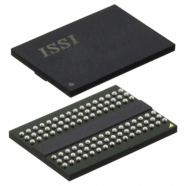
128Mx8, 64Mx16 1Gb DDR3 SDRAM
ADVANCED INFORMATION
DECEMBER 2011
FEATURES
Standard Voltage: VDD and VDDQ = 1.5V ± 0.075V
Low Voltage (L): VDD and VDDQ = 1.35V + 0.1V, -0.067V
Refresh Interval:
7.8 us (8192 cycles/64 ms) Tc= -40°C to 85°C
3.9 us (8192 cycles/32 ms) Tc= 85°C to 105°C
High speed data transfer rates with system
frequency up to 933 MHz
8 internal banks for concurrent operation
8Bits pre-fetch architecture
Programmable CAS Latency: 5, 6, 7, 8, 9, 10 and
11
Programmable Additive Latency: 0, CL-1,CL-2
Programmable CAS WRITE latency (CWL) based
on tCK
Programmable Burst Length: 4 and 8
Programmable Burst Sequence: Sequential or
Interleave
BL switch on the fly
Auto Self Refresh(ASR)
Self Refresh Temperature(SRT)
OPTIONS
Configuration:
128Mx8
64Mx16
Package:
96-ball FBGA (9mm x 13mm) for x16
78-ball FBGA (8mm x 10.5mm) for x8
Partial Array Self Refresh
Asynchronous RESET pin
TDQS (Termination Data Strobe) supported (x8
only)
OCD (Off-Chip Driver Impedance Adjustment)
Dynamic ODT (On-Die Termination)
Driver strength : RZQ/7, RZQ/6 (RZQ = 240 Ω)
Write Leveling
Operating temperature:
Commercial (TC = 0°C to +95°C)
Industrial (TC = -40°C to +95°C)
Automotive, A1 (TC = -40°C to +95°C)
Automotive, A2 (TC = -40°C to +105°C)
ADDRESS TABLE
Parameter
Row Addressing
Column Addressing
Bank Addressing
Page size
Auto Precharge Addressing
BL switch on the fly
128Mx8
A0-A13
A0-A9
BA0-2
1KB
A10/AP
A12/BC#
64Mx16
A0-A12
A0-A9
BA0-2
2KB
A10/AP
A12/BC#
SPEED BIN
Speed Option
JEDEC Speed Grade
CL-nRCD-nRP
tRCD,tRP(min)
187F
15G
15H
125J
125K
107K
107L
DDR31066F
7-7-7
13.125
DDR31333G
8-8-8
12.0
DDR31333H
9-9-9
13.5
DDR31600J
10-10-10
12.5
DDR31600K
11-11-11
13.75
DDR31866K
11-11-11
11.77
DDR31866L
12-12-12
12.84
Units
tCK
ns
Note: Faster speed options are backward compatible to slower speed options.
Copyright © 2011 Integrated Silicon Solution, Inc. All rights reserved. ISSI reserves the right to make changes to this specification and its products at any time
without notice. ISSI assumes no liability arising out of the application or use of any information, products or services described herein. Customers are advised
to obtain the latest version of this device specification before relying on any published information and before placing orders for products.
Integrated Silicon Solution, Inc. does not recommend the use of any of its products in life support applications where the failure or malfunction of the product
can reasonably be expected to cause failure of the life support system or to significantly affect its safety or effectiveness. Products are not authorized for use
in such applications unless Integrated Silicon Solution, Inc. receives written assurance to its satisfaction, that:
a.) the risk of injury or damage has been minimized;
b.) the user assume all such risks; and
c.) potential liability of Integrated Silicon Solution, Inc is adequately protected under the circumstances
Integrated Silicon Solution, Inc. – www.issi.com –
Rev. 00A
12/12/2011
1
�IS43/46TR16640A/AL, IS43/46TR81280A/AL
1. DDR3 PACKAGE BALLOUT
1.1 DDR3 SDRAM package ballout 78-ball FBGA – x8
1
VSS
2
VDD
B
VSS
VSSQ
C
D
VDDQ
DQ2
VSSQ
DQ6
E
VREFDQ
F
NC1
G
H
J
K
VDD
L
VSS
M
VDD
N
VSS
A
3
NC
4
5
6
7
NU/TDQS#
8
VSS
9
VDD
DQ0
DM/TDQS
VSSQ
VDDQ
DQS
DQ1
DQ3
VSSQ
DQS#
VDD
VSS
VSSQ
VDDQ
DQ4
DQ7
DQ5
VDDQ
VSS
RAS#
CK
VSS
NC
ODT
VDD
CAS#
CK#
VDD
CKE
NC
CS#
WE#
A10/AP
ZQ
NC
VSS
BA0
BA2
A15
VREFCA
VSS
A3
A0
A12/BC#
BA1
VDD
A5
A2
A1
A4
VSS
A7
A9
A11
A6
VDD
RESET#
A13
NC/A14
A8
VSS
Note:
NC balls have no internal connection. NC/14 and NC/15 are one of NC pins and reserved for higher densities.
1.2 DDR3 SDRAM package ballout 96-ball FBGA – x16
A
1
VDDQ
2
DQU5
3
DQU7
VDD
4
5
6
7
DQU4
8
VDDQ
9
VSS
VSS
DQSU#
DQU6
VSSQ
VDDQ
B
VSSQ
C
D
VDDQ
DQU3
DQU1
DQSU
DQU2
VSSQ
VDDQ
DMU
DQU0
VSSQ
VDD
E
VSS
VSSQ
DQL0
DML
VSSQ
VDDQ
F
VDDQ
DQL2
DQSL
DQL1
DQL3
VSSQ
G
VSSQ
DQL6
DQSL#
VDD
VSS
VSSQ
H
VREFDQ
VDDQ
DQL4
DQL7
DQL5
VDDQ
J
K
NC
VSS
RAS#
CK
VSS
NC
ODT
VDD
CAS#
CK#
VDD
CKE
L
NC
CS#
WE#
A10/AP
ZQ
NC
M
VSS
BA0
BA2
NC/A15
VREFCA
VSS
N
A12/BC#
BA1
VDD
VDD
A3
A0
P
VSS
A5
A2
A1
A4
VSS
R
T
VDD
A7
A9
A11
A6
VDD
VSS
RESET#
NC/A13
NC/A14
A8
VSS
Note:
NC balls have no internal connection. NC/13, NC/14 and NC/15 are one of NC pins and reserved for higher densities.
Integrated Silicon Solution, Inc. – www.issi.com –
Rev. 00A
12/12/2011
2
�IS43/46TR16640A/AL, IS43/46TR81280A/AL
1.3 Pinout Description - JEDEC Standard
Symbol
Type
Function
CK, CK#
Input
CKE, (CKE0),
(CKE1)
Input
CS#, (CS0#),
(CS1#), (CS2#),
(CS3#)
ODT, (ODT0),
(ODT1)
Input
Clock: CK and CK# are differential clock inputs. All address and control input signals are sampled
on the crossing of the positive edge of CK and negative edge of CK#.
Clock Enable: CKE HIGH activates, and CKE Low deactivates, internal clock signals and device
input buffers and output drivers. Taking CKE Low provides Precharge Power-Down and SelfRefresh operation (all banks idle), or Active Power-Down (row Active in any bank). CKE is
asynchronous for Self-Refresh exit. After VREFCA and VREFDQ have become stable during the
power on and initialization sequence, they must be maintained during all operations (including
Self-Refresh). CKE must be maintained high throughout read and write accesses. Input buffers,
excluding CK, CK#, ODT and CKE, are disabled during power-down. Input buffers, excluding
CKE, are disabled during Self-Refresh.
Chip Select: All commands are masked when CS# is registered HIGH. CS# provides for external
Rank selection on systems with multiple Ranks. CS# is considered part of the command code.
RAS#. CAS#.
WE#
DM, (DMU),
(DML)
Input
BA0 - BA2
Input
A0 - A13
Input
A10 / AP
Input
A12 / BC#
Input
RESET#
Input
DQ
Input / Output
DQU, DQL, DQS,
DQS#, DQSU,
DQSU#, DQSL,
DQSL#
Input / Output
TDQS, TDQS#
Output
Input
Input
NC
On Die Termination: ODT (registered HIGH) enables termination resistance internal to the DDR3
SDRAM. When enabled, ODT is only applied to each DQ, DQSU, DQSU#, DQSL, DQSL#, DMU,
and DML signal. The ODT pin will be ignored if MR1 and MR2 are programmed to disable RTT.
Command Inputs: RAS#, CAS# and WE# (along with CS#) define the command being entered.
Input Data Mask: DM is an input mask signal for write data. Input data is masked when DM is
sampled HIGH coincident with that input data during a Write access. DM is sampled on both
edges of DQS. For x8 device, the function of DM or TDQS/TDQS# is enabled by Mode Register
A11 setting in MR1.
Bank Address Inputs: BA0 - BA2 define to which bank an Active, Read, Write, or Precharge
command is being applied. Bank address also determines which mode register is to be accessed
during a MRS cycle.
Address Inputs: Provide the row address for Active commands and the column address for Read/
Write commands to select one location out of the memory array in the respective bank. (A10/AP
and A12/BC# have additional functions; see below). The address inputs also provide the op-code
during Mode Register Set commands.
Auto-precharge: A10 is sampled during Read/Write commands to determine whether
Autoprecharge should be performed to the accessed bank after the Read/Write operation. (HIGH:
Autoprecharge; LOW: no Autoprecharge). A10 is sampled during a Precharge command to
determine whether the Precharge applies to one bank (A10 LOW) or all banks (A10 HIGH). If
only one bank is to be precharged, the bank is selected by bank addresses.
Burst Chop: A12 / BC# is sampled during Read and Write commands to determine if burst chop
(on-the-fly) will be performed. (HIGH, no burst chop; LOW: burst chopped). See command truth
table for details.
Active Low Asynchronous Reset: Reset is active when RESET# is LOW, and inactive when
RESET# is HIGH. RESET# must be HIGH during normal operation. RESET# is a CMOS rail- torail signal with DC high and low at 80% and 20% of VDD, i.e., 1.20V for DC high and 0.30V for
DC low.
Data Input/ Output: Bi-directional data bus.
Data Strobe: output with read data, input with write data. Edge-aligned with read data, centered
in write data. For the x16, DQSL corresponds to the data on DQL0-DQL7; DQSU corresponds to
the data on DQU0-DQU7. The data strobes DQS, DQSL, and DQSU are paired with differential
signals DQS#, DQSL#, and DQSU#, respectively, to provide differential pair signaling to the
system during reads and writes. DDR3 SDRAM supports differential data strobe only and does
not support single-ended.
Termination Data Strobe: TDQS/TDQS# is applicable for x8 DRAMs only. When enabled via
Mode Register A11 = 1 in MR1, the DRAM will enable the same termination resistance function
on TDQS/TDQS# that is applied to DQS/DQS#. When disabled via mode register A11 = 0 in
MR1, DM/TDQS will provide the data mask function and TDQS# is not used. x16 DRAMs must
disable the TDQS function via mode register A11 = 0 in MR1.
No Connect: No internal electrical connection is present.
VDDQ
Supply
DQ Power Supply: 1.5 V +/- 0.075 V for standard voltage or 1.35V +0.1V, -0.067V for low voltage
VSSQ
Supply
DQ Ground
Integrated Silicon Solution, Inc. – www.issi.com –
Rev. 00A
12/12/2011
3
�IS43/46TR16640A/AL, IS43/46TR81280A/AL
VDD
Supply
Power Supply: 1.5 V +/- 0.075 V for standard voltage or 1.35V +0.1V, -0.067V for low voltage
VSS
Supply
Ground
VREFDQ
Supply
Reference voltage for DQ
VREFCA
Supply
Reference voltage for CA
ZQ, (ZQ0), (ZQ1),
(ZQ2), (ZQ3)
Supply
Reference Pin for ZQ calibration Input only pins (BA0-BA2, A0-A13, RAS#, CAS#, WE#, CS#,
CKE, ODT, and RESET#) do not supply termination.
Integrated Silicon Solution, Inc. – www.issi.com –
Rev. 00A
12/12/2011
4
�IS43/46TR16640A/AL, IS43/46TR81280A/AL
ORDERING INFORMATION
64Mx16 - Commercial Range: (0°C ≤ TC ≤ 95°C)
Data Rate
CL-tRCD-tRP
Order Part No.
Package
1066MT/s
1333MT/s
7-7-7
8-8-8
IS43TR16640A -187FBL
IS43TR16640A -15GBL
96-ball FBGA,Lead-free
96-ball FBGA,Lead-free
1333MT/s
1600MT/s
1600MT/s
9-9-9
10-10-10
11-11-11
IS43TR16640A -15HBL
IS43TR16640A -125JBL
IS43TR16640A -125KBL
96-ball FBGA,Lead-free
96-ball FBGA,Lead-free
96-ball FBGA,Lead-free
64Mx16 - Industrial Range: (–40°C ≤ TC ≤ 95°C)
Data Rate
CL-tRCD-tRP
Order Part No.
Package
1066MT/s
1333MT/s
1333MT/s
7-7-7
8-8-8
9-9-9
IS43TR16640A -187FBLI
IS43TR16640A -15GBLI
IS43TR16640A -15HBLI
96-ball FBGA,Lead-free
96-ball FBGA,Lead-free
96-ball FBGA,Lead-free
1600MT/s
1600MT/s
10-10-10
11-11-11
IS43TR16640A -125JBLI
IS43TR16640A -125KBLI
96-ball FBGA,Lead-free
96-ball FBGA,Lead-free
64Mx16 – Automotive, A1 Range: (–40°C ≤ TC ≤ 95°C)
Data Rate
CL-tRCD-tRP
Order Part No.
Package
1066MT/s
1333MT/s
1333MT/s
1600MT/s
1600MT/s
7-7-7
8-8-8
9-9-9
10-10-10
11-11-11
IS46TR16640A -187FBLA1
IS46TR16640A -15GBLA1
IS46TR16640A -15HBLA1
IS46TR16640A -125JBLA1
IS46TR16640A -125KBLA1
96-ball FBGA,Lead-free
96-ball FBGA,Lead-free
96-ball FBGA,Lead-free
96-ball FBGA,Lead-free
96-ball FBGA,Lead-free
64Mx16 – Automotive, A2 Range: (–40°C ≤ TC ≤ 105°C)
Data Rate
CL-tRCD-tRP
Order Part No.
Package
1066MT/s
1333MT/s
1333MT/s
1600MT/s
1600MT/s
7-7-7
8-8-8
9-9-9
10-10-10
11-11-11
IS46TR16640A -187FBLA2
IS46TR16640A -15GBLA2
IS46TR16640A -15HBLA2
IS46TR16640A -125JBLA2
IS46TR16640A -125KBLA2
96-ball FBGA,Lead-free
96-ball FBGA,Lead-free
96-ball FBGA,Lead-free
96-ball FBGA,Lead-free
96-ball FBGA,Lead-free
Note: Contact ISSI for availability of options.
Integrated Silicon Solution, Inc. – www.issi.com –
Rev. 00A
12/12/2011
5
�IS43/46TR16640A/AL, IS43/46TR81280A/AL
ORDERING INFORMATION
128Mx8 - Commercial Range: (0°C ≤ TC ≤ 95°C)
Data Rate
CL-tRCD-tRP
Order Part No.
Package
1066MT/s
7-7-7
IS43TR81280A -187FBL
78-ball FBGA,Lead-free
1333MT/s
8-8-8
IS43TR81280A -15GBL
78-ball FBGA,Lead-free
1333MT/s
9-9-9
IS43TR81280A -15HBL
78-ball FBGA,Lead-free
1600MT/s
10-10-10
IS43TR81280A -125JBL
78-ball FBGA,Lead-free
1600MT/s
11-11-11
IS43TR81280A -125KBL
78-ball FBGA,Lead-free
128Mx8 - Industrial Range: (–40°C ≤ TC ≤ 95°C)
Data Rate
CL-tRCD-tRP
Order Part No.
Package
1066MT/s
7-7-7
IS43TR81280A -187FBLI
78-ball FBGA,Lead-free
1333MT/s
8-8-8
IS43TR81280A -15GBLI
78-ball FBGA,Lead-free
1333MT/s
9-9-9
IS43TR81280A -15HBLI
78-ball FBGA,Lead-free
1600MT/s
10-10-10
IS43TR81280A -125JBLI
78-ball FBGA,Lead-free
1600MT/s
11-11-11
IS43TR81280A -125KBLI
78-ball FBGA,Lead-free
128Mx8 – Automotive, A1 Range: (–40°C ≤ TC ≤ 95°C)
Data Rate
CL-tRCD-tRP
Order Part No.
Package
1066MT/s
7-7-7
IS46TR81280A -187FBLA1
78-ball FBGA,Lead-free
1333MT/s
8-8-8
IS46TR81280A -15GBLA1
78-ball FBGA,Lead-free
1333MT/s
9-9-9
IS46TR81280A -15HBLA1
78-ball FBGA,Lead-free
1600MT/s
10-10-10
IS46TR81280A -125JBLA1
78-ball FBGA,Lead-free
1600MT/s
11-11-11
IS46TR81280A -125KBLA1
78-ball FBGA,Lead-free
128Mx8 – Automotive, A2 Range: (–40°C ≤ TC ≤ 105°C)
Data Rate
CL-tRCD-tRP
Order Part No.
Package
1066MT/s
7-7-7
IS46TR81280A -187FBLA2
78-ball FBGA,Lead-free
1333MT/s
8-8-8
IS46TR81280A -15GBLA2
78-ball FBGA,Lead-free
1333MT/s
9-9-9
IS46TR81280A -15HBLA2
78-ball FBGA,Lead-free
1600MT/s
10-10-10
IS46TR81280A -125JBLA2
78-ball FBGA,Lead-free
1600MT/s
11-11-11
IS46TR81280A -125KBLA2
78-ball FBGA,Lead-free
Note: Contact ISSI for availability of options.
Integrated Silicon Solution, Inc. – www.issi.com –
Rev. 00A
12/12/2011
6
�IS43/46TR16640A/AL, IS43/46TR81280A/AL
PACKAGE OUTLINE DRAWING
78-ball BGA (8mm x 10.5mm): 0.8mm x 0.8mm Pitch (x8)
Bottom View
6.40
Max. 1.20
Min. 0.25
Max. 0.40
9.60
10.50 +/- 0.10
0.8
0.8
Min 0.1
Min 0.1
8.00 +/- 0.10
Integrated Silicon Solution, Inc. – www.issi.com –
Rev. 00A
12/12/2011
78 x ø Min. 0.40
Max. 0.50
7
�IS43/46TR16640A/AL, IS43/46TR81280A/AL
PACKAGE OUTLINE DRAWING
96-ball BGA (9mm x 13mm): 0.8mm x 0.8mm Pitch (x16)
Max. 1.20
Bottom View
Min. 0.25
Max. 0.40
6.40
12.00
13.00 +/- 0.10
0.8
0.8
Min 0.1
Min 0.1
9.00 +/- 0.10
Integrated Silicon Solution, Inc. – www.issi.com –
Rev. 00A
12/12/2011
96 x ø Min. 0.40
Max. 0.50
8
�


 工商网监
湘ICP备2023018690号
工商网监
湘ICP备2023018690号
