VDSS
ID (cont)
RDS(on)
trr
IXFH 6N120
High Voltage
HiPerFET Power
MOSFET
= 1200 V
=
6 A
= 2.6 Ω
≤ 300 ns
N-Channel Enhancement Mode
Avalanche Rated
Preliminary Data Sheet
Symbol
Test Conditions
Maximum Ratings
VDSS
VDGR
TJ = 25°C to 150°C
TJ = 25°C to 150°C; RGS = 1 MΩ
VGS
VGSM
Continuous
Transient
ID25
TC = 25°C
IDM
TC = 25°C, pulse width limited by TJM
IAR
1200
1200
V
V
±20
±30
V
V
6
A
24
A
TC = 25°C
6
A
EAR
TC = 25°C
25
mJ
EAS
TC = 25°C
500
mJ
dv/dt
IS ≤ IDM, di/dt ≤ 100 A/µs, VDD ≤ VDSS,
10
V/ns
300
W
-55 ... +150
150
-55 ... +150
°C
°C
°C
z
300
°C
z
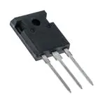
TO-247 AD (IXTH)
(TAB)
G = Gate,
S = Source,
D = Drain,
TAB = Drain
TJ ≤ 150°C, RG = 2 Ω
PD
TC = 25°C
TJ
TJM
Tstg
TL
1.6 mm (0.062 in.) from case for 10 s
Md
Mounting torque
Weight
TO-247 AD
1.13/10 Nm/lb.in.
6
Features
z
z
z
g
International standard packages
Low RDS (on) HDMOSTM process
Rugged polysilicon gate cell structure
Unclamped Inductive Switching (UIS)
rated
Low package inductance
- easy to drive and to protect
Advantages
z
z
Symbol
Test Conditions
(TJ = 25°C, unless otherwise specified)
Characteristic Values
Min. Typ.
Max.
VDSS
VGS = 0 V, ID = 250 µA
VGS(th)
VDS = VGS, ID =2.5 mA
IGSS
VGS = ±20 VDC, VDS = 0
IDSS
VDS = VDSS
VGS = 0 V
RDS(on)
VGS = 10 V, ID = 0.5 ID25
Pulse test, t ≤ 300 µs, duty cycle d ≤ 2 %
© 2005 IXYS All rights reserved
1200
3.0
TJ = 25°C
TJ = 125°C
z
Easy to mount
Space savings
High power density
V
5.0
V
±100
nA
50
1500
µA
µA
2.6
Ω
DS99335(02/05)
�IXFH 6N120
Symbol
Test Conditions
Characteristic Values
(TJ = 25°C, unless otherwise specified)
Min. Typ. Max.
gfs
VDS = 20 V; ID = 0.5 ID25, pulse test
5
S
1950
pF
175
pF
C rss
60
pF
td(on)
28
ns
Ciss
Coss
VGS = 0 V, VDS = 25 V, f = 1 MHz
3
tr
V GS = 10 V, VDS = 0.5 VDSS, ID = 0.5 ID25
33
ns
td(off)
RG = 4.7 Ω (External)
42
ns
tf
18
ns
Qg(on)
56
nC
13
nC
25
nC
Qgs
VGS = 10 V, VDS = 0.5 VDSS, ID = 0.5 ID25
Qgd
RthJC
RthCK
0.42
(TO-247)
Source-Drain Diode
0.21
K/W
K/W
Characteristic Values
(TJ = 25°C, unless otherwise specified)
min. typ. max.
Symbol
Test Conditions
IS
VGS = 0 V
6
A
ISM
Repetitive
24
A
VSD
IF = IS, VGS = 0 V,
Pulse test, t ≤ 300 µs, duty cycle d ≤ 2 %
IF = 6 A, di/dt ≤ 100 A/µs
1.5
V
trr
QRM
IRM
300
0.6
3.0
TO-247 AD Outline
1
2
3
Terminals: 1 - Gate
3 - Source
Dim.
2 - Drain
Tab - Drain
Millimeter
Min.
Max.
A
4.7
5.3
A1
2.2
2.54
A2
2.2
2.6
b
1.0
1.4
b1
1.65
2.13
b2
2.87
3.12
C
.4
.8
D
20.80 21.46
E
15.75 16.26
e
5.20
5.72
L
19.81 20.32
L1
4.50
∅P 3.55
3.65
Q
5.89
6.40
R
4.32
5.49
S
6.15 BSC
Inches
Min. Max.
.185 .209
.087 .102
.059 .098
.040 .055
.065 .084
.113 .123
.016 .031
.819 .845
.610 .640
0.205 0.225
.780 .800
.177
.140 .144
0.232 0.252
.170 .216
242 BSC
ns
uC
A
IXYS reserves the right to change limits, test conditions, and dimensions.
IXYS MOSFETs and IGBTs are covered by one or more
of the following U.S. patents:
4,835,592 4,881,106 5,017,508 5,049,961 5,187,117 5,486,715 6,306,728B1 6,259,123B1 6,306,728B1
4,850,072 4,931,844 5,034,796 5,063,307 5,237,481 5,381,025 6,404,065B1 6,162,665
6,534,343
�IXFH 6N120
Fig. 2. Extended Output Characteristics
@ 25 deg. C
Fig. 1. Output Characteristics
@ 25 Deg. C
10
6
VGS = 10V
9V
8V
7V
4
VGS = 10V
9V
8V
7V
8
ID - Amperes
ID - Amperes
5
6V
3
2
6
2
5V
1
6V
4
5V
0
0
0
2
4
6
8
10
12
14
16
0
5
10
V DS - Volts
Fig. 3. Output Characteristics
25
30
Junction Temperature
6
3.1
VGS = 10V
9V
8V
7V
6V
4
VGS = 10V
2.8
RDS(on) - Normalized
5
ID - Amperes
20
Fig. 4. RDS(on) Normalized to ID25 Value vs.
@ 125 Deg. C
3
2
5V
1
2.5
2.2
1.9
ID = 6A
1.6
1.3
ID = 3A
1
0.7
0.4
0
0
5
10
15
20
25
-50
30
-25
V DS - Volts
0
25
50
75
100
125
150
TJ - Degrees Centigrade
Fig. 6. Drain Current vs. Case
Temperature
Fig. 5. RDS(on) Normalized to I D25
Value vs. I D
7
2.8
VGS = 10V
2.5
6
T J = 125ºC
5
2.2
ID - Amperes
RDS(on) - Normalized
15
V DS - Volts
1.9
1.6
T J = 25ºC
1.3
4
3
2
1
1
0
0.7
0
1.5
3
4.5
6
ID - Amperes
© 2005 IXYS All rights reserved
7.5
9
-50
-25
0
25
50
75
100
TC - Degrees Centigrade
125
150
�IXFH 6N120
Fig. 8. Transconductance
6
12
5
10
4
8
Gfs - Siemens
ID - Amperes
Fig. 7. Input Admittance
T J = -40ºC
25ºC
125ºC
3
2
1
T J = -40ºC
25ºC
125ºC
6
4
2
0
0
3.5
4
4.5
5
5.5
6
6.5
0
1.5
3
V GS - Volts
Fig. 9. Source Current vs. Source-To-Drain
Voltage
6
7.5
9
Fig. 10. Gate Charge
20
10
16
8
VGS - Volts
IS - Amperes
4.5
ID - Amperes
12
8
T J = 125ºC
4
VDS = 600V
ID = 3A
IG = 10mA
6
4
2
T J = 25ºC
0
0
0.4
0.5
0.6
0.7
0.8
0.9
0
V SD - Volts
10
20
30
40
50
60
QG - nanoCoulombs
Fig. 12. Maximum Transient Thermal
Resistance
Fig. 11. Capacitance
10000
1
C iss
1000
R(th)JC - (ºC/W)
Capacitance - pF
f = 1M hz
C oss
100
0.1
C rss
10
0.01
0
5
10
15
20
25
30
35
40
V DS - Volts
1
10
100
1000
Pulse Width - milliseconds
IXYS reserves the right to change limits, test conditions, and dimensions.
IXYS MOSFETs and IGBTs are covered by one or more
of the following U.S. patents:
4,835,592 4,881,106 5,017,508 5,049,961 5,187,117 5,486,715 6,306,728B1 6,259,123B1 6,306,728B1
4,850,072 4,931,844 5,034,796 5,063,307 5,237,481 5,381,025 6,404,065B1 6,162,665
6,534,343
�Disclaimer Notice - Information furnished is believed to be accurate and reliable. However, users should independently
evaluate the suitability of and test each product selected for their own applications. Littelfuse products are not designed for,
and may not be used in, all applications. Read complete Disclaimer Notice at www.littelfuse.com/disclaimer-electronics.
�


 工商网监
湘ICP备2023018690号
工商网监
湘ICP备2023018690号
