HiPerFETTM
Power MOSFET
VDSS
Symbol Test Conditions
Maximum Ratings
TJ = 25∞C to 150∞C
TJ = 25∞C to 150∞C, RGS = 1MΩ
VGS
VGSM
Continuous
Transient
ID25
TC = 25°C
24N100
23N100
24N100
23N100
1000
1000
V
V
±20
±30
V
V
A
A
A
A
A
IDM
T C = 25°C;
IAR
TC = 25°C
24
23
96
92
24
EAR
EAS
TC = 25°C
TC = 25°C
60
3
mJ
J
dv/dt
IS ≤ IDM, di/dt ≤ 100 A/µs, VDD ≤ VDSS
TJ ≤ 150°C, RG = 2 Ω
5
V/ns
PD
TC = 25°C
600
W
-55 ... +150
150
-55 ... +150
°C
°C
°C
300
°C
2500
3000
V~
V~
Note 1
TJ
TJM
Tstg
TL
1.6 mm (0.063 in) from case for 10 s
VISOL
50/60 Hz, RMS
IISOL ≤ 1 mA
Md
Mounting torque
Terminal connection torque
t = 1 min
t=1s
1.5/13 Nm/lb.in.
1.5/13 Nm/lb.in.
Weight
30
g
Symbol
Test Conditions
(TJ = 25°C, unless otherwise specified)
Min.
Characteristic Values
Typ.
Max.
VDSS
VGS = 0 V, ID = 3mA
1000
V
VGS(th)
VDS = VGS, ID = 8mA
3.0
IGSS
VGS = ±20V, VGS = 0V
IDSS
VDS = VDSS
VGS = 0 V
TJ = 25°C
TJ = 125°C
100 µA
2 mA
RDS(on)
VGS = 10V, ID = 0.5 ï ID25
Note 2
23N100
24N100
0.43
0.39
© 2005 IXYS All rights reserved
RDS(on)
0.39 Ω
0.43 Ω
IXFN 24N100 1000 V 24 A
IXFN 23N100 1000 V 23 A
trr ≤ 250 ns
Single MOSFET Die
VDSS
VDGR
ID25
5.5
V
±100 nA
Ω
Ω
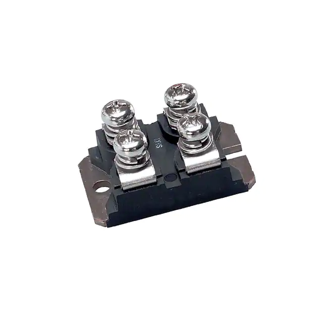
miniBLOC, SOT-227 B (IXFN)
E153432
S
G
S
D
G = Gate
S = Source
D = Drain
Either Source terminal at miniBLOC can be used
as Main or Kelvin Source
Features
• International standard package
• Encapsulating epoxy meets
UL 94 V-0, flammability classification
• miniBLOC with Aluminium nitride
isolation
• Low RDS (on) HDMOSTM process
• Rugged polysilicon gate cell structure
• Unclamped Inductive Switching (UIS)
rated
• Low package inductance
• Fast intrinsic Rectifier
Applications
• DC-DC converters
• Synchronous rectification
• Battery chargers
• Switched-mode and resonant-mode
power supplies
• DC choppers
• Temperature and lighting controls
• Low voltage relays
Advantages
• Easy to mount
• Space savings
• High power density
98597E (07/05)
�IXFN 23N100
IXFN 24N100
Symbol
Test Conditions
(TJ = 25°C, unless otherwise specified)
gfs
Characteristic Values
Min. Typ. Max.
VDS = 10 V; ID = 0.5 ï ID25, Note 2
15
miniBLOC, SOT-227 B
22
S
7000
pF
750
pF
Crss
260
pF
td(on)
35
ns
35
ns
75
ns
21
ns
Dim.
250
nC
A
B
31.50
7.80
55
nC
C
D
135
nC
Ciss
Coss
VGS = 0 V, VDS = 25 V, f = 1 MHz
tr
VGS = 10 V, VDS = 0.5 ï VDSS, ID = 0.5 ï ID25
td(off)
RG
= 1 Ω (External),
tf
Qg(on)
Qgs
VGS = 10 V, VDS = 0.5 ï VDSS, ID = 0.5 ï ID25
Qgd
RthJC
0.21
RthCK
0.05
Source-Drain Diode
(TJ = 25°C, unless otherwise specified)
Symbol
Test Conditions
Max.
1.240
0.307
1.255
0.323
4.09
4.09
4.29
4.29
0.161
0.161
0.169
0.169
E
F
4.09
14.91
4.29
15.11
0.161
0.587
0.169
0.595
K/W
G
H
30.12
38.00
30.30
38.23
1.186
1.496
1.193
1.505
K/W
J
K
11.68
8.92
12.22
9.60
0.460
0.351
0.481
0.378
L
M
0.76
12.60
0.84
12.85
0.030
0.496
0.033
0.506
N
O
25.15
1.98
25.42
2.13
0.990
0.078
1.001
0.084
P
Q
4.95
26.54
5.97
26.90
0.195
1.045
0.235
1.059
R
S
3.94
4.72
4.42
4.85
0.155
0.186
0.174
0.191
T
U
24.59
-0.05
25.07
0.1
0.968
-0.002
0.987
0.004
VGS = 0
24N100
23N100
24
23
A
A
ISM
Repetitive;
pulse width limited by TJM
24N100
23N100
96
92
A
A
VSD
IF = IS, VGS = 0 V,
Pulse test, t ≤ 300 µs, duty cycle d ≤ 2 %
1.5
V
250
ns
µC
A
1.0
8
Notes: 1. Pulse width limited by TJM.
2. Pulse test, t ≤ 300 ms, duty cycle d ≤ 2 %.
IXYS reserves the right to change limits, test conditions, and dimensions.
IXYS MOSFETs and IGBTs are covered by
one or moreof the following U.S. patents:
4,835,592
4,850,072
4,881,106
4,931,844
5,017,508
5,034,796
5,049,961
5,063,307
5,187,117
5,237,481
5,381,025
5,486,715
6,162,665
6,259,123 B1
6,306,728 B1
Inches
31.88
8.20
Characteristic Values
Min. Typ. Max.
I F = IS, -di/dt = 100 A/µs, V R = 100 V
Millimeter
Min.
Max.
Min.
IS
t rr
QRM
IRM
M4 screws (4x) supplied
6,404,065 B1
6,534,343
6,583,505
6,683,344
6,710,405B2
6,710,463
6,727,585
6,759,692
6771478 B2
�IXFN 23N100
IXFN 24N100
50
20
TJ = 25∞C
VGS = 8-10V
TJ = 25∞C
7V
40
VGS = 10V
9V
8V
7V
6V
10
ID - Amperes
ID - Amperes
15
5
30
20
6V
10
5V
5V
0
0
0
2
4
6
8
0
10
5
Figure 1. Output Characteristics at 25OC
20
25
Figure 2. Extended Output Characteristics at 125OC
20
TJ = 125∞C VGS = 10V
9V
8V
7V
6V
15
ID - Amperes
16
ID - Amperes
15
VCE - Volts
VDS - Volts
20
10
12
8
O
TJ = 125 C
10
TJ = 25OC
5
4
5V
0
0
0
4
8
12
16
20
VDS - Volts
2.4
RDS(ON) - Normalized
VGS = 10V
2.0
1.8
ID = 24A
1.6
1.4
ID = 12A
1.2
1.0
0.8
25
50
75
100
125
150
TJ - Degrees C
Figure 5. RDS(on) normalized to 0.5 ID25 value vs. TJ
© 2005 IXYS All rights reserved
4
5
6
VGS - Volts
Figure 3. RDS(on) normalized to 0.5 ID25 value vs. ID
2.2
3
Figure 4. Admittance Curves
7
8
�IXFN 23N100
IXFN 24N100
20000
15
VDS = 500 V
ID = 12 A
IG = 10 mA
Capacitance - pF
VGS - Volts
12
Ciss
10000
9
6
f = 1MHz
Coss
1000
3
Crss
100
0
0
50
100
150
200
250
300
0
350
5
10
50
30
40
25
ID - Amperes
ID - Amperes
25
30
35
40
100
125
150
Figure 7. Capacitance Curves
Figure 6. Gate Charge
TJ = 125oC
20
20
VDS - Volts
Gate Charge - nC
30
15
TJ = 25oC
10
20
15
10
5
0
0.0
0.5
1.0
1.5
2.0
2.5
0
-50
VSD - Volts
-25
0
25
50
75
Case Temperature - oC
Figure 8. Forward Voltage Drop of the Intrinsic Diode
Figure9. Drain Current vs. Case Temperature
0.300
R(th)JC - K/W
0.100
0.010
0.001
10-4
10-3
10-2
Figure 10. Transient Thermal Resistance
IXYS reserves the right to change limits, test conditions, and dimensions.
10-1
100
101
�


 工商网监
湘ICP备2023018690号
工商网监
湘ICP备2023018690号
