Advance Technical Information
IXTA230N04T4
IXTP230N04T4
TrenchT4TM
Power MOSFET
VDSS
ID25
RDS(on)
N-Channel Enhancement Mode
Avalanche Rated
= 40V
= 230A
2.9m
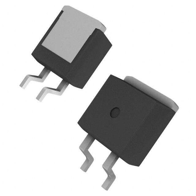
TO-263 AA (IXTA)
G
S
Symbol
Test Conditions
Maximum Ratings
VDSS
TJ = 25C to 175C
40
V
VDGR
TJ = 25C to 175C, RGS = 1M
40
V
VGSM
Transient
15
V
ID25
ILRMS
TC = 25C
Lead Current Limit, RMS
230
160
A
A
IDM
TC = 25C, Pulse Width Limited by TJM
700
A
IA
EAS
TC = 25C
TC = 25C
100
600
A
mJ
PD
TC = 25C
340
W
-55 ... +175
175
-55 ... +175
C
C
C
300
260
°C
°C
1.13 / 10
Nm/lb.in.
2.5
3.0
g
g
TJ
TJM
Tstg
TL
TSOLD
Maximum Lead Temperature for Soldering
1.6 mm (0.062in.) from Case for 10s
Md
Mounting Torque
Weight
TO-263
TO-220
(TO-220)
D (Tab)
TO-220AB (IXTP)
G
DS
G = Gate
S = Source
D (Tab)
D
= Drain
Tab = Drain
Features
International Standard Packages
175°C Operating Temperature
High Current Handling Capability
Avalanche Rated
Low RDS(on)
Advantages
Symbol
Test Conditions
(TJ = 25C Unless Otherwise Specified)
Characteristic Values
Min. Typ.
Max.
BVDSS
VGS = 0V, ID = 250A
40
VGS(th)
VDS = VGS, ID = 250A
2.0
IGSS
VGS = 15V, VDS = 0V
IDSS
VDS = VDSS, VGS = 0V
V
Applications
V
• Synchronous Buck Converters
• High Current Switching Power
200 nA
5
TJ = 150C
RDS(on)
4.0
VGS = 10V, ID = 0.5 • ID25, Notes 1,2
© 2016 IXYS CORPORATION, All Rights Reserved
Easy to Mount
Space Savings
High Power Density
A
250 A
2.9 m
Supplies
• Battery Powered Electric Motors
• Resonant-Mode Power Supplies
• Electronics Ballast Application
• Class D Audio Amplifiers
DS100729(5/16)
�IXTA230N04T4
IXTP230N04T4
Symbol
Test Conditions
(TJ = 25C, Unless Otherwise Specified)
gfs
VDS = 10V, ID = 60A, Note 1
RGi
Gate Input Resistance
Characteristic Values
Min. Typ.
Max.
100
Ciss
Coss
VGS = 0V, VDS = 25V, f = 1MHz
170
S
1.2
7400
pF
1115
pF
760
pF
40
ns
143
ns
Crss
td(on)
tr
td(off)
tf
Resistive Switching Times
VGS = 10V, VDS = 0.5 • VDSS, ID = 0.5 • ID25
RG = 10 (External)
Qg(on)
Qgs
VGS = 10V, VDS = 0.5 • VDSS, ID = 0.5 • ID25
Qgd
RthJC
RthCS
TO-263 (IXTA) Outline
TO-220
85
ns
82
ns
140
nC
35
nC
53
nC
0.50
0.44 C/W
C/W
Source-Drain Diode
Symbol
Test Conditions
(TJ = 25C, Unless Otherwise Specified)
Characteristic Values
Min. Typ.
Max.
IS
VGS = 0V
230
A
ISM
Repetitive, Pulse width limited by TJM
920
A
VSD
IF = 100A, VGS = 0V, Note 1
1.4
V
trr
IF = 115A, VGS = 0V
IRM
QRM
-di/dt = 100A/s
VR = 30V
32
ns
1.6
A
25.6
nC
Notes: 1. Pulse test, t 300s, duty cycle, d 2%.
2. On through-hole packages, RDS(on) Kelvin test contact location must be 5mm
or less from the package body.
1.
2.
3.
4.
Gate
Drain
Source
Drain
Bottom
Side
Dim.
Millimeter
Min.
Max.
Inches
Min. Max.
A
b
b2
4.06
0.51
1.14
4.83
0.99
1.40
.160
.020
.045
.190
.039
.055
c
c2
0.40
1.14
0.74
1.40
.016
.045
.029
.055
D
D1
8.64
8.00
9.65
8.89
.340
.280
.380
.320
E
9.65
10.41
.380
.405
E1
e
L
L1
L2
L3
L4
6.22
2.54
14.61
2.29
1.02
1.27
0
8.13
BSC
15.88
2.79
1.40
1.78
0.13
.270
.100
.575
.090
.040
.050
0
.320
BSC
.625
.110
.055
.070
.005
TO-220 (IXTP) Outline
Pins:
1 - Gate
3 - Source
2 - Drain
ADVANCE TECHNICAL INFORMATION
The product presented herein is under development. The Technical Specifications offered are
derived from a subjective evaluation of the design, based upon prior knowledge and experience, and constitute a "considered reflection" of the anticipated result. IXYS reserves the right
to change limits, test conditions, and dimensions without notice.
IXYS Reserves The Right to Change Limits, Test Conditions, and Dimensions.
IXYS MOSFETs and IGBTs are covered
4,835,592
by one or moreof the following U.S. patents: 4,860,072
4,881,106
4,931,844
5,017,508
5,034,796
5,049,961
5,063,307
5,187,117
5,237,481
5,381,025
5,486,715
6,162,665
6,259,123 B1
6,306,728 B1
6,404,065 B1
6,534,343
6,583,505
6,683,344
6,727,585
7,005,734 B2
6,710,405 B2 6,759,692
7,063,975 B2
6,710,463
6,771,478 B2 7,071,537
7,157,338B2
�IXTA230N04T4
IXTP230N04T4
Fig. 1. Output Characteristics @ TJ = 25ºC
Fig. 2. Extended Output Characteristics @ TJ = 25ºC
240
400
VGS = 15V
10V
9V
200
9V
300
8V
I D - Amperes
160
I D - Amperes
VGS = 10V
350
120
7V
8V
250
200
150
7V
80
100
40
50
6V
6V
0
0
0
0.1
0.2
0.3
0.4
0.5
0.6
0.7
0
0.8
2
3
4
5
6
7
8
9
VDS - Volts
Fig. 3. Output Characteristics @ TJ = 150ºC
Fig. 4. Normalized RDS(on) to ID = 115A Value vs.
Junction Temperature
240
2.0
VGS = 15V
10V
9V
10
VGS = 10V
8V
1.8
R DS(on) - Normalized
200
160
I D - Amperes
1
VDS - Volts
7V
120
80
6V
40
1.6
ID = 230A
1.4
ID = 115A
1.2
1.0
0.8
5V
0
0.6
0
0.2
0.4
0.6
0.8
1
1.2
1.4
-50
-25
0
VDS - Volts
VGS = 10V
15V
2.0
75
100
125
150
175
150
175
Fig. 6. Drain Current vs. Case Temperature
180
160
TJ = 175ºC
External Lead Current Limit
140
1.8
120
1.6
I D - Amperes
RDS(on) - Normalized
50
TJ - Degrees Centigrade
Fig. 5. Normalized RDS(on) to ID = 115A
vs. Drain Current
2.2
25
1.4
1.2
100
80
60
TJ = 25ºC
1.0
40
0.8
20
0
0.6
0
50
100
150
200
I D - Amperes
© 2016 IXYS CORPORATION, All Rights Reserved
250
300
350
-50
-25
0
25
50
75
100
TC - Degrees Centigrade
125
�IXTA230N04T4
IXTP230N04T4
Fig. 8. Transconductance
Fig. 7. Input Admittance
180
500
VDS = 10V
160
450
TJ = - 40ºC
400
140
350
g f s - Siemens
120
I D - Amperes
VDS = 10V
100
80
TJ = 150ºC
25ºC
60
25ºC
300
250
150ºC
200
150
- 40ºC
40
100
20
50
0
0
4.0
4.5
5.0
5.5
6.0
6.5
7.0
7.5
0
20
40
60
VGS - Volts
100
120
140
160
180
200
I D - Amperes
Fig. 9. Forward Voltage Drop of Intrinsic Diode
Fig. 10. Gate Charge
300
10
VDS = 20V
9
250
I D = 115A
8
I G = 10mA
7
V GS - Volts
200
I S - Amperes
80
150
TJ = 150ºC
100
6
5
4
3
TJ = 25ºC
2
50
1
0
0
0.3
0.4
0.5
0.6
0.7
0.8
0.9
1.0
1.1
1.2
1.3
1.4
0
1.5
20
40
60
80
100
120
140
QG - NanoCoulombs
VSD - Volts
Fig. 12. Forward-Bias Safe Operating Area
Fig. 11. Capacitance
1,000
10,000
RDS(on) Limit
100µs
100
I D - Amperes
Capacitance - PicoFarads
Ciss
Coss
1,000
Crss
External Lead
Current Limit
10
TJ = 175ºC
TC = 25ºC
f = 1 MHz
Single Pulse
DC
1
100
0
5
10
15
20
25
30
35
40
VDS - Volts
IXYS Reserves The Right to Change Limits, Test Conditions, and Dimensions.
1
10
VDS - Volts
1ms
10ms
100
�IXTA230N04T4
IXTP230N04T4
Fig. 13. Resistive Turn-on Rise Time
vs. Junction Temperature
200
200
RG = 10Ω , VGS = 10V
RG = 10Ω , VGS = 10V
VDS = 20V
VDS = 20V
180
t r - Nanoseconds
t r - Nanoseconds
180
Fig. 14. Resistive Turn-on Rise Time
vs. Drain Current
I D = 230A
160
140
I D = 115A
160
TJ = 25ºC
140
120
TJ = 150ºC
120
100
100
25
50
75
100
125
150
110
130
150
170
TJ - Degrees Centigrade
Fig. 15. Resistive Turn-on Switching Times
vs. Gate Resistance
1000
tr
900
300
td(on)
140
VDS = 20V
180
I D = 115A
150
400
120
I D = 230A
90
200
60
100
30
130
td(off)
120
RG = 10Ω, VGS = 10V
VDS = 20V
100
t f - Nanoseconds
600
300
230
110
I D = 115A
80
100
60
90
40
80
I D = 230A
20
0
110
20
30
40
50
60
70
25
80
50
75
100
125
RG - Ohms
TJ - Degrees Centigrade
Fig. 17. Resistive Turn-off Switching Times
vs. Drain Current
Fig. 18. Resistive Turn-off Switching Times
vs. Gate Resistance
tf
105
td(off)
600
140
tf
130
500
RG = 10Ω, VGS = 10V
100
85
90
80
80
TJ = 25ºC
75
t f - Nanoseconds
TJ = 150ºC
90
td(off)
550
VDS = 20V
t d(off) - Nanoseconds
110
650
TJ = 150ºC, VGS = 10V
120
95
60
150
400
450
I D = 230A
I D = 115A
300
350
200
250
100
150
70
70
110
130
150
170
190
I D - Amperes
© 2016 IXYS CORPORATION, All Rights Reserved
210
60
230
0
50
10
20
30
RG - Ohms
40
50
60
t d(off) - Nanoseconds
VDS = 20V
100
t f - Nanoseconds
70
0
0
10
t d(off) - Nanoseconds
210
t d(on) - Nanoseconds
t r - Nanoseconds
tf
120
240
700
500
210
Fig. 16. Resistive Turn-off Switching Times
vs. Junction Temperature
270
TJ = 150ºC, VGS = 10V
800
190
I D - Amperes
�IXTA230N04T4
IXTP230N04T4
Fig. 19. Maximum Transient Thermal Impedance
1
Z (th)JC - K / W
0.1
0.01
0.001
0.00001
0.0001
0.001
0.01
0.1
1
10
Pulse Width - Seconds
IXYS Reserves The Right to Change Limits, Test Conditions, and Dimensions.
IXYS REF: T_230N04T4 (T4-M04) 5-29-16
�Disclaimer Notice - Information furnished is believed to be accurate and reliable. However, users should independently
evaluate the suitability of and test each product selected for their own applications. Littelfuse products are not designed for,
and may not be used in, all applications. Read complete Disclaimer Notice at www.littelfuse.com/disclaimer-electronics.
�


 工商网监
湘ICP备2023018690号
工商网监
湘ICP备2023018690号
