Preliminary Technical Information
Linear Power MOSFET IXTK46N50L
With Extended FBSOA IXTX46N50L
VDSS
ID25
N-Channel Enhancement Mode
RDS(on)
= 500
= 46
≤ 0.16
V
A
Ω
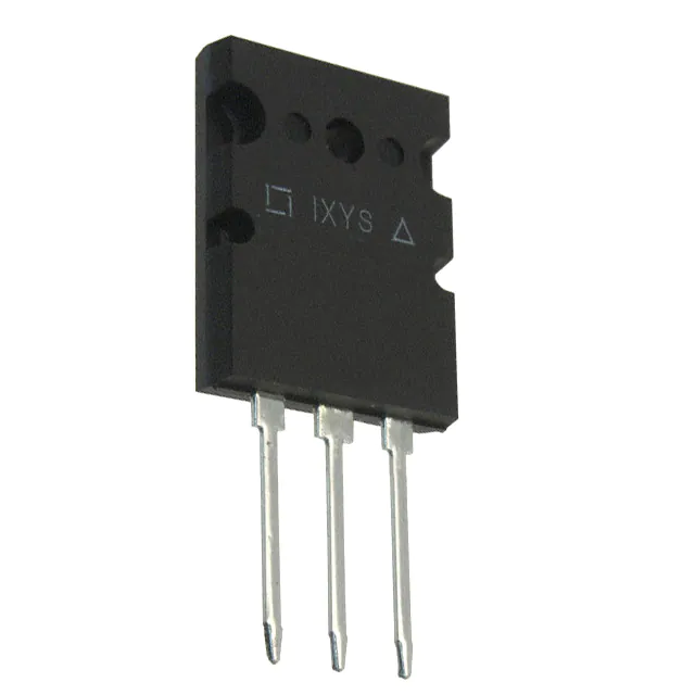
TO-264 (IXTK)
Symbol
Test Conditions
VDSS
TJ = 25°C to 150°C
Maximum Ratings
500
V
VDGR
TJ = 25°C to 150°C; RGS = 1 MΩ
500
V
VGS
Continuous
±30
V
VGSM
Transient
±40
V
ID25
TC = 25°C
IDM
TC = 25°C, pulse width limited by TJM
46
A
100
A
IAR
TC = 25°C
46
A
EAR
TC = 25°C
60
mJ
1.5
J
700
W
-55 to +150
°C
TJM
150
°C
Tstg
-55 to +150
°C
EAS
PD
TC = 25°C
TJ
TL
1.6 mm (0.063 in) from case for 10 s
300
°C
TSOLD
Plastic body for 10 s
260
°C
Md
Fc
Mounting torque
Mounting force
Weight
PLUS247
TO-264
(TO-264)
(PLUS247TM)
1.13/10 Nm/lb.in.
20...120/4.5...27
N/lb.
6
10
g
g
G
D
S
(TAB)
PLUS247 (IXTX)
TAB
G = Gate
S = Source
D = Drain
TAB = Drain
Features
z
z
Designed for linear operation
International standard package
z
Unclamped Inductive switching (UIS)
rated
z
Molding epoxies meet UL 94 V-0
flammability classification
Symbol
Test Conditions
BVDSS
VGS = 0 V, ID = 1 mA
VGS(th)
VDS = VGS, ID = 250 μA
IGSS
VGS = ±30 V, VDS = 0 V
IDSS
VDS = VDSS
VGS = 0 V
RDS(on)
Characteristic Values
(TJ = 25°C, unless otherwise specified)
Min.
Typ.
Max.
500
3
TJ = 25°C
TJ = 125°C
VGS = 20 V, ID = 0.5 ID25, Note 1
Applications
z
V
z
V
z
±200
nA
z
50
1
μA
mA
z
0.16
Ω
6
z
Programmable loads
Current regulators
DC-DC converters
Battery chargers
DC choppers
Temperature and lighting controls
Advantages
z
z
z
Easy to mount
Space savings
High power density
IXYS reserves the right to change limits, test conditions, and dimensions.
© 2007 IXYS CORPORATION, All rights reserved
DS99350A(03/07)
�IXTK46N50L
IXTX46N50L
Symbol
Test Conditions
Characteristic Values
(TJ = 25°C, unless otherwise specified)
Min. Typ. Max.
gfs
VDS = 10 V; ID = 0.5 • ID25, Note 1
7
10
13
S
7000
pF
900
pF
Crss
170
pF
td(on)
40
ns
50
ns
80
ns
42
ns
260
nC
85
nC
125
nC
Ciss
Coss
VGS = 0 V, VDS = 25 V, f = 1 MHz
tr
VGS = 15 V, VDS = 0.5 • VDSS, ID = 0.5 • ID25
td(off)
RG
= 2 Ω (External),
tf
Qg(on)
Qgs
VGS = 15 V, VDS = 0.5 • VDSS, ID = 0.5 • ID25
Qgd
TO-264 (IXTK) Outline
0.18 °C/W
RthJC
RthCS
°C/W
0.15
Safe Operating Area Specification
Symbol
Test Conditions
Min.
SOA
VDS = 400 V, ID = 0.6 A, TC = 90°C
240
Source-Drain Diode
Symbol
Test Conditions
IS
VGS = 0 V
ISM
Typ.
Max.
W
Characteristic Values
(TJ = 25°C, unless otherwise specified)
Min. Typ. Max.
46
A
Repetitive; pulse width limited by TJM
100
A
VSD
IF = IS, VGS = 0 V, Note 1
1.5
V
trr
IF = IS, -di/dt = 100 A/μs, VR = 100V
600
PLUS247TM (IXTX) Outline
ns
Note 1: Pulse test, t < 300 μs, duty cycle, d ≤ 2 %
Terminals: 1 - Gate
2 - Drain (Collector)
3 - Source (Emitter)
4 - Drain (Collector)
Dim.
PRELIMINARY TECHNICAL INFORMATION
The product presented herein is under development. The Technical Specifications offered are
derived from data gathered during objective characterizations of preliminary engineering lots; but
also may yet contain some information supplied during a pre-production design evaluation. IXYS
reserves the right to change limits, test conditions, and dimensions without notice.
A
A1
A2
b
b1
b2
C
D
E
e
L
L1
Q
R
Millimeter
Min. Max.
4.83
5.21
2.29
2.54
1.91
2.16
1.14
1.40
1.91
2.13
2.92
3.12
0.61
0.80
20.80 21.34
15.75 16.13
5.45 BSC
19.81 20.32
3.81
4.32
5.59
6.20
4.32
4.83
Inches
Min. Max.
.190 .205
.090 .100
.075 .085
.045 .055
.075 .084
.115 .123
.024 .031
.819 .840
.620 .635
.215 BSC
.780 .800
.150 .170
.220 0.244
.170 .190
IXYS reserves the right to change limits, test conditions, and dimensions.
IXYS MOSFETs and IGBTs are covered
4,835,592
by one or moreof the following U.S. patents: 4,850,072
4,881,106
4,931,844
5,017,508
5,034,796
5,049,961
5,063,307
5,187,117
5,237,481
5,381,025
5,486,715
6,162,665
6,259,123 B1
6,306,728 B1
6,404,065 B1
6,534,343
6,583,505
6,683,344
6,727,585
7,005,734 B2
6,710,405 B2 6,759,692
7,063,975 B2
6,710,463
6,771,478 B2 7,071,537
7,157,338B2
�IXTK46N50L
IXTX46N50L
Fig. 1. Output Characteristics
@ 25ºC
Fig. 2. Extended Output Characteristics
@ 25ºC
50
100
VGS = 20V
18V
16V
45
40
14V
70
I D - Amperes
12V
30
25
20
15
14V
60
50
40
12V
30
10V
10
20
9V
8V
7V
5
0
0
1
2
3
4
5
6
7
10V
9V
8V
10
0
8
9
0
3
6
9
Fig. 3. Output Characteristics
@ 125ºC
21
24
27
30
VGS = 20V
2.8
14V
R D S (on) - Normalized
I D - Amperes
18
3.1
VGS = 20V
18V
16V
40
15
Fig. 4. RDS(on) Norm alized to 0.5 ID25 Value
vs. Junction Tem perature
50
45
12
V D S - Volts
V D S - Volts
35
12V
30
25
20
10V
15
9V
8V
7V
5
0
2.5
2.2
I D = 46A
1.9
1.6
I D = 23A
1.3
1.0
10
0.7
0.4
0
2
4
6
8
10
12
14
16
18
-50
-25
V D S - Volts
0
25
50
75
100
125
150
TJ - Degrees Centigrade
Fig. 5. RDS(on) Norm alized to
0.5 ID25 Value vs. ID
Fig. 6. Drain Current vs. Case
Tem perature
3.0
50
2.8
VGS = 20V
45
2.6
40
TJ = 125ºC
2.4
35
I D - Amperes
R D S (on) - Normalized
16V
80
35
I D - Amperes
VGS = 20V
18V
90
2.2
2.0
1.8
1.6
30
25
20
15
1.4
10
1.2
TJ = 25ºC
1.0
5
0.8
0
0
20
40
60
80
I D - Amperes
© 2007 IXYS CORPORATION, All rights reserved
100
120
-50
-25
0
25
50
75
100
TC - Degrees Centigrade
125
150
�IXTK46N50L
IXTX46N50L
Fig. 8. Trans conductance
Fig. 7. Input Adm ittance
20
70
18
60
16
14
g f s - Siemens
I D - Amperes
50
40
30
TJ = 125ºC
25ºC
-40ºC
20
10
TJ = -40ºC
25ºC
125ºC
12
10
8
6
4
2
0
0
5
6
7
8
9
10
11
12
13
14
15
0
10
20
30
V G S - Volts
Fig. 9. Source Current vs .
Source -To-Drain Voltage
16
60
14
VG S - Volts
I S - Amperes
60
70
VDS = 250V
I D = 23A
I G = 10mA
12
50
40
TJ = 125ºC
TJ = 25ºC
20
10
8
6
4
10
2
0
0
0.5
0.6
0.7
0.8
0.9
1
V S D - Volts
10000
C iss
C oss
1000
C rss
f = 1MHz
100
0
5
10
15
20
25
0
30
60
90
120
150
180
Q G - nanoCoulombs
Fig. 11. Capacitance
Capacitance - pF
50
Fig. 10. Gate Charge
70
30
40
I D - Amperes
30
35
40
V D S - Volts
IXYS reserves the right to change limits, test conditions, and dimensions.
210
240
270
�IXTK46N50L
IXTX46N50L
Fig. 12. Forw ard-Bias Safe
Fig. 13. Forw ard-Bias Safe
Operating Area @ T C = 25ºC
Operating Area @ T C = 90ºC
1000
1000
TJ = 150ºC
TJ = 150ºC
R DS(on) Limit
R DS(on) Limit
100
25µs
100µs
10
1ms
I D - Amperes
I D - Amperes
100
25µs
100µs
10
1ms
10ms
DC
1
10ms
1
DC
0.1
0.1
10
100
1000
10
100
1000
V D S - Volts
V D S - Volts
Fig. 14. Maxim um Transient Therm al Im pedance
Z (th) J C - (ºC/W)
1.000
0.100
0.010
0.001
0.1
1
10
100
1000
Pulse Width - milliseconds
© 2007 IXYS CORPORATION, All rights reserved
IXYS REF: T_46N50L (8N) 4-05-07-A.xls
�Disclaimer Notice - Information furnished is believed to be accurate and reliable. However, users should independently
evaluate the suitability of and test each product selected for their own applications. Littelfuse products are not designed for,
and may not be used in, all applications.Read complete Disclaimer Notice at www.littelfuse.com/disclaimer-electronics.
�


 工商网监
湘ICP备2023018690号
工商网监
湘ICP备2023018690号
