PolarHTTM
Power MOSFET
IXTH 88N30P
IXTK 88N30P
IXTQ 88N30P
IXTT 88N30P
VDSS
ID25
RDS(on)
N-Channel Enhancement Mode
Avalanche Rated
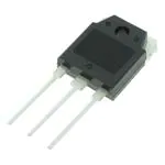
TO-247 (IXTH)
Symbol
Test Conditions
VDSS
TJ = 25° C to 150° C
300
V
Maximum Ratings
VDGR
TJ = 25° C to 150° C; RGS = 1 MΩ
300
V
VGS
Continuous
±20
V
VGSM
Transient
±30
V
ID25
TC = 25° C
88
A
ID(RMS)
External lead current limit
75
A
IDM
TC = 25° C, pulse width limited by TJM
220
A
IAR
TC = 25° C
60
A
EAR
TC = 25° C
60
mJ
EAS
TC = 25° C
2.0
J
dv/dt
IS ≤ IDM, di/dt ≤ 100 A/µs, VDD ≤ VDSS
TJ ≤150° C, RG = 4 Ω
10
V/ns
PD
TC = 25° C
600
W
-55 ... +150
150
-55 ... +150
°C
°C
°C
300
260
°C
°C
G
TJ
TJM
Tstg
TL
TSOLD
1.6 mm (0.062 in.) from case for 10 s
Plastic body for 10 s
Md
Mounting torque
Weight
TO-247
TO-264
TO-3P & TO-268
D
D (TAB)
S
TO-264 (IXTK)
G
D
S
D (TAB)
TO-3P (IXTQ)
G
D
(TAB)
S
TO-268 (IXTT)
1.13/10 Nm/lb.in.
6.0
10
5.5
Symbol
Test Conditions
(TJ = 25° C, unless otherwise specified)
g
g
g
Characteristic Values
Min. Typ.
Max.
BVDSS
VGS = 0 V, ID = 250 µA
300
VGS(th)
VDS = VGS, ID = 250µA
2.5
IGSS
VGS = ±20 VDC, VDS = 0
IDSS
VDS = VDSS
VGS = 0 V
RDS(on)
VGS = 10 V, ID = 0.5 ID25
Pulse test, t ≤300 µs, duty cycle d ≤ 2 %
© 2006 IXYS All rights reserved
= 300 V
= 88 A
≤ 40 mΩ
Ω
TJ = 125° C
V
5.0
V
±100
nA
100
1
µA
mA
40
mΩ
G
G = Gate
S = Source
S
D (TAB)
D = Drain
TAB = Drain
Features
l
International standard package
l
Unclamped Inductive Switching (UIS)
rated
l
Low package inductance
- easy to drive and to protect
Advantages
l
Easy to mount
l
Space savings
l
High power density
DS99129E(12/05)
�IXTH 88N30P IXTK 88N30P
IXTQ 88N30P IXTT 88N30P
Symbol
Test Conditions
Characteristic Values
(TJ = 25° C unless otherwise specified)
Min.
Typ.
Max.
gfs
VDS= 10 V; ID = 0.5 ID25, pulse test
45
60
S
6300
pF
950
pF
Crss
190
pF
td(on)
25
ns
Ciss
VGS = 0 V, VDS = 25 V, f = 1 MHz
Coss
tr
VGS = 10 V, VDS = 0.5 VDSS, ID = 60 A
24
ns
td(off)
RG = 3.3 Ω (External)
96
ns
25
ns
180
nC
44
nC
90
nC
tf
Qg(on)
VGS= 10 V, VDS = 0.5 VDSS, ID = 0.5 ID25
Qgs
Qgd
RthJC
0.21° C/W
TO-247 and TO-3P
TO-264
RthCS
RthCS
° C/W
° C/W
0.21
0.15
Source-Drain Diode
Characteristic Values
(TJ = 25° C, unless otherwise specified)
Min.
Typ.
Max.
Symbol
Test Conditions
IS
VGS = 0 V
88
A
ISM
Repetitive
220
A
VSD
IF = IS, VGS = 0 V,
Pulse test, t ≤ 300 µs, duty cycle d ≤ 2 %
1.5
V
trr
QRM
IF = 25 A, -di/dt = 100 A/µs
VR = 100 V, VGS = 0 V
250
3.3
ns
µC
Characteristic Curves
Fig. 2. Extended Output Characteristics
@ 25ºC
Fig. 1. Output Characteristics
@ 25ºC
200
90
VGS = 10V
9V
8V
80
9V
160
140
60
I D - Amperes
I D - Amperes
70
VGS = 10V
180
50
7V
40
30
20
6V
5V
1
1.5
7V
100
80
60
6V
20
5V
0
0
0.5
120
40
10
0
8V
2
2.5
3
3.5
4
0
2
4
6
8
10
12
14
16
V D S - Volts
V D S - Volts
IXYS reserves the right to change limits, test conditions, and dimensions.
IXYS MOSFETs and IGBTs are covered by 4,835,592
one or moreof the following U.S. patents: 4,850,072
4,881,106
4,931,844
5,017,508
5,034,796
5,049,961
5,063,307
5,187,117
5,237,481
5,381,025
5,486,715
6,162,665
6,259,123 B1
6,306,728 B1
6,404,065 B1
6,534,343
6,583,505
6,683,344
6,710,405B2
6,710,463
6,727,585
6,759,692
6771478 B2
18
20
�IXTH 88N30P IXTK 88N30P
IXTQ 88N30P IXTT 88N30P
Fig. 3. Output Char acte r is tics
@ 125ºC
Fig. 4. RDS(on ) Nor m alize d to 0.5 ID25
V alue vs . Junction Te m pe r atur e
90
3
V GS = 10V
9V
8V
I D - Amperes
70
V GS = 10V
2.6
R D S (on) - Normalized
80
2.8
7V
60
50
40
6V
30
20
2.2
2
1.8
I D = 88A
1.6
1.4
I D = 44A
1.2
1
0.8
5V
10
2.4
0.6
0
0.4
0
1
2
3
4
5
6
7
8
9
-50
V D S - V olts
-25
125
150
70
2.8
2.6
TJ = 125ºC
I D - Amperes
R D S (on) - Normalized
100
External Lead C urrent Lim it
80
2.4
2.2
2
1.8
1.6
1.4
60
50
40
30
20
1.2
TJ = 25ºC
10
1
0
0.8
0
20
40
60
80
-50
100 120 140 160 180 200
I D - A mperes
-25
0
25
50
75
100
TC - Degrees Centigrade
125
150
Fig. 8. Transconductance
Fig. 7. Input Adm ittance
100
160
90
140
TJ = -40ºC
25ºC
125ºC
80
g f s - Siemens
120
I D - Amperes
75
90
V GS = 10V
3
50
Fig. 6. Dr ain Cur r e nt vs . Cas e
Te m pe r atur e
0.5 ID25 V alue vs . ID
3.2
25
TJ - Degrees Centigrade
Fig. 5. RDS(on) Nor m alize d to
3.4
0
100
80
60
TJ = 125ºC
25ºC
-40ºC
40
20
70
60
50
40
30
20
10
0
0
4
4.5
5
5.5
6
6.5
V G S - Volts
© 2006 IXYS All rights reserved
7
7.5
8
0
20
40
60
80
100
120
I D - Amperes
140
160
180
�IXTH 88N30P IXTK 88N30P
IXTQ 88N30P IXTT 88N30P
Fig. 9. Source Current vs.
Source-To-Drain Voltage
Fig. 10. Gate Charge
10
280
240
VDS = 150V
8
I D = 44A
I G = 10mA
7
VG S - Volts
I S - Amperes
200
9
160
120
TJ = 125ºC
80
6
5
4
3
2
TJ = 25ºC
40
1
0
0
0.4
0.6
0.8
1
V S D - Volts
1.2
1.4
0
1.6
20
40
60
80
100
120
140
160
180
Q G - nanoCoulombs
Fig. 12. Forw ard-Bias
Safe Operating Area
Fig. 11. Capacitance
10000
1000
C iss
I D - Amperes
Capacitance - picoFarads
TJ = 150ºC
R DS(on) Limit
C oss
1000
TC = 25ºC
100
100µs
25µs
1ms
10ms
10
DC
C rss
f = 1MHz
100
1
0
5
10
15
20
25
V D S - Volts
30
35
40
10
100
1000
V D S - Volts
Fig. 13. Maximum Transient Thermal Resistance
R(th) J C - ºC / W
1.00
0.10
0.01
1
10
100
Pulse Width - milliseconds
IXYS reserves the right to change limits, test conditions, and dimensions.
1000
�IXTH 88N30P IXTK 88N30P
IXTQ 88N30P IXTT 88N30P
TO-247 (IXTH) Outline
1
2
TO-268 (IXTT) Outline
3
Terminals:
1. Gate
2,4. Drain
3. Source
Dim.
TO-3P (IXTQ) Outline
Millimeter
Min. Max.
A
4.7
5.3
2.2
2.54
A1
A2
2.2
2.6
b
1.0
1.4
1.65
2.13
b1
b2
2.87
3.12
C
.4
.8
D
20.80 21.46
E
15.75 16.26
e
5.20
5.72
L
19.81 20.32
L1
4.50
∅P 3.55
3.65
Q
5.89
6.40
R
4.32
5.49
S
6.15 BSC
Inches
Min. Max.
.185 .209
.087 .102
.059 .098
.040 .055
.065 .084
.113 .123
.016 .031
.819 .845
.610 .640
0.205 0.225
.780 .800
.177
.140 .144
0.232 0.252
.170 .216
242 BSC
TO-264 (IXTK) Outline
© 2006 IXYS All rights reserved
Terminals:
1. Gate
2,4. Drain
3. Source
�Disclaimer Notice - Information furnished is believed to be accurate and reliable. However, users should independently
evaluate the suitability of and test each product selected for their own applications. Littelfuse products are not designed for,
and may not be used in, all applications.Read complete Disclaimer Notice at www.littelfuse.com/disclaimer-electronics.
�


 工商网监
湘ICP备2023018690号
工商网监
湘ICP备2023018690号

