JIANGSU CHANGJING ELECTRONICS TECHNOLOGY CO., LTD
100mA Fixed Output Three Terminal Positive Regulators
CJ78L Series
1
Three Terminal Positive Regulators
Introduction
The CJ78L series is a group of three-terminal positive
voltage linear regulators with a fixed voltage output. It
can support a maximum input voltage of 30V (or 35V)
and provide an output current of 100mA with good
heat dissipation. The CJ78L series eliminates the
need for peripheral resistors to define voltage outputs,
which improves the space efficiency of printed circuit
boards (PCBs). In addition, the CJ78L series
integrates internal current limiting, short-circuit
protection, and thermal shutdown, making it virtually
unaffected by overload. Therefore, the CJ78L series
is widely used in a variety of scenarios, such as card
monitoring, to eliminate noise and distribution issues
related to single-point monitoring. When used as an
alternative to the Zener diode-resistor combination,
the CJ78L series can effectively increase the output
impedance and reduce the bias current.
2
•
Available Output Voltage:
5.0V, 6.0V, 8.0V, 9.0V, 12V and 15V
Maximum Input Voltage:
30V for VOUT < 10V products
35V for VOUT > 10V products
•
•
PACKAGE
Maximum Output Current:
Exceed 100mA at TJ = 25°C
Output Tolerances at TJ = 25°C:
•
•
•
•
±3% for Conventional Device
±2% can be Customized
Output Tolerances of ±5% over the
Operating Junction Temperature
Build-in Current Limit
Short Circuit Protection
Thermal Shutdown Protection
No External Components
4
Applications
•
•
•
•
TV Board
Air Conditioner
Vehicle Mounted Radar
Charging Device
•
SOT-23-3L
CJ78L Series
Features
•
Available Packages
PART NUMBER
3
SOT-89-3L
TO-92
Note: For all available packages, please refer to the part
Orderable Information.
INPUT
CIN
0.33µF
IN
CJ78L Series
OUT
GND
OUTPUT
COUT
0.1µF
Typical Application Circuit
Please carefully read the notice at the end of this data sheet about product use, data sheet changes and important statements.
�CJ78L Series
5
Orderable Information
MODEL
DEVICE
PACKAGE
OP TJ
ECO PLAN
MSL
PACKING OPTION
RoHS &
Level 3
Tape and Reel
Green
168 HR
3000 Units / Reel
RoHS &
Level 3
Tape and Reel
Green
168 HR
1000 Units / Reel
RoHS &
Level 3
Tape and Reel
Green
168 HR
1000 Units / Reel
RoHS &
Level 3
Tape and Reel
Green
168 HR
1000 Units / Reel
RoHS &
Level 3
Tape and Reel
Green
168 HR
1000 Units / Reel
RoHS &
Level 3
Tape and Reel
Green
168 HR
1000 Units / Reel
RoHS &
Level 3
Tape and Reel
Green
168 HR
1000 Units / Reel
RoHS &
Level 3
Bulk
Green
168 HR
1000 Units / Bag
RoHS &
Level 3
Bulk
Green
168 HR
1000 Units / Bag
RoHS &
Level 3
Bulk
Green
168 HR
1000 Units / Bag
RoHS &
Level 3
Bulk
Green
168 HR
1000 Units / Bag
RoHS &
Level 3
Bulk
Green
168 HR
1000 Units / Bag
RoHS &
Level 3
Bulk
Green
168 HR
1000 Units / Bag
SORT
Conventional Products (±3% grade)
CJ78L-5.0
CJ78L05
SOT-23-3L
-40 ~ 125°C
CJ78L-5.0
CJ78L05
SOT-89-3L
-40 ~ 125°C
CJ78L-6.0
CJ78L06
SOT-89-3L
-40 ~ 125°C
CJ78L-8.0
CJ78L08
SOT-89-3L
-40 ~ 125°C
CJ78L-9.0
CJ78L09
SOT-89-3L
-40 ~ 125°C
CJ78L-12
CJ78L12
SOT-89-3L
-40 ~ 125°C
CJ78L-15
CJ78L15
SOT-89-3L
-40 ~ 125°C
CJ78L-5.0
CJ78L05
TO-92
-40 ~ 125°C
CJ78L-6.0
CJ78L06
TO-92
-40 ~ 125°C
CJ78L-8.0
CJ78L08
TO-92
-40 ~ 125°C
CJ78L-9.0
CJ78L09
TO-92
-40 ~ 125°C
CJ78L-12
CJ78L12
TO-92
-40 ~ 125°C
CJ78L-15
CJ78L15
TO-92
-40 ~ 125°C
www.jscj-elec.com
2
Active
Active
Active
Active
Active
Active
Active
Active
Active
Active
Active
Active
Active
Rev. - 3.2
�CJ78L Series
5
Orderable Information
MODEL
DEVICE
PACKAGE
OP TJ
ECO PLAN
MSL
PACKING OPTION
SORT
Conventional Products (±3% grade, continued)
CJ78L-5.0
CJ78L05-TA
TO-92
-40 ~ 125°C
CJ78L-6.0
CJ78L06-TA
TO-92
-40 ~ 125°C
CJ78L-8.0
CJ78L08-TA
TO-92
-40 ~ 125°C
CJ78L-9.0
CJ78L09-TA
TO-92
-40 ~ 125°C
CJ78L-12
CJ78L12-TA
TO-92
-40 ~ 125°C
CJ78L-15
CJ78L15-TA
TO-92
-40 ~ 125°C
RoHS &
Level 3
Ammo
Green
168 HR
2000 Units / Box
RoHS &
Level 3
Ammo
Green
168 HR
2000 Units / Box
RoHS &
Level 3
Ammo
Green
168 HR
2000 Units / Box
RoHS &
Level 3
Ammo
Green
168 HR
2000 Units / Box
RoHS &
Level 3
Ammo
Green
168 HR
2000 Units / Box
RoHS &
Level 3
Ammo
Green
168 HR
2000 Units / Box
RoHS &
Level 3
Tape and Reel
Green
168 HR
3000 Units / Reel
RoHS &
Level 3
Tape and Reel
Green
168 HR
3000 Units / Reel
RoHS &
Level 3
Tape and Reel
Green
168 HR
1000 Units / Reel
RoHS &
Level 3
Bulk
Green
168 HR
1000 Units / Bag
RoHS &
Level 3
Ammo
Green
168 HR
2000 Units / Box
-
-
-
Active
Active
Active
Active
Active
Active
Customized Products
CJ78L-x.x
CJ78Lxx
SOT-23-3L
-40 ~ 125°C
-
SOT-23-3L
-40 ~ 125°C
-
SOT-89-3L
-40 ~ 125°C
-
TO-92
-40 ~ 125°C
-
TO-92
-40 ~ 125°C
-
-
-
CJ78L-x.x
±2% grade
Others
Customized
Customized
Customized
Customized
Customized
Customized
Note:
ECO PLAN: For the RoHS and Green certification standards of this product, please refer to the official
report provided by JSCJ.
MSL: Moisture Sensitivity Level. Determined according to JEDEC industry standard classification.
SORT: Specifically defined as follows:
Active: Recommended for new products;
Customized: Products manufactured to meet the specific needs of customers;
Preview: The device has been released and has not been fully mass produced. The sample may or may not
be available;
NoRD: It is not recommended to use the device for new design. The device is only produced for the needs of
existing customers;
Obsolete: The device has been discontinued.
www.jscj-elec.com
3
Rev. - 3.2
�CJ78L Series
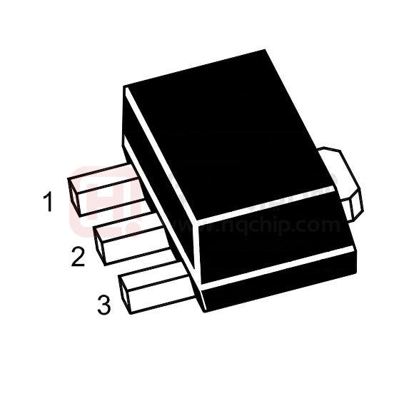
6
Pin Configuration and Marking Information
6.1 Pin Configuration and Function
SOT-23-3L
SOT-89-3L
TO-92
G
O
I
O
G
O G I
I
Figure 5-1. Package Top View
CJ78L Series
PIN
I/O
DESCRIPTION
NAME
SOT-23-3L
SOT-89-3L
TO-92
IN
2
3
3
I
Input to the device.
GND
3
2
2
-
Regulator ground.
OUT
1
1
1
O
Output of the regulator.
6.2 Marking Information
78LXX
CJ
78LXX
CJ
78LXX
YYY
O G
I
"78LXX" or "CJ78LXX": Product number, the "XX" in the "78LXX" or "CJ78LXX" represents the output voltage, for
example, if VOUT = 5.0V, "XX" is "05".
" " Solid dot: Lower left, represents green molding compound device. Upper right, anchor point.
"YYY": Code.
www.jscj-elec.com
4
Rev. - 3.2
�CJ78L Series
7
Specifications
7.1 Absolute Maximum Ratings
(over operating free-air temperature range, unless otherwise specified)
CHARACTERISTIC
SYMBOL
VALUE
UNIT
CJ78L05
CJ78L06
30
CJ78L08
Maximum input voltage(2)
VIN MAX
CJ78L09
V
CJ78L12
35
CJ78L15
SOT-23-3L
Maximum power dissipation
SOT-89-3L
PD Max
Internally Limited(3)
W
Maximum junction temperature
TJ Max
150
°C
Storage temperature range
Tstg
- 65 ~ 150
°C
Soldering temperature & time
Tsolder
260°C, 10s
-
TO-92
(1) Stresses beyond those listed under Absolute Maximum Ratings may cause permanent damage to the device. These are
stress ratings only, which do not imply functional operation of the device at these or any other conditions beyond those indicated
under Recommended Operating Conditions. Exposure to absolute-maximum rated conditions for extended periods may affect
device reliability.
(2) All voltages are with respect to network ground terminal.
(3) Refer to Thermal Information for details.
7.2 Recommended Operating Conditions
PARAMETER
SYMBOL
MIN.
NOM.
MAX.
UNIT
Operating junction temperature
TJ
-40
-
125
°C
Operating ambient temperature
TA
-
-
-
°C
SYMBOL
VALUE
UNIT
Human body model
VESD-HBM
2000
Machine model
VESD-MM
400
7.3 ESD Ratings
ESD RATINGS
Electrostatic discharge(4)
V
(4) ESD testing is conducted in accordance with the relevant specifications formulated by the Joint Electronic Equipment
Engineering Commission (JEDEC). The human body mode (HBM) electrostatic discharge test is based on the JESD22-114D
test standard, using a 100pF capacitor and discharging to each pin of the device through a resistance of 1.5kΩ. The
electrostatic discharge test in mechanical mode (MM) is based on the JESD22-115-A test standard and uses a 200pF capacitor
to discharge directly to each pin of the device.
www.jscj-elec.com
5
Rev. - 3.2
�CJ78L Series
7
Specifications
7.4 Thermal Information
THERMAL METRIC(5)
SYMBOL
Junction-to-ambient thermal resistance
Junction-to-case thermal resistance
Reference maximum power
dissipation for continuous operation
CJ78L Series
UNIT
SOT-23-3L
SOT-89-3L
TO-92
RΘJA
257.1
116.5
178.2
°C/W
RΘJC
63.8
29.1
42.2
°C/W
PD Ref
0.38
0.83
0.56
W
(5) Thermal metric is measured in still air with TA = 25°C and installed on a 1 in2 FR-4 board covered with 2 ounces of copper.
7.5 Electrical Characteristics
CJ78L05 (VIN = 10V, IOUT = 40mA, CIN = 0.33μF, COUT = 0.1μF, TJ = 25°C, unless otherwise specified)
CHARACTERISTIC
SYMBOL
Input voltage
VIN
TEST CONDITIONS(6)
TJ = 25°C
Output voltage
VOUT
Output current
IOUT
Quiescent current
IQ
Quiescent current
change
∆IQ
TYP.
MAX.
UNIT
-
-
30
V
±3% grade(7)
4.85
±2% grade(7)
4.90
5.15
5.00
5.10
4.75
IOUT = 1 to 70mA
4.75
-
100
-
-
mA
IOUT = 0mA
-
3.8
6.0
mA
VIN = 8 to 20V
-
-
1.5
mA
IOUT = 1 to 40mA
-
-
0.1
mA
-
-
1.7
-
V
VIN = 7 to 20V
-
32
150
VIN = 8 to 20V
-
26
100
IOUT = 1 to 100mA
-
15
60
IOUT = 1 to 40mA
-
8
30
-
42
-
µV/VOUT
41
49
-
dB
VDO(8)
Line regulation
ΔVLINE
Load regulation
ΔVLOAD
Output noise voltage
VN
f = 10 to 100kHz
Ripple rejection
RR
VIN = 8 to 20V, f = 120Hz
6
5.25
V
VIN = 7 to 20V, IOUT = 1 to 40mA
Dropout voltage
www.jscj-elec.com
MIN.
5.25
mV
mV
Rev. - 3.2
�CJ78L Series
7
Specifications
7.5 Electrical Characteristics (continued)
CJ78L06 (VIN = 11V, IOUT = 40mA, CIN = 0.33μF, COUT = 0.1μF, TJ = 25°C, unless otherwise specified)
CHARACTERISTIC
SYMBOL
Input voltage
VIN
TEST CONDITIONS(6)
TJ = 25°C
Output voltage
VOUT
Output current
IOUT
Quiescent current
IQ
Quiescent current
change
∆IQ
MIN.
TYP.
MAX.
UNIT
-
-
30
V
±3% grade(7)
5.82
±2% grade(7)
5.88
6.18
6.00
6.12
5.70
IOUT = 1 to 70mA
5.70
-
100
-
-
mA
IOUT = 0mA
-
3.9
6.0
mA
VIN = 9 to 20V
-
-
1.5
mA
IOUT = 1 to 40mA
-
-
0.1
mA
-
-
1.7
-
V
VIN = 8 to 20V
-
35
175
VIN = 9 to 20V
-
29
125
IOUT = 1 to 100mA
-
16
80
IOUT = 1 to 40mA,
-
9
40
-
46
-
µV/VOUT
40
48
-
dB
Dropout voltage
VDO(8)
Line regulation
ΔVLINE
Load regulation
ΔVLOAD
Output noise voltage
VN
f = 10 to 100kHz
Ripple rejection
RR
VIN = 9 to 19V, f = 120Hz
6.30
V
VIN = 8 to 20V, IOUT = 1 to 40mA
6.30
mV
mV
CJ78L08 (VIN = 14V, IOUT = 40mA, CIN = 0.33μF, COUT = 0.1μF, TJ = 25°C, unless otherwise specified)
CHARACTERISTIC
SYMBOL
Input voltage
VIN
TEST CONDITIONS(6)
TJ = 25°C
Output voltage
VOUT
Output current
IOUT
Quiescent current
IQ
Quiescent current
change
∆IQ
TYP.
MAX.
UNIT
-
-
30
V
±3% grade(7)
7.76
±2% grade(7)
7.84
8.24
8.00
8.15
7.60
IOUT = 1 to 70mA
7.76
-
100
-
-
mA
IOUT = 0mA
-
4.0
6.0
mA
VIN = 11 to 23V
-
-
1.5
mA
IOUT = 1 to 40mA
-
-
0.1
mA
-
-
1.7
-
V
VIN = 10.5 to 23V
-
42
175
VIN = 11 to 23V
-
36
125
IOUT = 1 to 100mA
-
18
80
IOUT = 1 to 40mA
-
10
40
-
54
-
µV/VOUT
37
46
-
dB
VDO(8)
Line regulation
ΔVLINE
Load regulation
ΔVLOAD
Output noise voltage
VN
f = 10 to 100kHz
Ripple rejection
RR
VIN = 13 to 23V, f = 120Hz
7
8.40
V
VIN = 10.5 to 23V, IOUT = 1 to 40mA
Dropout voltage
www.jscj-elec.com
MIN.
8.40
mV
mV
Rev. - 3.2
�CJ78L Series
7
Specifications
7.5 Electrical Characteristics (continued)
CJ78L09 (VIN = 16V, IOUT = 40mA, CIN = 0.33μF, COUT = 0.1μF, TJ = 25°C, unless otherwise specified)
CHARACTERISTIC
SYMBOL
Input voltage
VIN
TEST CONDITIONS(6)
TJ = 25°C
Output voltage
VOUT
Output current
IOUT
Quiescent current
IQ
Quiescent current
change
∆IQ
MIN.
TYP.
MAX.
UNIT
-
-
30
V
±3% grade(7)
8.73
±2% grade(7)
8.82
9.27
9.00
9.18
8.55
IOUT = 1 to 70mA
8.55
-
100
-
-
mA
IOUT = 0mA
-
4.1
6.0
mA
VIN = 13 to 24V
-
-
1.5
mA
IOUT = 1 to 40mA
-
-
0.1
mA
-
-
1.7
-
V
VIN = 12 to 24V
-
45
175
VIN = 13 to 24V
-
40
125
IOUT = 1 to 100mA
-
19
90
IOUT = 1 to 40mA
-
11
40
-
58
-
µV/VOUT
37
45
-
dB
Dropout voltage
VDO(8)
Line regulation
ΔVLINE
Load regulation
ΔVLOAD
Output noise voltage
VN
f = 10 to 100kHz
Ripple rejection
RR
VIN = 15 to 25V, f = 120Hz
9.45
V
VIN = 12 to 24V, IOUT = 1 to 40mA
9.45
mV
mV
CJ78L12 (VIN = 19V, IOUT = 40mA, CIN = 0.33μF, COUT = 0.1μF, TJ = 25°C, unless otherwise specified)
CHARACTERISTIC
SYMBOL
Input voltage
VIN
TEST CONDITIONS(6)
TJ = 25°C
Output voltage
VOUT
Output current
IOUT
Quiescent current
IQ
Quiescent current
change
∆IQ
TYP.
MAX.
UNIT
-
-
35
V
±3% grade(7)
11.64
±2% grade(7)
11.76
VIN = 14 to 27V, IOUT = 1 to 40mA
11.40
IOUT = 1 to 70mA
11.40
-
12.36
12.00
12.24
12.60
V
12.60
100
-
-
mA
IOUT = 0mA
-
4.3
6.5
mA
VIN = 14.5 to 27V
-
-
1.5
mA
IOUT = 1 to 40mA
-
-
0.1
mA
-
-
1.7
-
V
VIN = 14.5 to 27V
-
55
250
VIN = 16 to 27V
-
49
200
IOUT = 1 to 100mA
-
22
100
IOUT = 1 to 40mA
-
13
50
-
70
-
µV/VOUT
37
42
-
dB
Dropout voltage
VDO(8)
Line regulation
ΔVLINE
Load regulation
ΔVLOAD
Output noise voltage
VN
f = 10 to 100kHz
Ripple rejection
RR
VIN = 15 to 25V, f = 120Hz
www.jscj-elec.com
MIN.
8
mV
mV
Rev. - 3.2
�CJ78L Series
7
Specifications
7.5 Electrical Characteristics (continued)
CJ78L15 (VIN = 23V, IOUT = 40mA, CIN = 0.33μF, COUT = 0.1μF, TJ = 25°C, unless otherwise specified)
CHARACTERISTIC
SYMBOL
Input voltage
VIN
TEST CONDITIONS(6)
TJ = 25°C
Output voltage
VOUT
Output current
IOUT
Quiescent current
IQ
Quiescent current
change
∆IQ
MIN.
TYP.
MAX.
UNIT
-
-
35
V
±3% grade(7)
14.55
±2% grade(7)
14.70
VIN = 17.5 to 30V, IOUT = 1 to 40mA
14.25
IOUT = 1 to 70mA
14.25
-
15.45
15.00
15.30
V
15.75
15.75
100
-
-
mA
IOUT = 0mA
-
4.6
6.5
mA
VIN = 19 to 30V
-
-
1.5
mA
IOUT = 1 to 40mA
-
-
0.1
mA
-
-
1.7
-
V
VIN = 17.5 to 30V
-
65
300
VIN = 19 to 30V
-
58
250
IOUT = 1 to 100mA
-
25
150
IOUT = 1 to 40mA
-
15
75
-
82
-
µV/VOUT
34
39
-
dB
Dropout voltage
VDO(8)
Line regulation
ΔVLINE
Load regulation
ΔVLOAD
Output noise voltage
VN
f = 10 to 100kHz
Ripple rejection
RR
VIN = 18.5 to 28.5V, f = 120Hz
mV
mV
(6) Pulse test technology is used to make TJ as close to TA as possible. Thermal effects must be considered separately.
(7) Output voltage tolerances of ±3% for conventional device, ±2% can be customized.
(8) Test the difference of output voltage and input voltage when input voltage is decreased gradually till output voltage equals to
95% of VOUT.
www.jscj-elec.com
9
Rev. - 3.2
�CJ78L Series
Specifications
7.6 Typical Characteristics
CJ78L05 (VOUT = 5.0V, TJ = 25°C, unless otherwise specified)
Output Characteristics
7
Dropout Characteristics
6.0
IO=0mA
A
=4
0m
I
O
A
=1
00
m
I
O
3.5
A
=7
0m
3.0
I
O
2
4.0
A
3
4.5
=0
m
4
5.0
I
VO
5
O
(V)
5.5
OUTPUT VOLTAGE
(V)
OUTPUT VOLTAGE VO
TJ=25℃
TJ=25℃
6
1
0
2.5
0
5
10
15
20
INPUT VOLTAGE
VIN
25
6
7
8
VIN
10
9
(V)
Current Cut-off Grid Voltage
7
IO=0mA
VIN=10V
TJ=25℃
TJ=25℃
(V)
6
Pulsed
5
VO
IQ
2.5
OUTPUT VOLTAGE
QUIESCENT CURRENT
5
INPUT VOLTAGE
3.0
2.0
1.5
1.0
4
3
2
1
0.5
0.0
4
(V)
3.5
(mA)
2.0
30
Quiescent Current vs Input Voltage
4.0
0
5
10
15
20
INPUT VOLTAGE
VIN
25
0
0.00
30
0.05
0.10
0.15
OUTPUT CURRENT
(V)
Output Voltage vs Junction Temperature
6.0
IO
0.20
0.25
(A)
Power Derating Curve
300
Vin=10V
(mW)
5.5
POWER DISSIPATION
PD
(V)
IO=5mA
OUTPUT VOLTAGE VO
7
5.0
4.5
4.0
-40
-25
0
25
50
JUNCTION TEMPERATURE
www.jscj-elec.com
75
TJ
100
250
200
150
100
50
0
-40
125
(℃ )
-25
0
25
50
JUNCTION TEMPERATURE
10
75
TJ
100
125
(℃ )
Rev. - 3.2
�CJ78L Series
Specifications
7.6 Typical Characteristics (continued)
CJ78L06 (VOUT = 6.0V, TJ = 25°C, unless otherwise specified)
Dropout Characteristics
Output Characteristics
8
6.5
TJ=25ć
IO=0mA
6.0
(V)
A
5.5
I
O
VO
=4
0m
6
5.0
0
5
10
15
20
INPUT VOLTAGE
VIN
25
7
8
IO=0mA
10
9
VIN
(V)
Current Cut-off Grid Voltage
7
VIN=11V
TJ=25ć
6
Pulsed
(V)
4
VO
IQ
(mA)
6
INPUT VOLTAGE
TJ=25ć
3
OUTPUT VOLTAGE
QUIESCENT CURRENT
5
(V)
Quiescent Current
5
A
I
O
A
3.0
30
I
O
3.5
0
=1
00
m
=0
m
I
4.0
=7
0m
2
4.5
O
4
A
OUTPUT VOLTAGE
OUTPUT VOLTAGE VO
(V)
TJ=25ć
2
1
0
0
5
10
15
20
INPUT VOLTAGE
VIN
25
5
4
3
2
1
0.00
30
0.05
0.10
0.15
0.20
OUTPUT CURRENT
(V)
Output Voltage vs Junction Temperature
IO
0.25
0.30
(A)
Power Derating Curve
750
8
Vin= 11V
POWER DISSIPATION PD (mW)
IO= 5mA
7
OUTPUT VOLTAGE VO (V)
7
6
5
4
500
375
250
125
3
2
-40
625
-25
www.jscj-elec.com
0
25
50
75
JUNCTION TEMPERATURE TJ (℃ )
100
0
125
-40
-25
0
25
50
75
100
125
JUNCTION TEMPERATURE TJ (℃ )
11
Rev. - 3.2
�CJ78L Series
Specifications
7.6 Typical Characteristics (continued)
CJ78L08 (VOUT = 8.0V, TJ = 25°C, unless otherwise specified)
Dropout Characteristics
Output Characteristics
9.0
10
TJ=25℃
8.5
(V)
VO
7
6
OUTPUT VOLTAGE
OUTPUT VOLTAGE VO
(V)
8
5
4
3
2
8.0
7.5
7.0
IO=0、40、70、100mA
6.5
6.0
5.5
1
0
TJ=25℃
IO=0mA
9
0
5
10
15
20
INPUT VOLTAGE
VIN
25
5.0
30
7
8
12
VIN
13
14
(V)
Current Cut-off Grid Voltage
VIN=14V
TJ=25℃
TJ=25℃
8
Pulsed
(V)
3.0
VO
IQ
(mA)
11
9
IO=0mA
3.5
2.5
OUTPUT VOLTAGE
QUIESCENT CURRENT
10
INPUT VOLTAGE
Quiescent Current vs Input Voltage
2.0
1.5
1.0
7
6
5
4
0.5
0.0
9
(V)
4.0
0
5
10
15
20
INPUT VOLTAGE
VIN
25
3
0.00
30
0.05
0.10
0.15
OUTPUT CURRENT
(V)
Output Voltage vs Junction Temperature
IO
0.20
0.25
(A)
Power Derating Curve
12
800
Vin= 14V
POWER DISSIPATION PD (mW)
IO= 5mA
10
OUTPUT VOLTAGE VO (V)
7
8
6
600
400
200
4
2
-40
-25
www.jscj-elec.com
0
25
50
75
JUNCTION TEMPERATURE TJ (℃ )
100
0
125
-40
-25
0
25
50
75
100
125
JUNCTION TEMPERATURE TJ (℃ )
12
Rev. - 3.2
�CJ78L Series
Specifications
7.6 Typical Characteristics (continued)
CJ78L09 (VOUT = 9.0V, TJ = 25°C, unless otherwise specified)
Dropout Characteristics
Output Characteristics
12
10
IO=0mA
TJ=25℃
9
(V)
VO
8
OUTPUT VOLTAGE
OUTPUT VOLTAGE VO
TJ=25℃
(V)
10
6
4
2
0
8
IO=0mA
0
5
10
15
20
VIN
25
6
4
30
6
7
9
10
VIN
11
12
(V)
Current Cut-off Grid Voltage
Quiescent Current vs Input Voltage
11
IO=0mA
VIN=16V
TJ=25℃
TJ=25℃
9
Pulsed
(V)
3.5
3.0
VO
IQ
(mA)
8
INPUT VOLTAGE
(V)
4.0
2.5
OUTPUT VOLTAGE
QUIESCENT CURRENT
IO=40mA,70mA,100mA
7
5
INPUT VOLTAGE
2.0
1.5
1.0
6
3
0.5
0.0
0
5
10
15
20
INPUT VOLTAGE
VIN
25
0
30
0
50
100
150
200
OUTPUT CURRENT
(V)
Output Voltage vs Junction Temperature
IO
250
300
(mA)
Power Derating Curve
800
12
Vin= 16V
POWER DISSIPATION PD (mW)
IO= 5mA
OUTPUT VOLTAGE VO (V)
7
9
6
3
-40
-25
www.jscj-elec.com
0
25
50
75
JUNCTION TEMPERATURE TJ (℃ )
100
600
400
200
0
125
-40
-25
0
25
50
75
100
125
JUNCTION TEMPERATURE TJ (℃ )
13
Rev. - 3.2
�CJ78L Series
Specifications
7.6 Typical Characteristics (continued)
CJ78L12 (VOUT = 12V, TJ = 25°C, unless otherwise specified)
Dropout Characteristics
Output Characteristics
16
14
TJ=25℃
IO=0mA
14
TJ=25℃
8
6
4
=0
m
A
10
I
10
O
VO
(V)
12
OUTPUT VOLTAGE
OUTPUT VOLTAGE VO
(V)
12
IO=40,70,100mA
8
6
2
0
0
5
10
15
20
INPUT VOLTAGE
25
VIN
30
4
35
10
11
12
IO=0mA
VIN
13
14
15
(V)
Current Cut-off Grid Voltage
18
VIN=19V
TJ=25℃
15
Pulsed
(V)
4
VO
IQ
(mA)
9
INPUT VOLTAGE
TJ=25℃
3
OUTPUT VOLTAGE
QUIESCENT CURRENT
8
(V)
Quiescent Current
5
2
1
0
0
5
10
15
20
INPUT VOLTAGE
VIN
25
12
9
6
3
0
30
0
40
80
120
160
OUTPUT CURRENT
(V)
Output Voltage vs Junction Temperature
IO
200
240
(mA)
Power Derating Curve
800
18
Vin= 19V
POWER DISSIPATION PD (mW)
IO= 5mA
15
OUTPUT VOLTAGE VO (V)
7
12
9
6
600
400
200
3
0
-40
-25
www.jscj-elec.com
0
25
50
75
JUNCTION TEMPERATURE TJ (℃ )
100
0
125
-40
-25
0
25
50
75
100
125
JUNCTION TEMPERATURE TJ (℃ )
14
Rev. - 3.2
�CJ78L Series
Specifications
7.6 Typical Characteristics (continued)
CJ78L15 (VOUT = 15V, TJ = 25°C, unless otherwise specified)
Dropout Characteristics
Output Characteristics
21
18
TJ=25ć
IO=0mA
TJ=25ć
(V)
16
IO=0mA
VO
15
12
OUTPUT VOLTAGE
OUTPUT VOLTAGE VO
(V)
18
9
6
14
IO=40mA,70mA,100mA
12
10
3
0
0
5
10
15
20
INPUT VOLTAGE
25
VIN
30
8
12
35
13
14
15
16
17
INPUT VOLTAGE
(V)
Quiescent Current vs Input Voltage
VIN
18
19
18
VIN=23V
IO=0mA
TJ=25ć
15
Pulsed
(V)
3
OUTPUT VOLTAGE
VO
IQ
(mA)
TJ=25ć
QUIESCENT CURRENT
20
(V)
Current Cut-off Grid Voltage
4
2
1
12
9
6
3
0
0
5
10
15
20
INPUT VOLTAGE
VIN
25
30
0
35
0
50
100
150
200
OUTPUT CURRENT
(V)
Output Voltage vs Junction Temperature
20
IO
250
300
(mA)
Power Derating Curve
750
Vin= 23V
POWER DISSIPATION PD (W)
IO= 5mA
OUTPUT VOLTAGE VO (V)
7
15
10
5
625
500
375
250
125
0
-40
-25
www.jscj-elec.com
0
25
50
75
JUNCTION TEMPERATURE TJ (℃ )
100
0
125
-40
-25
0
25
50
75
100
125
JUNCTION TEMPERATURE TJ (℃ )
15
Rev. - 3.2
�CJ78L Series
8
Detailed Description
8.1 Description
The CJ78L series integrates current limit, short circuit protection and thermal shutdown to reduce the possibility of
circuit overload. The CJ78L series has a fixed output voltage version, which allows the fixed output CJ78L series to
be used as an output circuit with adjustable voltage by setting two peripheral resistors.
8.2 Representative Schematic Diagram
IN
VT1
VT2
R4
VT11
VT10
VD3
VT3
VT4
R12
R5
VT15
VT9
VT44
R3
VD1
VT17
VT14
VT8
R1
VT5
R8
R14
R10 R13
R15
R16
R6
OUT
R9
VT18
VD2
C1
R7
VT16
VT12
VT6
R17
R18
VT7
VT13
R2
www.jscj-elec.com
VD5
C2
VD6
16
R11
R19
GND
Rev. - 3.2
�CJ78L Series
8
Detailed Description
8.3 Feature Description
Input Voltage
When the input voltage is lower than the rated range of the data sheet, the device will lose the regulation function of
stabilizing the output voltage, that is, it is unable to maintain the output voltage within the rated range. At this time,
compared with normal operation, the quiescent current of the device may exceed the rated range, and the transient
response performance of the device may be seriously degraded.
When the input voltage is higher than the rated range of the data sheet, the device may cause irreversible damage
or failure due to exceeding the maximum rated range of electrical stress.
Output Current
When the circuit design is appropriate, the CJ78L series can reach the maximum load capacity of at least 100mA.
According to the heat dissipation power consumption of the package and the effective connection thermal
resistance with the environment, selecting the appropriate package for the circuit design can make the device emit
more heat energy.
Thermal Shutdown
The CJ78L series has thermal shutdown protection mechanism. When the junction temperature exceeds the rated
temperature range for normal operation in the data sheet, the device will enter the thermal shutdown state. At this
time, the output voltage of the device will be reduced to prevent catastrophic damage to the chip due to accidental
heat. When the junction temperature decreases and no longer remains too high, the device will release the thermal
shutdown and output normally.
To ensure reliable operation, please limit the junction temperature to the specified range of Recommended
Operating Conditions in the data sheet. Applications that exceed the recommended temperature range may cause
the equipment to exceed its operating specifications. Although the internal protection circuitry of the device is
designed to protect against thermal overall conditions, this circuitry is not intended to replace proper heat sinking.
Continuously running the device into thermal shutdown or above the maximum recommended junction temperature
reduces long-term reliability.
Current Limit & Short Circuit Protection
The CJ78L series has current limiting and short circuit protection mechanism. When the output current of the
device is too high, the output of the device will be shut down. When the output of the device is short circuited to
ground, the output of the device will also be shut down and the output current will be maintained within a certain
range.
www.jscj-elec.com
17
Rev. - 3.2
�CJ78L Series
9
Application and Implementation
9.1 Risk Alert and Precautions
The CJ78L series is designed for thermal protection, output short circuit protection and built-in current limit.
However, like any IC regulator, precautions are necessary to reduce the possibility of accidental damage to the
regulator. The following describes the possible causes of unit damage or failure:
Electrostatic Discharge (ESD) and Instantaneous Electrical Surge
Electrostatic discharge (ESD) is a common near-field hazard source. It comes from many sources, such as human
body, mechanical equipment and electronic components themselves. ESD can cause phenomena such as high
voltage and instantaneous high current in a very short time, resulting in damage or failure of the device due to
electric shock.
In some applications, a short duration but high energy spike may occur in the circuit, including peak voltage and
surge current. They may cause unstable operation of the regulator, accelerated aging and potential hazards, and
even damage or malfunction of the regulator. These peaks are usually more likely to occur in hot-plug, switch
inductance, heavy-load, and other types of circuits.
Precautions for ESD and Electrical Surge
In the practical application of the circuit, adopting the following suggestions can reduce the possibility of device
failure due to the above reasons to a certain extent.
Using TVS:
Place a TVS between the IN and GND of the voltage regulator to absorb the peak voltage that may be generated
due to ESD or other reasons. As shown in Figure 9-4;
Using Input Resistor:
Place a resistor with appropriate resistance in series before the IN of the voltage regulator, which can help the
voltage regulator share part of the energy in case of surge. The resistance value of the resistance should not be
too large. The specific resistance value depends on the application of the circuit. Generally, the resistance value of
this resistance does not exceed 20Ω. As shown in Figure 9-5;
Using Electrolytic Capacitor:
For the application circuit using the low ESR multilayer ceramic capacitor (MLCC) type input capacitor, the LC
resonant voltage spike caused by hot plugging or power transmission line inductance can be suppressed by using
RC suppression circuit for parallel connection of the input capacitor. A very simple method is to parallel a suitable
electrolytic capacitor to the input capacitor. As shown in Figure 9-6. For most 100μF/25V electrolytic capacitor has
an ESR of about 0.2Ω at 100kHz. This can completely suppress the overshoot phenomenon of the input and
minimize the possibility of IC damage due to input voltage spikes.
Figure 9-1 and Figure 9-2 show the impact of not using electrolytic capacitor [Test circuit is shown in Figure 9-3 ]
and using 100μF/25V electrolytic capacitor parallel to the input capacitor [Test circuit is shown in Figure 9-6 ] on
suppressing surge voltage. As shown in Figure 9-1., when the input is powered on from 0 to 10V, a peak voltage of
up to 23V (shown in the RED part) is generated in front of the input terminal of the device. When the electrolytic
capacitor is used, as shown in Figure 9-2., the peak voltage generated by power on is effectively suppressed
(shown in the GREEN part).
www.jscj-elec.com
18
Rev. - 3.2
�CJ78L Series
9
Application and Implementation
9.1 Risk Alert and Precautions (continued)
Test Condition: CJ78L05, CIN = 10μF (MLCC), COUT = 100μF, VIN = 0 ~ 10V, IOUT = 100mA, CH1: VIN, CH2: VOUT.
Figure 9-1. Test with the conventional circuit
Figure 9-2. Test with the circuit that
a 100μF/25V electrolytic capacitor parallel to the CIN
[Test Circuit is shown in Figure 9-3]
[Test Circuit is shown in Figure 9-6]
For the CJ78L05, CJ78L06, CJ78L08, CJ78L09, it is recommended that the input voltage should not exceed 16V
and the peak voltage should not exceed 30V. For the CJ78L12, CJ78L15, it is recommended that the input voltage
should not exceed 18V and the peak voltage should not exceed 35V. When the input voltage of the operating
circuit may not meet the application conditions described above, it is recommended to adopt the circuit
layout shown in Figure 9-5 in the circuit design.
Large Output Capacitance
The CJ78L series can obtain better transient response with the help of output capacitance. However, if the output
capacitor is relatively large, the surge current generated by the charging of the output capacitor will also be large at
the moment of power on of the regulator, and the large surge current passing through the regulator may damage
the internal circuit. When the output capacitance is large, adopting the circuit design shown in Figure 9-2 will
reduce the possibility of damage to the device due to large surge current to a certain extent. It is recommended that
the selection of output capacitor should not exceed 20μF. If the selection of output capacitor exceeds 20μF, it
is recommended to adopt the circuit design in Figure 9-5 to reduce the possibility of accidental failure of
the device due to large surge current during power on.
9.2 Typical Application Circuits
IN
VIN
CJ78L Series
OUT
GND
0.33µF
VOUT
0.1µF
TVS
CIN
CJ78L Series
OUT
GND
VOUT
COUT
Figure 9-4. TVS is used at IN
Figure 9-3. Conventional Circuit
www.jscj-elec.com
IN
VIN
19
Rev. - 3.2
�CJ78L Series
9
Application and Implementation
9.2 Typical Application Circuits (continued)
VIN
RIN
IN
CIN
CJ78L Series
OUT
GND
VOUT
COUT
IN
VIN
Electrolytic
Figure 9-5. Resistance is used at IN
+
CJ78L Series
CIN
(MLCC)
OUT
GND
VOUT
COUT
Figure 9-6. Electrolytic capacitor is used at IN
9.3 Bypass Capacitance Selection
A capacitance between IN and GND (CIN) is required if the regulator is located far from the power supply filter. It is
recommended to use a 0.33μF capacitor for CIN, and the capacitor (CIN) should be placed as close to the device IN
pin and GND pin as possible.
It is recommended to use a 0.1μF capacitor between OUT and GND (COUT), and the capacitor should be placed as
close as possible between OUT and GND. The output capacitance can limit the high-frequency noise and help the
device obtain the best stability and transient response.
The tolerance and temperature coefficient of the input and output capacitor (CIN and COUT) must be considered to
ensure that the capacitor can work normally within the rated working ambient temperature and rated working
conditions of the equipment.
It is recommended that the output capacitor (COUT) should not exceed 20μF. When the output capacitor (COUT)
exceeds 20μF, it is recommended to use the circuit layout shown in Figure 9-2. See Large Output Capacitance for
more details.
9.4 Design Requirements and Procedure
The CJ78L series is mainly used to provide fixed output voltage regulation, the output voltage is selected based on
the device variant, which is available in 5.0V, 6.0V, 8.0V, 9.0V, 12V and 15V regulator options, and it requires a
very small number of equipment components. If the regulator is far from the power filter, the input capacitor CIN is
required. The bypass capacitor COUT is used at the output to obtain the best stability and transient response. These
capacitors must be as close to the regulator as possible.
9.5 Power Supply Recommendation
The linear regulator input supply must be well regulated and kept at a voltage level to not exceed the maximum
input to output voltage differential allowed by the device. The minimum dropout voltage (VDO) must be meet with
extra headroom when possible to keep the output well regulated.
For the best overall performance, some layout guidelines may be disregarded. Place all circuit components on the
same side of the circuit board and as near as practical to the respective linear regulator pins. Traces must be kept
short and wide to reduce the amount of parasitic elements in the system. The actual width and thickness of traces
depends on the current carrying capability and heat dissipation required by the end system.
NOTE
The application information in this section is not part of the data sheet component specification, and JSCJ
makes no commitment or statement to guarantee its accuracy or completeness. Customers are
responsible for determining the rationality of corresponding components in their circuit design and making tests
and verifications to ensure the normal realization of their circuit design.
www.jscj-elec.com
20
Rev. - 3.2
�CJ78L Series
10
Mechanical Information
10.1 SOT-23-3L Mechanical Information
SOT-23-3L Outline Dimensions
Symbol
A
A1
A2
b
c
D
E1
E
e
e1
L
Κ
Dimensions In Millimeters
Min.
Max.
1.050
1.250
0.000
0.100
1.050
1.150
0.300
0.500
0.100
0.200
2.820
3.020
1.500
1.700
2.650
2.950
0.950(BSC)
1.800
2.000
0.300
0.600
0°
8°
Dimensions In Inches
Min.
Max.
0.041
0.049
0.000
0.004
0.041
0.045
0.012
0.020
0.004
0.008
0.111
0.119
0.059
0.067
0.104
0.116
0.037(BSC)
0.071
0.079
0.012
0.024
0°
8°
SOT-23-3L Suggested Pad Layout
Note:
1. Controlling dimemsion: in millimeters.
2. General tolerance: ±0.05mm.
3. The pad layout is for reference purpose only.
www.jscj-elec.com
21
Rev. - 3.2
�CJ78L Series
10
Mechanical Information
10.2 SOT-89-3L Mechanical Information
SOT-89-3L Outline Dimensions
Symbol
A
b
b1
c
D
D1
E
E1
e
e1
L
Dimensions In Millimeters
Max
Min
1.400
1.600
0.320
0.520
0.400
0.580
0.350
0.440
4.400
4.600
1.550 REF.
2.300
2.600
3.940
4.250
1.500 TYP.
3.000 TYP.
0.900
1.200
Dimensions In Inches
Min
Max
0.055
0.063
0.013
0.020
0.016
0.023
0.014
0.017
0.173
0.181
0.061 REF.
0.091
0.102
0.155
0.167
0.060 TYP.
0.118 TYP.
0.035
0.047
SOT-89-3L Suggested Pad Layout
1.40
0.5
2.8
1.8
1.50
www.jscj-elec.com
Note:
1. Controlling dimemsion: in millimeters.
2. General tolerance: ±0.05mm.
3. The pad layout is for reference purpose only.
0 . 80
80
22
Rev. - 3.2
�CJ78L Series
10
Mechanical Information
10.3 TO-92 Mechanical Information
TO-92 Outline Dimensions
Symbol
A
A1
b
c
D
D1
E
e
e1
L
Κ
h
Dimensions In Millimeters
Min
Max
3.300
3.700
1.100
1.400
0.380
0.550
0.360
0.510
4.400
4.700
3.430
4.300
4.700
1.270 TYP
2.440
2.640
14.100
14.500
1.600
0.000
0.380
Dimensions In Inches
Min
Max
0.130
0.146
0.043
0.055
0.015
0.022
0.014
0.020
0.173
0.185
0.135
0.169
0.185
0.050 TYP
0.096
0.104
0.555
0.571
0.063
0.000
0.015
TO-92 Suggested Pad Layout
Note:
1. Controlling dimemsion: in millimeters.
2. General tolerance: ±0.05mm.
3. The pad layout is for reference purpose only.
www.jscj-elec.com
23
Rev. - 3.2
�CJ78L Series
11
Package Information
11.1 SOT-23-3L Tape and Reel Information
Embossed Carrier Tape
Pin 1
SOT-23-3L Tape Leader and Trailer
Pin 1
SOT-23-3L Reel
www.jscj-elec.com
24
Rev. - 3.2
�CJ78L Series
11
Package Information
11.2 SOT-89-3L Tape and Reel Information
Embossed Carrier Tape
Pin 1
SOT-89-3L Tape Leader and Trailer
Pin 1
SOT-89-3L Reel
www.jscj-elec.com
25
Rev. - 3.2
�CJ78L Series
11
Package Information
11.3 TO-92 Tape and Reel Information
Embossed Carrier Tape
Pin 1
Pin 1
www.jscj-elec.com
26
Rev. - 3.2
�CJ78L Series
12
Notes and Revision History
12.1 Associated Product Family and Others
To view other products of the same type or IC products of other types, please click the official website of JSCJ -https: www.jscj-elec.com for more details.
12.2 Notes
Electrostatic Discharge Caution
This IC may be damaged by ESD. Relevant personnel shall comply with correct installation and
use specifications to avoid ESD damage to the IC. If appropriate measures are not taken to
prevent ESD damage, the hazards caused by ESD include but are not limited to degradation of
integrated circuit performance or complete damage of integrated circuit. For some precision
integrated circuits, a very small parameter change may cause the whole device to be
inconsistent with its published specifications.
12.3 Revision History
May, 2023: changed from rev - 3.1 to rev - 3.2:
• Added the information of ±2% grade products;
• Page 4, Marking Information, modified the marking description information for SOT-89-3L;
• Page 5, Absolute Maximum Ratings, removed the error message about SOT-23-5L;
• Page 5, Recommend Operating Conditions, removed the notes;
• Page 6, Thermal Information, added the RJC information;
•
•
•
•
Page 9, Electrical Characteristics, added the note about test conditions;
Page 18, Risk Alert and Precautions, added the information about "Using Electrolytic Capacitor";
Page 24 to 26, Package Information, added indication for position pin 1;
Page 27, Notes, removed the notes about RJA and PD Ref.
September, 2022: changed from rev - 3.0 to rev - 3.1:
• Changed the data sheet layout to JSCJ format;
• Page 25, SOT-89-3L Suggested Pad Layout, changed recommended pads.
September, 2022: released CJ78L series, rev - 3.0:
• Modified data sheet format:
• All data sheet, added headers, changed font size;
• Page 1, modified footer;
• Assembled CJ78L05, CJ78L06, CJ78L08, CJ78L09, CJ78L12 and CJ78L15 devices into the CJ78L series;
• Deleted obsolete CJ78L18 device from the data sheet;
• Added Introduction, Available Package, Applications, Pin Configuration and Marking Information,
Recommended Operating Conditions, ESD Ratings, Thermal Information, Detailed Description, Application
and Implementation and Notes and Revision History sections
www.jscj-elec.com
27
Rev. - 3.2
�DISCLAIMER
IMPORTANT NOTICE, PLEASE READ CAREFULLY
The information in this data sheet is intended to describe the operation and characteristics of our products. JSCJ
has the right to make any modification, enhancement, improvement, correction or other changes to any content in
this data sheet, including but not limited to specification parameters, circuit design and application information,
without prior notice.
Any person who purchases or uses JSCJ products for design shall: 1. Select products suitable for circuit application
and design; 2. Design, verify and test the rationality of circuit design; 3. Procedures to ensure that the design
complies with relevant laws and regulations and the requirements of such laws and regulations. JSCJ makes no
warranty or representation as to the accuracy or completeness of the information contained in this data sheet and
assumes no responsibility for the application or use of any of the products described in this data sheet.
Without the written consent of JSCJ, this product shall not be used in occasions requiring high quality or high
reliability, including but not limited to the following occasions: medical equipment, military facilities and aerospace.
JSCJ shall not be responsible for casualties or property losses caused by abnormal use or application of this
product.
Official Website: www.jscj-elec.com
Copyright © JIANGSU CHANGJING ELECTRONICS TECHNOLOGY CO., LTD.
�


 工商网监
湘ICP备2023018690号
工商网监
湘ICP备2023018690号
