JIANGSU CHANGJING ELECTRONICS TECHNOLOGY CO., LTD
TO-252-2L Plastic-Encapsulate Voltage Regulator
CJ78M15 Three-terminal positive voltage regulator
TO-252-2L
FEATURES
z
z
z
Maximum output current
IOM: 0.5 A
Output voltage
VO: 15 V
Continuous total dissipation
PD: 1.25 W (Ta= 25 ℃ )
1.IN
2
2.GND
1
3
3.OUT
ABSOLUTE MAXIMUM RATINGS (Operating temperature range applies unless otherwise specified)
Parameter
Symbol
Value
Unit
Vi
35
V
℃/W
Input Voltage
Thermal Resistance from Junction to Ambient
RθJA
80
Operating Junction Temperature Range
TOPR
-40~+125
Storage Temperature Range
TSTG
-65~+150
℃
℃
ELECTRICAL CHARACTERISTICS (Vi=23V,Io=350mA, Ci=0.33μF,Co=0.1μF, unless otherwise specified )
Parameter
Output Voltage
Symbol
Test conditions
Min
Typ
Max
Unit
Vi=23V,Io=350mA ,TJ=25℃
14.55
15
15.45
V
17.5≤Vi≤30V, Io=5mA~350mA
14.25
15
15.75
V
Io=5mA~500mA ,TJ=25℃
300
mV
Io=5mA~200mA ,TJ=25℃
150
mV
17.5V≤Vi≤30V, Io=200mA ,TJ=25℃
100
mV
20V≤Vi≤26V, Io=200mA ,TJ=25℃
50
mV
6
mA
Vo
Load Regulation
ΔVo
Line Regulation
ΔVo
Quiescent Current
Iq
=
Vi 23V,Io
= 350mA ,TJ=25℃
ΔIq
17.5V≤Vi≤30V, Io=200mA
0.8
mA
ΔIq
Vi=23V, Io=5mA~350mA
0.5
mA
Output Noise Voltage
VN
10Hz≤f≤100KHz ,TJ=25℃
Ripple Rejection
RR
Dropout Voltage
Vd
Quiescent Current Change
90
18.5≤Vi≤28.5V,f=120Hz,Io=300mA ,TJ=25℃
TJ=25℃
54
μV/Vo
dB
2
V
* Pulse test.
TYPICAL APPLICATION
Vi
1
Ci
CJ78M15
2
3
Vo
Co
0.1μF
0.33μF
Note: Bypass capacitors are recommended for optimum stability and transient response and should be located as close as
possible to the regulators.
www.jscj-elec.com
1
Rev. - 2.2
�Typical Characteristics
Dropout Characteristics
Output Characteristics
20.0
20.0
IO=0mA
(V)
17.5
15.0
VO
15.0
12.5
OUTPUT VOLTAGE
(V)
OUTPUT VOLTAGE VO
TJ=25℃
TJ=25℃
17.5
10.0
7.5
5.0
12.5
IO=0mA
10.0
IO=200mA,350mA,500mA
7.5
5.0
2.5
0.0
2.5
0
5
10
15
20
INPUT VOLTAGE
25
VIN
30
35
6
8
10
12
14
INPUT VOLTAGE
(V)
Quiescent Current vs Input Voltage
16
VIN
18
Current Cut-off Grid Voltage
17.5
5
VIN=23V
IO=0mA
TJ=25℃
15.0
Pulsed
(V)
4
12.5
VO
IQ
(mA)
TJ=25℃
3
OUTPUT VOLTAGE
QUIESCENT CURRENT
20
(V)
2
1
10.0
7.5
5.0
2.5
0
0
5
10
15
20
INPUT VOLTAGE
VIN
25
30
0.0
0.00
35
0.25
0.50
0.75
1.00
1.25
OUTPUT CURRENT
(V)
Output Voltage vs Junction Temperature
1.50
IO
1.75
2.00
2.25
(A)
Power Derating Curve
20
Vin= 23V
1.25
POWER DISSIPATION PD (W)
OUTPUT VOLTAGE VO (V)
IO= 5mA
15
10
5
1.00
0.75
0.50
0.25
0
-40
0.00
-25
0
25
50
75
100
-40
125
www.jscj-elec.com
-25
0
25
50
75
100
125
JUNCTION TEMPERATURE TJ (℃)
JUNCTION TEMPERATURE TJ (℃ )
2
Rev. - 2.2
�TO-252-2L Package Outline Dimensions
D
A
D1
c
V
L3
h
E
φ
L4
L
A1
L2
L1
D2
b
e
θ
Symbol
A
A1
b
c
D
D1
D2
E
e
L
L1
L2
L3
L4
Φ
θ
h
V
Dimensions In Millimeters
Min.
Max.
2.200
2.400
0.000
0.127
0.635
0.770
0.460
0.580
6.500
6.700
5.100
5.460
4.830 REF.
6.000
6.200
2.186
2.386
9.712
10.312
2.900 REF.
1.400
1.700
1.600 REF.
0.600
1.000
1.100
1.300
0°
8°
0.000
0.300
5.250 REF.
Dimensions In Inches
Min.
Max.
0.087
0.094
0.000
0.005
0.025
0.030
0.018
0.023
0.256
0.264
0.201
0.215
0.190 REF.
0.236
0.244
0.086
0.094
0.382
0.406
0.114 REF.
0.055
0.067
0.063 REF.
0.024
0.039
0.043
0.051
0°
8°
0.000
0.012
0.207 REF.
TO-252-2L Suggested Pad Layout
NOTICE
JSCJ reserves the right to make modifications,enhancements,improvements,corrections or other
changes without further notice to any product herein. JSCJ does not assume any liability arising
out of the application or use of any product described herein.
www.jscj-elec.com
3
Rev. - 2.2
�TO-252-2L Tape and Reel
www.jscj-elec.com
4
Rev. - 2.2
�
很抱歉,暂时无法提供与“CJ78M15”相匹配的价格&库存,您可以联系我们找货
免费人工找货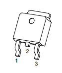


 工商网监
湘ICP备2023018690号
工商网监
湘ICP备2023018690号

