JIANGSU CHANGJING ELECTRONICS TECHNOLOGY CO., LTD
45V Low Current Consumption 250mA CMOS Voltage Regulator
CJ86 XX Series
INTRODUCTION
The CJ86XX series are a group of
positive voltage regulators manufactured
by CMOS technologies with low power
consumption and low dropout voltage,
which provide large output currents even
when the difference of the input-output
voltage is small.
The CJ86XX series can deliver 250mA
output current and allow an input voltage
as high as 45V. The series are very
suitable for the battery-powered
equipments, such as RF applications and
other systems requiring a quiet voltage
source.
Wireless Communication Equipments
Portable Audio Video Equipments
Car Navigation Systems
FEATURES
Low Quiescent Current: 2μA
Operating Voltage Range: 2.5V~45V
Output Current: 250mA
Low Dropout Voltage:
700mV@100mA(VOUT=3.3V)
Output Voltage: 2.1~ 12V
High Accuracy: ±2%/±1%(Typ.)
High Power Supply Rejection Ratio:
70dB@1kHz
Low Output Noise:
27xVOUT μVRMS(10Hz~100kHz)
Excellent Line and Load Transient Response
APPLICATIONS
Cordless Phones
Radio control systems
Laptop, Palmtops and PDAs
Single-lens reflex DSC
Built-in Current Limiter, Short-Circuit
Protection
Over-Temperature Protection
PC peripherals with memory
Stable with Ceramic or Tantalum Capacitor
LAN Cards
Ultra Low Power Microcontrollers
PACKAGING INFORMATION
BLOCK DIAGRAM
SOT-89-3L
Short Circuit Current
Fold-back
+
VIN
Current
Limiter
Thermal Protection
Voltage
Reference
www.jscj-elec.com
R2
VOUT
1.GND
R1
2.IN
VSS
3.OUT
1
Rev. - 1..1
�Electrical Characteristics
ABSOLUTE MAXIMUM RATINGS(1)
(Unless otherwise specified, TA=25°C)
SYMBOL
RATINGS
UNITS
VIN
-0.3~50
V
VOUT
-0.3~12
V
IOUT
250
mA
SOT-89-3L
PD
0.6
W
Range(3)
Tj
-40~+125
°C
TA
-40~+85
°C
Tstg
-40~+125
°C
Tsolder
260°C, 10s
PARAMETER
Input
Voltage(2)
Output Voltage
(2)
Output Current
Power Dissipation
Operating Junction Temperature
Operating Ambient Temperature
Storage Temperature
Soldering Temperature
(1) Stresses beyond those listed under absolute maximum ratings may cause permanent damage to the device.
These are stress ratings only, and functional operation of the device at these or any other conditions beyond
those indicated under recommended operating conditions is not implied. Exposure to absolute-maximum-rated
conditions for extended periods my affect device reliability.
(2) All voltages are with respect to network ground terminal.
(3) This IC includes over temperature protection that is intended to protect the device during momentary overload. Junction temperature will exceed 125°C when over temperature protection is active. Continuous operation
above the specified maximum operating junction temperature may impair device reliability.
RECOMMENDED OPERATING CONDITIONS
PARAMETER
MIN.
NOM.
MAX.
UNITS
Supply voltage at VIN
2.5
45
V
Operating junction temperature range, Tj
-40
125
°C
Operating free air temperature range, TA
-40
85
°C
MODEL DEFINITION INFORMATION
www.jscj-elec.com
Model
Output Voltage
CJ8633
3.3V
CJ8636
3.6V
CJ8650
5.0V
CJ86120
12V
3
Rev. - 1.1
�Electrical Characteristics
CJ86XX Series (VIN=VOUT+2V, CIN=COUT=1μF,TA=25℃, unless otherwise specified)
MAX.
PARAMETER
SYMBOL
CONDITIONS
MIN.
TYP.(4)
UNITS
Input Voltage
VIN
2.5
-
45
V
Output Voltage Range
VOUT
2.1
-
12
V
-2
-
2
%
-1
-
1
%
DC Output Accuracy
IOUT=10mA
Dropout Voltage
Vdif(5)
IOUT =100mA,VOUT=3.3V
-
700
-
mV
Supply Current
ISS
∆VOUT
VOUT × ∆VIN
IOUT=0A
-
2
10
μA
IOUT =10mA
VOUT +1V≤VIN≤36V
-
0.01
0.3
%/V
VIN= VOUT +2V,
1mA≤IOUT≤100mA
-
8
-
mV
Line Regulation
Load Regulation
Temperature
Coefficient
Output Current Limit
Short Current
∆VOUT
∆VOUT
VOUT × ∆TA
ILIM
IOUT=40mA,
-40°C
很抱歉,暂时无法提供与“CJ8633”相匹配的价格&库存,您可以联系我们找货
免费人工找货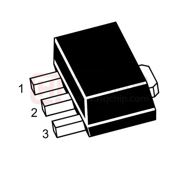


 工商网监
湘ICP备2023018690号
工商网监
湘ICP备2023018690号
