JIANGSU CHANGJING ELECTRONICS TECHNOLOGY CO., LTD
Digital Transistors (Built-in Resistors)
DTA143ZM/DTA143ZE/DTA143ZUA
DTA143ZKA /DTA143ZCA/DTA143ZSA
·Equivalent Circuit
DIGITAL TRANSISTOR (PNP)
FEATURES
Built-in bias resistors enable the configuration of an inverter circuit
without connecting external input resistors(see equivalent circuit)
The bias resistors consist of thin-film resistors with complete isolation to
allow positive biasing of the input.They also have the advantage of
almost completely eliminating parasitic effects
Only the on/off conditions need to be set for operation, making device design easy
PIN CONNENCTIONS and MARKING
DTA143ZM
SOT-723
3
DTA143ZE
SOT-523
3
1. IN
1. IN
2. GND
1
2. GND
1
3. OUT
2
DTA143ZUA
3
DTA143ZKA
SOT-323
3
1. IN
2. GND
1
3. OUT
3
1
www.jscj-elec.com
3. OUT
2
2
DTA143ZCA
SOT-23-3L
1. IN
2. GND
1
3. OUT
2
SOT-23
DTA143ZSA
TO-92S
1. IN
1. GND
2. GND
2. OUT
3. OUT
3. IN
2
1 2 3
1
Rev. - 2.1
�ORDERING INFORMATION
Part Number
MARKING
(1)
Package
Packing Method
Pack Quantity
DTA143=M
E13
SOT-723
Reel
8000pcs/Reel
DTA143=E
E13
SOT-523
Reel
3000pcs/Reel
DTA143=UA
113
SOT-323
Reel
3000pcs/Reel
DTA143=KA
E13
SOT-23-3L
Reel
3000pcs/Reel
DTA143=CA
E13
SOT-23
Reel
3000pcs/Reel
DTA143=SA
A143
Z XXX
(2)
TO-92S
Bulk
1000pcs/Bag
DTA143=SA-TA
A143
Z XXX
(2)
TO-92S
Tape
3000pcs/Box
z
z
z
z
(1). Solid dot = Green molding compound device, if none, the normal device.
Notes:
(2). ;;; &RGH �
MAXIMUM RATINGS(Ta=25℃ unless otherwise noted)
Symbol
Limits(DTA143Z□)
Parameter
M
E
UA
KA
CA
SA
Unit
VCC
Supply Voltage
VIN
Input Voltage
IO
Output Current
PD
Power Dissipation
Tj
Junction Temperature
150
℃
Tstg
Storage Temperature
-55~+150
℃
100
150
-50
V
-30~+5
V
-100
mA
200
200
200
300
mW
ELECTRICAL CHARACTERISTICS (Ta=25℃ unless otherwise specified)
Parameter
Input voltage
Output voltage
Input current
Symbol
Conditions
Min
Typ
Max
VI(off)
VCC=-5V,IO=-100µA
VI(on)
VO=-0.3V,IO=-5mA
-1.3
V
VO(on)
IO/II=-5mA/-0.25mA
-0.3
V
VI=-5V
-1.8
mA
VCC=-50V,VI=0
-0.5
μA
kΩ
II
-0.5
V
Output current
IO(off)
DC current gain
GI
Input resistance
R1
3.29
4.7
6.11
Resistance ratio
R2/R1
8
10
12
Transition frequency
www.jscj-elec.com
Unit
fT
VO=-5V,IO=-10mA
VO=-10V,IO=-5mA,f=100MHz
2
80
250
MHz
Rev. - 2.1
�Typical Characteristics
ON Characteristics
-100
OFF Characteristics
-10
VCC=-5V
VO=-0.3V
-3
(mA)
(V)
-30
Ta=100 ℃
-1
OUTPUT CURRENT
INPUT VOLTAGE
IO
VI(ON)
-10
-3
Ta=25℃
-1
Ta=100℃
-0.3
Ta=25℃
-0.1
-0.03
-0.3
-0.1
-0.1
-1
-0.3
-10
-3
OUTPUT CURRENT
GI
1000
——
IO
-30
-0.01
-0.2
-100
-0.4
(mA)
-0.6
-0.8
INPUT VOLTAGE
VI(OFF)
VO(ON) ——
IO
-1.0
IO
-1000
VO=-5V
-1.2
(V)
IO/II=20
(mV)
300
-300
V0
Ta=25℃
OUTPUT VOLTAGE
DC CURRENT GAIN
GI
Ta=100℃
100
30
10
-100
Ta=100℃
Ta=25℃
-30
3
1
-0.1
-1
-0.3
-10
-3
OUTPUT CURRENT
CO
——
IO
-30
-10
-0.1
-100
-0.3
-3
-1
OUTPUT CURRENT
(mA)
PD
VR
12
——
-10
IO
-30
-100
125
150
(mA)
Ta
400
f=1MHz
Ta=25℃
350
PD
8
POWER DISSIPATION
OUTPUT CAPACITANCE
CO
(pF)
(mW)
10
6
4
300
DTA143ZSA
250
200
DTA143ZUA/CA/KA
DTA143ZE
150
100
DTA143ZM
2
50
0
-0
-4
-8
-12
REVERSE BIAS VOLTAGE
www.jscj-elec.com
-16
VR
0
-20
(V)
0
25
50
75
AMBIENT TEMPERATURE
3
100
Ta
(℃ )
Rev. - 2.1
�SOT-723 Package Outline Dimensions
Dimensions In Millimeters
Min.
Max.
0.430
0.500
0.000
0.050
0.170
0.270
0.270
0.370
0.080
0.150
1.150
1.250
1.150
1.250
0.750
0.850
0.800TYP.
7° REF.
Symbol
A
A1
b
b1
c
D
E
E1
e
θ
Dimensions In Inches
Min.
Max.
0.017
0.020
0.000
0.002
0.007
0.011
0.011
0.015
0.003
0.006
0.045
0.049
0.045
0.049
0.030
0.033
0.031TYP.
7° REF.
SOT-723 Suggested Pad Layout
NOTICE
JSCJ reserves the right to make modifications,enhancements,improvements,corrections or other
changes without further notice to any product herein. JSCJ does not assume any liability arising
out of the application or use of any product described herein.
www.jscj-elec.com
4
Rev. - 2.1
�SOT-723 Tape and Reel
www.jscj-elec.com
5
Rev. - 2.1
�SOT-523 Package Outline Dimensions
Symbol
A
A1
A2
b1
b2
c
D
E
E1
e
e1
L
L1
θ
Dimensions In Millimeters
Min.
Max.
0.700
0.900
0.000
0.100
0.700
0.800
0.150
0.250
0.250
0.350
0.100
0.200
1.500
1.700
0.700
0.900
1.450
1.750
0.500 TYP.
0.900
1.100
0.400 REF.
0.260
0.460
0°
8°
Dimensions In Inches
Max.
Min.
0.028
0.035
0.000
0.004
0.028
0.031
0.006
0.010
0.010
0.014
0.004
0.008
0.059
0.067
0.028
0.035
0.057
0.069
0.020 TYP.
0.035
0.043
0.016 REF.
0.010
0.018
0°
8°
SOT-523 Suggested Pad Layout
NOTICE
JSCJ reserves the right to make modifications,enhancements,improvements,corrections or other
changes without further notice to any product herein. JSCJ does not assume any liability arising
out of the application or use of any product described herein.
www.jscj-elec.com
6
Rev. - 2.1
�SOT-523 Tape and Reel
www.jscj-elec.com
7
Rev. - 2.1
�SOT-323 Package Outline Dimensions
Dimensions In Millimeters
Min
Max
0.900
1.100
0.000
0.100
0.900
1.000
0.200
0.400
0.080
0.150
2.000
2.200
1.150
1.350
2.150
2.450
0.650 TYP
1.200
1.400
0.525 REF
0.260
0.460
0°
8°
Symbol
A
A1
A2
b
c
D
E
E1
e
e1
L
L1
θ
Dimensions In Inches
Min
Max
0.035
0.043
0.000
0.004
0.035
0.039
0.008
0.016
0.003
0.006
0.079
0.087
0.045
0.053
0.085
0.096
0.026 TYP
0.047
0.055
0.021 REF
0.010
0.018
0°
8°
SOT-323 Suggested Pad Layout
NOTICE
JSCJ reserves the right to make modifications,enhancements,improvements,corrections or other
changes without further notice to any product herein. JSCJ does not assume any liability arising
out of the application or use of any product described herein.
www.jscj-elec.com
8
Rev. - 2.1
�SOT-323 Tape and Reel
www.jscj-elec.com
9
Rev. - 2.1
�������-3L�
��
���������������������
Symbol
A
A1
A2
b
c
D
E1
E
e
e1
L
�
Dimensions In Millimeters
Min.
Max.
1.050
1.250
0.000
0.100
1.050
1.150
0.300
0.500
0.100
0.200
2.820
3.020
1.500
1.700
2.650
2.950
0.950(BSC)
1.800
2.000
0.300
0.600
0°
8°
Dimensions In Inches
Max.
Min.
0.041
0.049
0.000
0.004
0.041
0.045
0.012
0.020
0.004
0.008
0.111
0.119
0.059
0.067
0.104
0.116
0.037(BSC)
0.071
0.079
0.012
0.024
0°
8°
������-3L���
������
���
�����
NOTICE
JSCJ reserves the right to make modifications,enhancements,improvements,corrections or other
changes without further notice to any product herein. JSCJ does not assume any liability arising
out of the application or use of any product described herein.
www.jscj-elec.com
10
Rev. - 2.1
�SOT-23-3L Tape and Reel
www.jscj-elec.com
11
Rev. - 2.1
�SOT-23 Package Outline Dimensions
Symbol
A
A1
A2
b
c
D
E
E1
e
e1
L
L1
θ
Dimensions In Millimeters
Min
Max
0.900
1.150
0.000
0.100
0.900
1.050
0.300
0.500
0.080
0.150
2.800
3.000
1.200
1.400
2.250
2.550
0.950 TYP
1.800
2.000
0.550 REF
0.300
0.500
0°
8°
Dimensions In Inches
Min
Max
0.035
0.045
0.000
0.004
0.035
0.041
0.012
0.020
0.003
0.006
0.110
0.118
0.047
0.055
0.089
0.100
0.037 TYP
0.071
0.079
0.022 REF
0.012
0.020
0°
8°
SOT-23 Suggested Pad Layout
NOTICE
JSCJ reserves the right to make modifications,enhancements,improvements,corrections or other
changes without further notice to any product herein. JSCJ does not assume any liability arising
out of the application or use of any product described herein.
www.jscj-elec.com
12
Rev. - 2.1
�SOT-23 Tape and Reel
www.jscj-elec.com
13
Rev. - 2.1
�Dimensions In Millimeters
Min.
Max.
1.420
1.620
0.660
0.860
0.330
0.480
0.400
0.510
0.330
0.510
3.900
4.100
2.280
2.680
3.050
3.250
1.270 TYP.
2.440
2.640
15.100
15.500
45° TYP.
Symbol
A
A1
b
b1
c
D
D1
E
e
e1
L
θ
Dimensions In Inches
Min.
Max.
0.056
0.064
0.026
0.034
0.013
0.019
0.016
0.020
0.013
0.020
0.154
0.161
0.090
0.106
0.120
0.128
0.050 TYP.
0.096
0.104
0.594
0.610
45° TYP.
NOTICE
JSCJ reserves the right to make modifications,enhancements,improvements,corrections or other
changes without further notice to any product herein. JSCJ does not assume any liability arising
out of the application or use of any product described herein.
www.jscj-elec.com
14
Rev. - 2.1
�www.jscj-elec.com
15
Rev. - 2.1
�
很抱歉,暂时无法提供与“DTA143ZUA”相匹配的价格&库存,您可以联系我们找货
免费人工找货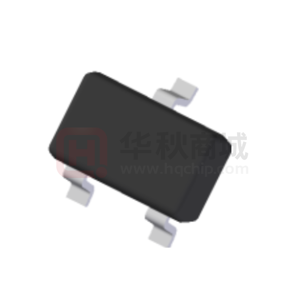


 工商网监
湘ICP备2023018690号
工商网监
湘ICP备2023018690号
