JMTL3400A
Description
JMT N-channel Enhancement Mode Power MOSFET
Features
Application
30V,5.8A
RDS(ON)< 26mΩ @ VGS =10V
RDS(ON)< 32mΩ @ VGS =4.5V
RDS(ON)< 50mΩ @ VGS =2.5V
Load Switch
PWM Application
Power management
Advanced Trench Technology
Excellent RDS(ON) and Low Gate Charge
Lead free product is acquired
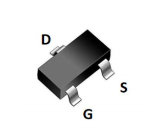
SOT-23 top view
Marking and pin Assignment
Schematic Diagram
Package Marking and Ordering Information
Device Marking
Device
OUTLINE
Device Package
Reel Size
Reel
(PCS)
Per Carton
(PCS)
3400
JMTL3400A
TAPING
SOT-23
7inch
3000
180000
Absolute Maximum Ratings (TA=25℃ unless otherwise specified)
Symbol
Parameter
Max.
Units
VDSS
Drain-Source Voltage
30
V
VGSS
Gate-Source Voltage
±12
V
TA = 25℃
5.8
A
TA = 100℃
3.8
A
23.2
A
1.36
W
92
℃/W
-55 to +150
℃
ID
Continuous Drain Current
IDM
Pulsed Drain Current note1
PD
Power Dissipation
RθJA
TJ, TSTG
TA = 25℃
Thermal Resistance, Junction to Ambient
Operating and Storage Temperature Range
JieJie Microelectronics CO. , Ltd
Version :1.3
- 1 -
�JMTL3400A
Electrical Characteristics (TJ=25℃ unless otherwise specified)
Symbol
Parameter
Test Condition
Min.
Typ.
Max.
Units
Off Characteristic
V(BR)DSS
Drain-Source Breakdown Voltage
VGS=0V, ID=250μA
30
-
-
V
IDSS
Zero Gate Voltage Drain Current
VDS=30V, VGS=0V,
-
-
1.0
μA
IGSS
Gate to Body Leakage Current
VDS=0V, VGS= ±12V
-
-
±100
nA
VDS=VGS, ID=250μA
0.5
0.9
1.4
V
VGS=10V, ID=4.2A
-
19
26
VGS=4.5V, ID=4A
-
23
32
VGS=2.5V, ID=1A
-
35
50
-
702
-
pF
-
66
-
pF
-
52
-
pF
-
4.8
-
nC
-
1.2
-
nC
-
1.7
-
nC
-
12
-
ns
-
52
-
ns
-
17
-
ns
-
10
-
ns
On Characteristics
VGS(th)
RDS(on)
Gate Threshold Voltage
Static Drain-Source on-Resistance
note2
mΩ
Dynamic Characteristics
Ciss
Input Capacitance
Coss
Output Capacitance
Crss
Reverse Transfer Capacitance
Qg
Total Gate Charge
Qgs
Gate-Source Charge
Qgd
Gate-Drain(“Miller”) Charge
VDS=15V, VGS=0V,
f=1.0MHz
VDS=15V, ID=4A,
VGS=4.5V
Switching Characteristics
td(on)
Turn-on Delay Time
tr
Turn-on Rise Time
td(off)
Turn-off Delay Time
tf
Turn-off Fall Time
VDS=15V,
ID=4A, RGEN=3Ω,
VGS=4.5V
Drain-Source Diode Characteristics and Maximum Ratings
IS
Maximum Continuous Drain to Source Diode Forward
Current
-
-
5.8
A
ISM
Maximum Pulsed Drain to Source Diode Forward Current
-
-
23.2
A
VSD
Drain to Source Diode Forward
Voltage
-
-
1.2
V
VGS=0V, IS=5.8A
Notes:1. Repetitive Rating: Pulse Width Limited by Maximum Junction Temperature
2. Pulse Test: Pulse Width≤300μs, Duty Cycle≤0.5%
JieJie Microelectronics CO. , Ltd
Version :1.3
- 2 -
�JMTL3400A
Typical Performance Characteristics
Figure 2: Typical Transfer Characteristics
Figure1: Output Characteristics
25
ID (A)
10V
20
ID (A)
25
4.5V
V DS=5V
20
3V
2.5V
15
15
125℃
10
10
2V
25℃
5
5
V DS(V)
0
0
1
2
3
4
0
5
0.5
1.0
1.5
2.0
2.5
3.0
Figure 4: Body Diode Characteristics
Figure 3:On-resistance vs. Drain Current
IS(A)
RDS(ON) (mΩ)
60
VGS(V)
0
103
50
40
102
TJ=125℃
V GS=2.5V
30
V GS=4.5V
TJ=25℃
101
20
VGS=10V
10
0
VGS=0V
ID(A)
0
1
2
3
4
100
0.2
5
Figure 5: Gate Charge Characteristics
5
4
0.4
0.6
V SD(V)
1.0
1.2
1.4
1.6
1.8
Figure 6: Capacitance Characteristics
VGS(V)
104
VDS=15V
ID=4A
3
2
C(pF)
103
Ciss
102
Coss
1
0
0
0.8
C rss
Q g(nC)
1
2
3
4
101
5
JieJie Microelectronics CO. , Ltd
V DS(V)
0
5
10
15
20
25
Version :1.3
- 3 -
�JMTL3400A
Figure 7: Normalized Breakdown Voltage vs.
Junction Temperature
Figure 8: Normalized on Resistance vs.
Junction Temperature
V BR(DSS)
1.3
2.5
1.2
RDS (on)
2.0
1.1
1.5
1.0
1.0
0.9
Tj (℃ )
0
-100
-50
0
50
100
150
0.5
-100
200
Figure 9: Maximum Safe Operating Area
6
100
10
100μs
0.01
0.01
ID(A)
1
DC
VDS (V)
1
200
2
10ms
0.1
150
3
1ms
T A=25℃
Single pulse
100
4
10μs
0.1
50
5
1μs
Limited by R DS(on)
0
Figure 10: Maximum Continuous Drain Current
vs. Ambient Temperature
ID(A)
1
Tj (℃ )
-50
10
0
100
0
25
50
T A (℃ )
75
100
125
150
175
Figure.11: Maximum Effective Transient Thermal
Impedance, Junction-to-Ambient
103
ZthJ-A(℃ /W)
100
D=0.5
D=0.2
D=0.1
D=0.05
D=0.02
D=0.01
Single pulse
10-1
10-2 -6
10
10-5
10-4
10-3
TP (s)
10-2
PDM
102
t1
t2
Notes:
1.Duty factor D=t1/t2
2.Peak T J=P DM *Z thJA +T A
10-1
100
101
JieJie Microelectronics CO. , Ltd
Version :1.3
- 4 -
�JMTL3400A
Test Circuit
Figure1:Gate Charge Test Circuit & Waveform
Figure 2: Resistive Switching Test Circuit & Waveforms
Figure 3:Unclamped Inductive Switching Test Circuit & Waveforms
JieJie Microelectronics CO. , Ltd
Version :1.3
- 5 -
�JMTL3400A
Package Mechanical Data-SOT-23
Dimensions
Ref.
Millimeters
Min.
Typ.
Max.
A
2.30
2.40
2.50
0.091 0.095 0.098
I
B
2.80
2.90
3.00
0.110 0.114 0.118
E
A
B
F
SOT-23
Typ.
Max.
0.075 REF
D
0.35
0.40
0.45
0.014 0.016 0.018
E
1.20
1.30
1.40
0.047 0.051 0.055
F
0.90
1.00
1.10
0.035 0.039 0.043
0.10
0.15
0.004 0.006
G
D
Min.
1.90 REF
C
C
Inches
H
G
H
0.20
I
0
0.008
0.10
0
0.004
P0
P2
D0
Package Information-SOT-23
A0
W
B0
F
E
Ref.
P1
JieJie Microelectronics CO. , Ltd
Dimensions
Millimeters
Inches
A0
3.15 ± 0.3
0.124 ± 0.012
B0
2.77 ± 0.3
0.109 ± 0.012
C
178
7.0
D0
1.50±0.1
0.059 ± 0.004
E
1.75 ± 0.2
0.069 ± 0.008
E1
13.3±0.3
0.524± 0.012
F
3.5 ± 0.2
0.138 ± 0.008
P0
4.00 ± 0.2
0.157 ± 0.008
P1
4.00 ± 0.2
0.157 ± 0.008
P2
2.00 ± 0.2
0.079 ± 0.008
W
8.00 ± 0.2
0.315 ± 0.008
W1
11.5±1.0
0.453 ± 0.039
Version :1.3
- 6 -
�JMTL3400A
Information furnished in this document is believed to be accurate and reliable. However, Jiangsu
JieJie Microelectronics Co.,Ltd assumes no responsibility for the consequences of use without
consideration for such information nor use beyond it.
Information mentioned in this document is subject to change without notice, apart from that
when an agreement is signed, Jiangsu JieJie complies with the agreement.
Products and information provided in this document have no infringement of patents. Jiangsu
JieJie assumes no responsibility for any infringement of other rights of third parties which may
result from the use of such products and information.
is a registered trademark of Jiangsu JieJie Microelectronics Co.,Ltd.
Copyright ©2020Jiangsu JieJie Microelectronics Co.,Ltd. Printed All rights reserved.
JieJie Microelectronics CO. , Ltd
Version :1.3
- 7 -
�
很抱歉,暂时无法提供与“JMTL3400A”相匹配的价格&库存,您可以联系我们找货
免费人工找货- 国内价格
- 1+0.20925
- 10+0.20150
- 100+0.18290
- 500+0.17360


 工商网监
湘ICP备2023018690号
工商网监
湘ICP备2023018690号


