High Frequency Ceramic Solutions
P/N 2450AT42E0100
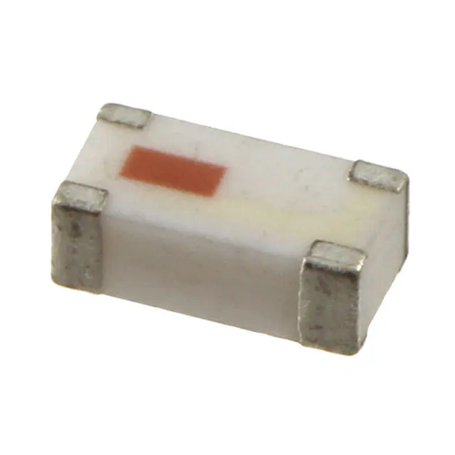
2.4 GHz SMD, Above Metal, Low Profile Mini Chip Antenna
This antenna will generally have a metal layer directly underneath for proper operation, exceptions may apply.
Detail Specification:
Page 1 of 8
10/28/2021
General Specifications
Part Number
Frequency (MHz)
Peak Gain (dBi typ.)
Average Gain (dBi typ.)
Return Loss (dB)
Impedance (Ω)
Power Capacity (W)
Reel Quantity (pcs./reel)
Operating Temp
2450AT42E0100
2400 - 2480
-2.0 (YZ-V)
-5.0 (YZ-V)
5.6 typ. (4.5 min.)
50
2 max. (CW)
2,000
-40 to +85°C
+5°C to +35°C
Humidity 45 - 75% RH
18 months max.
Recommended Storage
Conditions and Period for
unused Product on T&R
Antenna mounts
directly above or
below the metal layer
of PCB. No antenna
clearance required
ever again!
Total average radiated efficiency on PCB feature on "Mounting Considerations 1" ( orderable EVB p/n: 2450AT42E0100-EB1SMA) is ~30%
This antenna was designed in mind for small coin cell, wearable, IoT, 2.4 BLE, 802.11, ISM, Zigbee, etc. applications in
close-range networks where metal or a battery/display covers the entire length or side of the PCB or encasement must be
present directly under the antenna and there's no room for usual/typical antenna metal clearance.
This antenna is specifically designed for PCBs that have 0.5-1mm of total thickness
Part Number Explanation
P/N Suffix
Suffix = S
E.g. 2450AT42E0100S
Bulk (loose pcs.)
T&R
Suffix = E
E.g. 2450AT42E0100E
2450AT42E0100-EB1SMA (comes with 1 female SMA connector)
Packing Style
Evaluation Board
Mechanical Specifications
L
W
T
a
b
C
0.197
0.079
0.059
0.020
0.059
0.012
In
± 0.008
± 0.008
± 0.008
± 0.008
± 0.008
max
Terminal Configuration
mm
5.00 ± 0.20
2.00 ± 0.20
1.50 ± 0.20
0.50 ± 0.20
1.50 ± 0.20
0.30 max
W
c
L
Top View
b
T
b
a
NC1
GND
GND
1
Bottom View
Side View
Feeding Point
1
2
3
4
Make sure to have Pin 2 soldered
to its PCB land pad but not
connected to GND or input, it must
be NC (or floating).
Johanson Technology, Inc. reserves the right to make design changes without notice.
All sales are subject to Johanson Technology, Inc. terms and conditions.
https://www.johansontechnology.com
4001 Calle Tecate • Camarillo, CA 93012 • TEL 805.389.1166 FAX 805.389.1821
Ver. 4.0
2021 Johanson Technology, Inc. All Rights Reserved
�High Frequency Ceramic Solutions
P/N 2450AT42E0100
2.4 GHz SMD, Above Metal, Low Profile Mini Chip Antenna
This antenna will generally have a metal layer directly underneath for proper operation, exceptions may apply.
Page 2 of 8
10/28/2021
Detail Specification:
Mounting Considerations 1
Top View
Bottom View
3mm
Ground
6.26mm
Matching circuit
30mm
50Ω Feed Line
Ground Plane (where other SMD
components will be mounted)
p/n: 2450AT42E0100-EB1SMA
50mm
Want the layout file? Send us a message at:
https://www.johansontechnology.com/ask-a-question
Metal bottom GND plane to be placed directly
underneath yellow soldemask zone, covering
entire area.
0.63mm 1.5mm
2mm
1.5mm
0.63mm
0.3mm
3.3 nH
1.0mm
2.0 pF
*
0.6mm
1.5 nH
3mm
0.6mm
0.5mm
6.26mm
Floating pad
Matching circuit
*Line width should be designed to match 50ohm characteristic impedance, depending on PCB material and
thickness. A coplanar waveguide trace is recommended for best results.
For this particular antenna It is recommended that the designer leave available slots for the matching network, even
if all slots won't be used, this will prepare the PCB for the unpredictable final mass production version of the
matching circuit. The antenna matching network values above are used when antenna is mounted on Johanson's
evaluation board. The matching values on client’s PCB will be different.
To order a pre-tuned 50Ω EVB with a female SMA connector you see here Click here:
https://www.johansontechnology.com/request-a-sample
Reference p/n: 2450AT42E0100-EB1SMA
Johanson Technology, Inc. reserves the right to make design changes without notice.
All sales are subject to Johanson Technology, Inc. terms and conditions.
https://www.johansontechnology.com
4001 Calle Tecate • Camarillo, CA 93012 • TEL 805.389.1166 FAX 805.389.1821
Ver. 4.0
2021 Johanson Technology, Inc. All Rights Reserved
�High Frequency Ceramic Solutions
P/N 2450AT42E0100
2.4 GHz SMD, Above Metal, Low Profile Mini Chip Antenna
This antenna will generally have a metal layer directly underneath for proper operation, exceptions may apply.
Page 3 of 8
10/28/2021
Detail Specification:
Typical Electrical Characteristics (T=25 °C)
Return Loss
0
m122
m123
dB(S(1,1))
-5
-10
m118
-15
-20
2.0
2.2
2.4
2.6
2.8
3.0
freq, GHz
m122
m123
m118
freq=2.400GHz
freq=2.480GHz
freq=2.440GHz
dB(S(1,1))=-5.691 dB(S(1,1))=-11.343 dB(S(1,1))=-5.746
The designer should not be highly concerned of the fact that the antenna only demonstrates a -5dB
S11 level at the band edges. The antenna has sufficient gain at the band edges to satisfy the
applications and uses a high dielectric constant ceramic giving it some detuning resilience to
capacitivel loading effects. This antenna is designed for close proximity applications such as the
ones mentioned on page 1.
Johanson Technology, Inc. reserves the right to make design changes without notice.
All sales are subject to Johanson Technology, Inc. terms and conditions.
https://www.johansontechnology.com
4001 Calle Tecate • Camarillo, CA 93012 • TEL 805.389.1166 FAX 805.389.1821
Ver. 4.0
2021 Johanson Technology, Inc. All Rights Reserved
�High Frequency Ceramic Solutions
2.4 GHz SMD, Above Metal, Low Profile Mini Chip Antenna
P/N 2450AT42E0100
This antenna will generally have a metal layer directly underneath for proper operation, exceptions may apply.
Detail Specification:
Page 4 of 8
10/28/2021
Typical Radiation Patterns @ 2.44GHz (T=25 °C)
Y :Φ(Phi)=90°
XY-plane @2440MHz
Total
X :Φ(Phi)=0°
Z : θ(Theta)=0°
XZ-plane @2440MHz
Total
YZ-plane @2440MHz
Total
Johanson Technology, Inc. reserves the right to make design changes without notice.
All sales are subject to Johanson Technology, Inc. terms and conditions.
https://www.johansontechnology.com
4001 Calle Tecate • Camarillo, CA 93012 • TEL 805.389.1166 FAX 805.389.1821
Ver. 4.0
2021 Johanson Technology, Inc. All Rights Reserved
�High Frequency Ceramic Solutions
P/N 2450AT42E0100
2.4 GHz SMD, Above Metal, Low Profile Mini Chip Antenna
This antenna will generally have a metal layer directly underneath for proper operation, exceptions may apply.
Detail Specification:
Page 5 of 8
10/28/2021
Mounting Considerations 2 - Circular PCB Environments (coin cell type)
Top View
0.63mm 1.5mm
2mm
1.5mm 0.63mm
0.3mm
0.6mm
1.0mm
Matching circuit
0.6mm
0.5mm
50Ω Feed Line
radius=22mm
(reference only)
Ground
Receding the GND plane may sound counterintuitive, but this helps shape the radiation pattern in
a more isometric (spherical) shape. We recommend
the designer do this of he/she can afford the reduce
SMT space, but not mandated.
)
31.7mm
7mm
Bottom View
0.3mm
6.26mm
radius=22mm
Ground
Want the layout file? Send us a message at:
https://www.johansontechnology.com/ask-a-question
31.7mm
7mm
Note: There's no orderable EVB available for the above "Mounting Considerations 2" reference design
Johanson Technology, Inc. reserves the right to make design changes without notice.
All sales are subject to Johanson Technology, Inc. terms and conditions.
https://www.johansontechnology.com
4001 Calle Tecate • Camarillo, CA 93012 • TEL 805.389.1166 FAX 805.389.1821
Ver. 4.0
2021 Johanson Technology, Inc. All Rights Reserved
�High Frequency Ceramic Solutions
P/N 2450AT42E0100
2.4 GHz SMD, Above Metal, Low Profile Mini Chip Antenna
This antenna will generally have a metal layer directly underneath for proper operation, exceptions may apply.
Detail Specification:
Page 6 of 8
10/28/2021
Mounting Considerations 3 - Recommendations when using 2450AT42E010B
We have found that the best performance can be gained when using the 2450AT42E010B with a 4layer PCB with a total thickness approximately 1.5mm thick.
50mm
3mm
Ground
6.26mm
Matching circuit
30mm
50Ω Feed Line
2450AT42E010B evaluation board (PN 2450AT42E010B-EB1SMA)
Want the layout file? Send us a message at:
https://www.johansontechnology.com/ask-a-question
The 2450AT42E010B 4-layer evaluation board has the following stackup:
6 mil
41 mil
To order a pre-tuned 50Ω EVB with a female
SMA connector, click here:
https://www.johansontechnology.com/request-a-sample
Reference p/n: 2450AT42E010B-EB1SMA
6 mil
Johanson Technology, Inc. reserves the right to make design changes without notice.
All sales are subject to Johanson Technology, Inc. terms and conditions.
https://www.johansontechnology.com
4001 Calle Tecate • Camarillo, CA 93012 • TEL 805.389.1166 FAX 805.389.1821
Ver. 4.0
2021 Johanson Technology, Inc. All Rights Reserved
�High Frequency Ceramic Solutions
P/N 2450AT42E0100
2.4 GHz SMD, Above Metal, Low Profile Mini Chip Antenna
This antenna will generally have a metal layer directly underneath for proper operation, exceptions may apply.
Detail Specification:
Page 7 of 8
10/28/2021
How To Choose The Correct Antenna Variant
Since the antenna's efficiency is largely affected by the thickness of the PCB's substrate, we offer another variant of
this antenna. This allows a more robist design to fit your PCB. The disparity between antenna variations are internal
only; variations are identical in dimension and footprint-compatible.
Refer to the diagram below to understand what is meant by substrate thickness.
*Substrate Thickness (H)
*For PCBs consisting of multiple layers, the thickness (H) is limited distance between the metal layer immediately below the antenna.
PCB Substrate Thickness
Recommended JTI PN
≤ 1.0mm
2450AT42E0100
1.0mm - 2.0mm
2450AT42E010B
Typical Efficiency Values @ 2.44GHz for various scenarios for a 30x50mm PCB
The following efficiency values represent performance on a 30x50mm EVB like on page 2. Please note that antenna
efficiency varies widely with board layout, size and surroundings.
PCB
Substrate
Thickness
(H)
Antenna Efficiency @ 2.44GHz
2450AT42E0100
2450AT42E010B
H = 0.12 mm
1.95%
1.02%
H = 0.7 mm
29.20%
9.30%
H = 1.5 mm
23.30%
38.00%
H = 2.5 mm
21.60%
42.00%
Note: "H" substrate thickness of


 工商网监
湘ICP备2023018690号
工商网监
湘ICP备2023018690号
