ECP5™ PCI Express Board
User’s Guide
July 2014
EB91_1.0
�ECP5 PCI Express Board User’s Guide
Introduction
The ECP5™ PCI Express Board allows designers to investigate and experiment with the features of the ECP5
Field-Programmable Gate Array. The features of the ECP5 PCI Express Board can assist engineers with rapid prototyping and testing of their specific designs. The guide is intended to be referenced in conjunction with demo
user’s guides to demonstrate the ECP5 FPGA.
Figure 1. ECP5 PCI Express Board, Top Side
Expansion Connector/Header
Expansion Connector/Header
On-Board Clock
Management
RJ45
Connections
12 V DC Power Input
Configuration Device
Selection Switches
Configuration Switches
LPDDR3
USB Programming
SPI Flash
Configuration
Memory
PMOD Switches
Status LEDs
PCI Express x4
PMOD Connector
User Switches
Features
• PCI Express form-factor
– Allows demonstration of PCI Express x4 interconnection
• USB-B connection for UART and device programming
• One RJ45 interfaces to 10/100/1000 Ethernet to RGMII
• On-board Boot Flash
– 128M Serial SPI Flash
• 8GB LPDDR3 memory components (256Mbx32)
• Expansion connections and headers
– Allows flexibility for user prototype expansion
• Switches, LEDs and displays for demo purposes
• Lattice Diamond® Programmer configuration support
• On-board reference clock sources
• Easy power measurements
– All ECP5 rails have probable power resistors
The contents of this user’s guide include top-level functional descriptions of the various portions of the evaluation
board, descriptions of the on-board connectors, diodes and switches and a complete set of schematics.
2
�ECP5 PCI Express Board User’s Guide
Caution: The ECP5 PCI Express Board contains ESD-sensitive components. ESD safe practices should be followed while handling and using the evaluation board.
ECP5 Device
This board features an ECP5 FPGA in a 756-ball caBGA with a 1.1 V core supply. A complete description of this
device can be found in DS1044, ECP5 Family Data Sheet.
Note: The connections referenced in this document refer to the LFE5UM-85F-7MG756BC device.
Applying Power to the Board
The ECP5 PCI Express Board is ready to power on. The board can be supplied with power from a PCI Express
host system or standalone with an external wall power module.
The 12 V DC input power source is fused with a surface mounted fuse, as noted in Table 1.
Table 1. Board Power Supply Fuses (See Appendix B, "Power Supplies" sheet)
Fuse Designator
Description
F1
12 V Input Supply Fuse
The board may be plugged into a host PC. Only plug the board into a PCI Express slot when the system is powered
off. Once inserted, the PC can be safely powered on.
Using the evaluation board outside of a PC chassis supply requires the factory-supplied wall supply module. Use of
other supplies is not suggested.
Figure 2. Power Distribution Scheme (See Appendix B, "Power Supplies" sheet)
Power Supply Block Diagram
12_0V
(5A Fused)
SW
2_5V, +2.5 V, 1.1 A
SW
3_3V, +3.3 V, 1.35 A
SERDES 1_2V, +1.2 V, 500 mA
LDO
LPDDR3, VDD1 1_2V, +1.2 V, 500 mA
LDO
LDO
SERDES 1_1V, +1.1 V, 500 mA
LPDDR3, VDD1 1_8V, +1.8 V, 100 mA
SW
1_5V, +1.5 V, 1.1 A
SW
VCC_CORE, +1.1 V, 1.35 A
Programming/FPGA Configuration
The ECP5 PCI Express Board has a built-in download controller for programming the ECP5 FPGA. The built-in
module consists of a USB Type-B connector and a USB UART device. To use the built-in down- load cable, simply
connect a standard USB cable (a USB-B to USB-A cable is included with the ECP5 PCI Express Board) from J5 to
3
�ECP5 PCI Express Board User’s Guide
your PC (with Diamond Programmer software installed). The USB hub on the PC will detect the addition of the USB
function, making the built-in cable available for use with the Diamond Programmer software.
Diamond Programmer Requirements
Note: This board includes the built-in download module and only requires the USB cable included with the board.
After initial board setup, use the following procedure to program the board. Instructions assume that Diamond Programmer software has been installed on a local PC.
Requirements:
• PC with Diamond Programmer 3.2 (or later) programming software, installed with appropriate drivers (USB driver
for USB cable).
Note: An option to install these drivers is included as part of the Diamond Programmer setup.
Board Programming
Configuration Status Indicators (See Appendix B, "XO2 Configuration Mux" sheet)
Figure 3. PCI Express Board Configuration/Programming Mux Selection
SW6 is used to select the device to program on the ECP5 PCI Express Board (1=Up, 0=Down).
SW6[1:4]
Device Selected to Program or Configure
1111
MachXO2-640 (JTAG Mux). Note This device must be programmed before Programming or Configuring other devices. This device is pre-programmed during the boards manufacturing.
0000
ECP5UM-85
0001
ispClock-5304 (Clock Management) This device is controls the clock management on the board.
This device is pre-programmed during the boards manufacturing.
0010
Expansion Card on CN1 Connector (Left)
0100
Expansion Card on CN2 Connector (Right)
SW7 includes the ECP5 CFG pins (1=Up, 0=Down) which allow the configuration mode of the ECP5 to be
selected. Switches are the right side of SW7 where SW7[1]=CFG0, SW7[2]=CFG1, SW7[3]=CFG2
4
�ECP5 PCI Express Board User’s Guide
Figure 4. ECP5 Configuration Pin (CFG pins)
Figure 5. ECP5 Status LEDs and Push-button Controls
The LEDs indicate the configuration status of the ECP5 FPGA.
• D10 (red) illuminated indicates that programming was aborted or reinitialized, driving the INITN output low.
• D11 (green) illuminated indicates the successful completion of configuration by releasing the open collector
DONE output pin.
PROGRAMN and GSRN
These push-button switches assert/de-assert the logic levels on PROGRAMN (S2) and GSRN (S1). Depress- ing
the button drives a logic level “0” to the device.
Programming Serial SPI Flash Memory
A serial SPI (16-pin TSSOP, 128Mb) Flash memory device (U52) is on-board for non-volatile configuration memory
storage. A Micron N25Q128A device is populated on-board.
The Serial SPI Flash memory device can be configured easily via the ECP5 JTAG port. This mode enables the
FPGA to be programmed at power-up or assertion of PROGRAMN with a bitstream stored in the memory device.
1. Connect the ECP5 PCI Express Board.
2. Scan the board or select the ECP5UM-85F device.
3. From the Edit pull down menu select Device Properties. Set the Access mode to SPI Flash Background Programming and Operation to SPI Flash Erase, Program, Verify.
5
�ECP5 PCI Express Board User’s Guide
Figure 6. Device Information Dialog Screen
4. Under the SPI Flash Options, select Family to SPI Serial Flash, Vendor to Micron, Device to SPI-N25Q128A,
Package to 16-lead SOIC.
Figure 7. Select Device Dialog Box
5. Click OK in the Device Properties dialog box. You will return to the main configuration screen.
6. Using SW6 set the ECP5 CFG pins to 010.
7. From the main programming window, select Go from the top toolbar. This begins the SPI Serial Flash programming.
6
�ECP5 PCI Express Board User’s Guide
On-Board Clock Capabilities (See Appendix B, "Clock Generation" and "LPDDR3" sheets)
The ECP5 PCI Express Board allows for several clock source options. Some of these options are controlled via the
ispClock5304 programmable clock manager device. The clock manager will be supplied by a 54 MHz clock onboard oscillator or an external clock source. The LPDDR3 clock will be supplied directly from a 100 MHz on board
oscillator.
Table 2. Clock Sources
Clock Destination
ECP5 ball AD32 site
LRC_GPLL0T_IN
ECP5 ball A17 site
ULC_GPLL0T_IN
Clock Sources
Control Switch Setting
54 MHz On board Oscillator X1
SW7[7]=0, ispClock5304 PLL can be used
by setting SW7[8]=1
External Clock J4
SW7[7]=1, ispClock5304 PLL can be used
by setting SW7[8]=1
54 MHz On board Oscillator X1
SW7[7]=0, ispClock5304 PLL can be used
by setting SW7[8]=1
External Clock J4
SW7[7]=1, ispClock5304 PLL can be used
by setting SW7[8]=1
ECP5 ball C5/D5 site ULC
100 MHz On board Oscillator U32
Connector CN1 (Left)
54 MHz On board Oscillator X1
ispClock5304 PLL can be used by setting
SW7[8]=1
Connector CN2 (Right)
54 MHz On board Oscillator X1
ispClock5304 PLL can be used by setting
SW7[8]=1
SERDES
The ECP5 based SERDES FPGA is utilized on the board for several purposes. The SERDES block is provisioned
to provide a single, full-duplex PCI Express channel. The high-speed signals are connected to the PCI Express
edge connection.
7
�ECP5 PCI Express Board User’s Guide
FPGA Test Pins (See Appendix B, "ECP5 Config" and "LEDs and Switches" sheets)
General Purpose DIP Switches
General purpose FPGA pins are available for user applications. FPGA pins are connected to switch SW4, SW7
with a piano style DIP switch. The switches are connected to logic level 0 when Down, logic level 1 when Up.
Switch position 1 is indicated with a dot. Switch SW4 logic 1 is 2.5V. Switch SW4 logic 1 is 2.5V. The user must program these inputs to be the LVCMOS25 or LVCMOS33 type in the design.
Figure 8. ECP5 PCI Express Board LEDs and Switches
The designated pins are connected according to Table 5.
Table 3. FPGA Ball to DIP Switch Position
FPGA Ball Number
SW4 DIP Switch Position
AK31
1
AM31
2
AJ31
3
AL32
4
AG28
5
AJ28
6
AG29
7
AH28
8
FPGA Ball Number
SW7 DIP Switch
Position
F31
4
F32
5
E32
6
8
�ECP5 PCI Express Board User’s Guide
General Purpose LEDs (See Appendix B, "LEDs and Switches" sheet)
The LEDs provided on the ECP5 PCI Express Board are connected to general purpose FPGA I/Os. These LEDs
provide status for user designs and must be included in the design. The LEDs illuminate when the FPGA output is
driven LOW. Table 6 shows the LED and associated FPGA pins. These pins are within an I/O bank connected to
2.5 V and the user should program these to be LVCMOS25 type outputs in the design.
Table 4. LED Definitions
LED Number
FPGA Ball Number
PCB Designator
LED Color
LED1
AM28
D1
Red
LED2
AL28
D2
Red
LED3
AM29
D3
Red
LED4
AK28
D4
Red
LED5
AK32
D5
Red
LED6
AM30
D6
Red
LED7
AJ32
D7
Red
LED8
AL30
D8
Red
LPDDR3 Memory Device (See Appendix B, "LPDDR" sheet)
• The ECP5 PCI Express Board is equipped with a LPDDR3 memory device (1.2 V, 64 Mb/x32, 96-ball FBGA,
1600 MHz) such as the Micron EDF8132A1MC device.
• The LPDDR3 memory is limited to a 16-bit wide memory controller interface.
• A 100-MHz on-board clock oscillator is available to provide a LPDDR3 reference clock.
Table 5. DDR3 Memory Controller Interconnections
NETNAME
484 fpBGA Ball Number
NETNAME
484 fpBGA Ball Number
DQ0
AD3
CE0
U7
DQ1
Y1
CE1
U4
DQ2
AE3
CLKP
R6
DQ3
AC5
CLKN
T6
DQ4
AB4
CA0
R3
DQ5
W2
CA1
R1
DQ6
AE2
CA2
U2
DQ7
AD4
CA3
N1
DQ8
AC6
CA4
Y3
DQ9
AB7
CA5
P3
DQ10
Y6
CA6
P2
DQ11
Y5
CA7
T2
DQ12
AD7
CA8
U3
DQ13
W5
CA9
P1
DQ14
W4
ODT
V6
DQ15
Y4
CS0#
U6
DQS0
AC3
CS1#
V7
DQS0#
AB2
VREF
V4
DQS1
AB5
DM0
AB3
DQS1#
AB6
DM1
Y7
9
�ECP5 PCI Express Board User’s Guide
Ethernet Interfaces (See Appendix B, "RJ45" sheet)
One Marvell 88E1512 Gigabit Ethernet transceiver device (U11) is included on the board. This physical layer
device supports 1000BASE-T, 100BASE-TX, and 10BASE-T applications via a standard media interface to a RJ45
connection. The RJ45 connection includes network magnetics providing the proper signal conditioning, electromagnetic interference suppression and signal isolation. This connector includes two LEDs and the board includes
four status LEDs from the Marvell device. The LEDs are register-programmed and detailed descriptions are available in the Marvell device data sheet.
Table 6. PHY Status Indicators
LED
Status Description
RJ45 (Yellow)
LED RX
RJ45 (Yellow)
LED TX
The Marvell 88E1512 device communicates via a RGMII interface to the ECP5 device.
Table 7. FPGA GPIO to RGMII Interfaces
Signal
PHY
RxClk
A18
RxCtrl
AC28
RxD0
A19
RxD1
F18
RxD2
D18
RxD3
B19
TxClk
A2
TxCtrl
AD29
TxD0
A5
TxD1
A4
TxD2
A3
TxD3
D7
Mdc
AE30
Mdio
AD30
CLK125
B29(URC_GPLL1T_IN)
CLK125
C17 (PCLKT0_0)
Resetn
AC31
Config
AE31
10
�ECP5 PCI Express Board User’s Guide
Power Measurements (See Appendix B, "ECP5 Power" sheet)
The ECP5 PCI Express Board allows for easy power measurements with a multi-meter of the ECP5 device. The
ECP5 power rails are isolated and can be measured by measuring the voltage across power resistors.
Figure 9. ECP5 Power Measurements
Voltage Rail
Test Points
Power Resistor Value (Ohms)
VCCAUX
TP19, TP18
0.1
VCC
TP13, TP12
0.01
TP5, TP4
0.1
VCCIO2_5 (Bank 0, 1, 3, 4, 7)
TP16, TP17
0.1
VCCIO1_5 (Bank 2)
TP14, TP11
0.1
VCCIO1_2 (Bank 6)
TP36, TP37
0.1
VCCA
TP21, TP20
0.01
SERDES
TP22, TP24
0.1
VCCIO3_3 (Bank 8)
PMOD (See Appendix B, "ECP5 Config" sheet)
The ECP5 connects to a PMOD connector J3. To isolate the PVMOD connector from the FTDI device set all SW5
switches to 1 (Up=1).
Figure 10. PMOD Connector and Switches
Expansion Headers/Connectors (See Appendix B, "Card #1" and "Card #2" sheets)
Table 8. Expansion Connections
CN1/J1 (Left) Expansion Connector
Pin
Signal
CN2/J2 (Left) Expansion Connector
ECP5 Ball
Pin
1
2.5 V
2.5 V
Signal
ECP5 Ball
1
2.5 V
2.5 V
2
2.5 V
2.5 V
2
2.5 V
2.5 V
3
Lvcmos1_2
D16
3
Lvcmos2_2
C19
4
Lvcmos1_0
A16
4
Lvcmos2_0
F17
5
Lvcmos1_3
E16
5
Lvcmos2_3
E19
6
Lvcmos1C_1
B16
6
Lvcmos2C_1
E17
7
Lvcmos1_6
C15
7
Lvcmos2_6
A20
8
Lvcmos1_4
A15
8
Lvcmos2_4
D19
11
�ECP5 PCI Express Board User’s Guide
CN1/J1 (Left) Expansion Connector
CN2/J2 (Left) Expansion Connector
ECP5 Ball
Pin
9
Lvcmos1_7
D15
10
Lvcmos1_5
F16
11
Lvcmos1_10
12
Lvcmos1_8
13
Lvcmos1_11
14
Lvcmos1_9
F15
Pin
Signal
Signal
ECP5 Ball
9
Lvcmos2_7
D20
10
Lvcmos2_5
F19
B14
11
Lvcmos2_10
A22
A14
12
Lvcmos2_8
C20
C14
13
Lvcmos2_11
C22
14
Lvcmos2_9
F20
15
Lvcmos1_14
F14
15
Lvcmos2_14
E22
16
Lvcmos1_12
E14
16
Lvcmos2_12
B22
17
Lvcmos1_15
A13
17
Lvcmos2_15
A23
18
Lvcmos1_13
D14
18
Lvcmos2_13
D22
19
Lvcmos1_18
F13
19
Lvcmos2_18
C23
20
Lvcmos1_16
D13
20
Lvcmos2_16
F22
21
Lvcmos1_19
A11
21
Lvcmos2_19
E23
22
Lvcmos1_17
C13
22
Lvcmos2_17
B23
23
Lvcmos1_22
D11
23
Lvcmos2_22
A24
24
Lvcmos1_20
C11
24
Lvcmos2_20
D23
25
Lvcmos1_23
E11
25
Lvcmos2_23
D24
26
Lvcmos1_21
B11
26
Lvcmos2_21
F23
27
Lvcmos1_26
B10
27
Lvcmos2_26
A25
28
Lvcmos1_24
A10
28
Lvcmos2_24
C24
29
Lvcmos1_27
C10
29
Lvcmos2_27
C25
30
Lvcmos1_25
F11
30
Lvcmos2_25
F24
31
Lvcmos1_30
A9
31
Lvcmos2_30
D25
32
Lvcmos1_28
E10
32
Lvcmos2_28
B25
33
Lvcmos1_31
A9
33
Lvcmos2_31
A26
34
Lvcmos1_29
D10
34
Lvcmos2_29
D25
35
Lvcmos1_34
F9
35
Lvcmos2_34
C26
36
Lvcmos1_32
D9
36
Lvcmos2_32
F25
37
Lvcmos1_35
A8
37
Lvcmos2_35
A28
38
Lvcmos1_33
C9
38
Lvcmos2_33
B26
39
Lvcmos1_38
D8
39
Lvcmos2_38
A30
40
Lvcmos1_36
C8
40
Lvcmos2_36
D26
41
Lvcmos1_39
E8
41
Lvcmos2_39
A31
42
Lvcmos1_37
B8
42
Lvcmos2_37
A29
43
GND
GND
43
GND
GND
44
GND
GND
44
GND
GND
12
�ECP5 PCI Express Board User’s Guide
Ordering Information
Description
Ordering Part Number
ECP5 PCI Express Board
LFE5UM-85F-PB-EVN
China RoHS EnvironmentFriendly Use Period (EFUP)
Technical Support Assistance
e-mail:
techsupport@latticesemi.com
Internet: www.latticesemi.com
Revision History
Date
Version
April 2014
01.0
Change Summary
Initial release.
© 2014 Lattice Semiconductor Corp. All Lattice trademarks, registered trademarks, patents, and disclaimers are as
listed at www.latticesemi.com/legal. All other brand or product names are trademarks or registered trademarks of
their respective holders. The specifications and information herein are subject to change without notice.
13
�ECP5 PCI Express Board User’s Guide
Appendix A. Bill of Materials
PROJECT NAME: ECP5 PCI EXPRESS BOARD
PAC NO: 305-PD-14-0XXX
CUSTOMER NAME: LATTICE
DATE: 07-17-2014 REV:B
Item
Reference
Qty
Part
PCB Footprint
Comments
PART_NUMBER
Manufacturer
Description
1
CN1
1
Card 1
PCIe_EDGE_
FINGER
-
-
-
2
CN2
1
Card 2
PCIe_EDGE_
FINGER
-
-
-
3
CN3
1
PCI Express x4
4X30X2MM
Edge Finger Conn.
PCI Express x4
Edge Finger
-
-
-
4
C5,C17,C141,
C147,C148,C159,
C160,C195,C198,
C199,C201,C204,
C214,C223,C224,
C226,C230
17
0.1uF
C0603
-
C1608X7R1E104
K080AA
TDK Corporation
CAP CER .10UF 25V X7R 10% 0603
5
C6
1
0.01uF
C0603
-
C0603C103K5RA
CTU
Kemet
CAP CAP CER 10000PF 50V 10% X7R 0603
6
C9,C55,C56,C65,
C78
5
330pF
C0402
-
C1005C0G1H331
J050BA
TDK Corporation
CAP CER 330PF 50V 5% NP0 0402
7
C40,C41
2
18pF
C0603
-
C1608C0G1H180
J080AA
TDK Corporation
CAP CER 18PF 50V C0G 5% 0603
8
C46,C69,C87,C97
4
10uF
C1206
-
C3216Y5V1E106
Z
TDK Corporation
CAP CER 10UF 25V Y5V 1206
9
C47,C48,C62,
C74,C219
5
220nF
C0402
-
C1005X7R1C224
K050BC
TDK Corporation
CAP CER 0.22UF 16V 10% X7R 0402
10
C49,C50,C61,C79
4
1nF
C0402
-
C1005C0G1E102
J050BA
TDK Corporation
CAP CER 1000PF 25V 5% NP0 0402
11
C51,C52
2
100pF
C0603
-
C1608C0G1H101
J080AA
TDK Corporation
CAP CER 100PF 50V 5% NP0 0603
12
C53,C54
2
10pF
C0402
DNI
C1005C0G1H100
D050BA
TDK Corporation
CAP CER 10PF 50V NP0 0402
13
C58,C66,C75,
C82,C90,C174,
C175,C177,C181,
C326,C374,C391
12
1uF
C0805
-
C2012X5R1C105
K085AA
TDK Corporation
CAP CER 1UF 16V 10% X5R 0805
14
C59,C67,C76,
C81,C172,C173,
C176,C240,C325,
C386
10
22uF_T
C0805-T
-
F951A226MPAAQ AVX
2
CAP TANT 22UF 10V 20% 0805
15
C60,C68,C70,
C80,C94,C185,
C186,C187,C196,
C200,C205,C208,
C209,C210,C211,
C217,C218,C220,
C225,C227,C233,
C234,C237,C238,
C239,C243,C256,
C257,C275,C276,
C277,C278,C280,
C281,C282,C285,
C291,C292,C300,
C303,C305,C306,
C307,C311,C317,
C319,C322,C323,
C328,C330,C331,
C332,C334,C335,
C336,C337,C338,
C339,C340,C341,
C342,C343,C344,
C346,C347,C349,
C350,C351,C352,
C353,C354,C355,
C356,C357,C359,
C360,C362,C363,
C388
79
0.1uF
C0402
-
C1005X7R1C104
K050BC
TDK Corporation
CAP CER 0.1UF 16V 10% X7R 0402
16
C64,C77
2
10pF
C0402
-
C1005C0G1H100
D050BA
TDK Corporation
CAP CER 10PF 50V NP0 0402
17
C71
1
10uF_T
C0805-T
-
TPSR106K006R1
500
AVX
CAP TANT 10UF 6.3V 10% 0805
18
C88,C95
2
3.3uF
C0805
-
ECJ-2FB1A335K
Panasonic - ECG
CAP CER 3.3UF 10V 10% X5R 0805
14
�ECP5 PCI Express Board User’s Guide
Item
Reference
Qty
19
C89,C91,C96,C18
8,C189,C190,C20
2,C231,C235,C23
6,C279,C294,C29
5,C296,C297,C29
8,C301,C302,C30
4,C308,C309,C31
0,C318,C327,C32
9,C345,C348,C35
8,C361,C364,C36
5,C366,C367,C36
8,C369,C370,C37
1,C372,C373,C37
5,C376,C377,C37
8,C379,C380,C38
1,C382,C383,C38
4,C385,C401,C40
2,C403,C404,C40
5
55
0.01uF
Part
C0402
PCB Footprint
-
ECJ-0EB1E103K
20
C178,C213
2
4.7uF
C0603
-
C1608X5R0J475K TDK Corporation
080AB
CAP CER 4.7UF 6.3V X5R 0603
21
C179,C180,C182,
C191,C192,C194,
C197,C241,C242,
C244,C245,C246,
C247
13
0.01uF
C0402_DDR3
-
ECJ-0EB1E103K
Panasonic - ECG
CAP .01UF 25V CERAMIC X7R 0402
22
C183,C184,C206,
C207,C212,C215,
C216,C248,C249,
C250,C251,C252,
C253
13
0.1uF
C0402_DDR3
-
C1005X7R1C104
K050BC
TDK Corporation
CAP CER 0.1UF 16V 10% X7R 0402
23
C193,C203,C228,
C258,C260,C261,
C262,C263,C392
9
10uF
C0805
-
08056C106KAT2A AVX Corporation
CAP CER 10UF 6.3V 10% X7R 0805
24
C221,C222
2
27pF
C0603
-
C0603C270J5GA
CTU
CAP CER 27PF 50V 5% NP0 0603
25
C229
1
3.3uF
C0603
-
C1608X5R0J335K TDK Corporation
080AB
CAP CER 3.3UF 6.3V X5R 0603
26
C232
1
10nF
C0603
-
ECJ-1VB1C103K
CAP CER 10000PF 16V 10% X7R 0603
27
C264
1
4.7uF
C0805
-
GRM21BR60J475 Murata
KA11L
Electronics North
America
CAP CER 4.7UF 6.3V 10% X5R 0805
28
C270,C271,C283,
C299,C313,C314,
C315,C333,C389,
C390
10
22uF
C0805
-
C2012X5R0J226
M125AC
TDK Corporation
CAP CER 22UF 6.3V 20% X5R 0805
29
C393,C394,C395,
C396,C397,C398,
C399,C400
8
0.1uF
C0402
-
C1005X7R1C104
K050BC
TDK Corporation
CAP CER 0.1UF 16V 10% X7R 0402
30
C406,C408
2
20pF
C0402
DNL
C0402C200J5GA
CTU
Kemet
CAP CER 20PF 50V 5% NP0 0402
31
C407
1
20pF
C0402
-
C0402C200J5GA
CTU
Kemet
CAP CER 20PF 50V 5% NP0 0402
32
D1,D2,D3,D4,D5,
D6,D7,D8,D10,D1
2
10
Red
D0603
-
LTST-C190KRKT
Lite-On Inc
LED SUPER RED CLEAR 0603 SMD
33
D11,D13,D17,
D20,D25,D26,D27
7
Green
D0603
-
APT1608SGC
Kingbright
Company LLC
LED 1.6X0.8MM 568NM GREEN CLR SMD
34
D14,D15,D21,D23
4
DFLS220L
DFLS220L
-
DFLS220L-7
Diodes Inc
DIODE SCHOTTKY 20V 2A POWERDI123
35
D16,D18,D19,D24
4
1N4448W
1N4448W
-
1N4448WT
Fairchild
Semiconductor
DIODE SWITCHING 75V 0.2A SOD523F
36
D22
1
SCHOTTKY/VISH V12P10
AY-V12P10
-
V12P10-M3/86A
Vishay
Semiconductor
Diodes Division
DIODE SCHOTTKY 100V 12A TO277A
37
FB2,FB16,FB17,
FB18
4
74279265
-
74279265
Wurth
Electronics Inc
FERRITE BEAD 600 OHM .2A 0603
38
FB4,FB13,FB14,
FB15,FB19,FB22,
FB23,FB25,FB26
9
BLM41PG600SN1 FB1806
-
BLM41PG600SN1 Murata
L
Electronics North
America
FERRITE CHIP 60 OHM 6000MA 1806
39
F1
1
F1251CT-ND
154010
-
0154010.DR
Littelfuse Inc
FUSE FAST 125VAC, 125VDC 10A SMD
40
G4
1
Lattice Logo
LOGO300_1000
DNL
-
-
-
41
G5
1
E-Friendly
EFRIENDLY_400_ DNL
SM
-
-
-
42
G6
1
WEEE
WEEE_SM
DNL
-
-
-
43
J1,J2
2
HEADER 22X2
HEADER_22X2
DNI
TBD
FCI
CONN HEADER 44POS .100 STR 30AU
44
J3
1
HEADER 6X2
HEADER_6X2
DNI
67997-112HLF
FCI
CONN HEADER 12POS .100 STR 30AU
45
J4
1
SMA
73391-0060
DNI
733910060
Molex Inc
CONN SMA JACK STR 50 OHM PCB
46
J5
1
USB_MINI_B
TYPE_B
-
UX60-MB-5ST
Hirose
USBType-BMiniConnector
47
J11
1
PJ-002A
PJ-002A
-
PJ-002A
CUI Inc
CONN POWER JACK 2.1MM
48
J37
1
L829-1J1T-43
L829-1J1T-43
-
L829-1J1T-43
Bel Fuse Inc
CONN MAGJACK 1PORT 1000 BASE-T
74279265
Comments
15
PART_NUMBER
Manufacturer
Panasonic - ECG
Kemet
Panasonic ECG
Description
CAP .01UF 25V CERAMIC X7R 0402
�ECP5 PCI Express Board User’s Guide
Item
Reference
Qty
Part
PCB Footprint
Comments
PART_NUMBER
Manufacturer
Description
49
L1,L2,L3,L4
4
4.7uH-CDRH5D
CDRH5D
CUSTOMER SUP- CDRH5D28RHPN Sumida
PLIED
P-4R7NC
INDUCTOR 4.7UH 25% SMD
50
L5
1
600ohm 500mA
FB0603
-
FERRITE CHIP 600 OHM 500MA 0603
51
Q7,Q8,Q9,Q10
4
2N2222
SM_SOT23-3
-
MMBT2222A-7-F
Diodes Inc
TRANS NPN 40V 350MW SMD SOT23-3
52
R11,R12,R30,
R47,R52,R67,
R68,R70,R84,
R86,R90,R100,
R124,R127,R212,
R213,R214,R215,
R216,R217,R218,
R219,R223,R224,
R225,R226,R227,
R228,R229,R234,
R238,R251,R254,
R263,R266,R270,
R279,R283,R303,
R317,R319,R325,
R330,R331,R332,
R333,R340
47
4.7k
R0603
-
ERJ-3EKF4701V
Panasonic - ECG
RES 4.70K OHM 1/10W 1% 0603 SMD
53
R126
1
20
R0603
-
RC0603FR0720RL
Yageo
RES 20.0 OHM 1/10W 1% 0603 SMD
54
R18,R43,R44,
R45,R46,R48,
R49,R50,R51,
R64,R69,R71,
R72,R73,R75,
R76,R78,R82,
R91,R92,R93,
R94,R97,R104,
R110,R111,R120,
R123,R125,R129,
R175,R183,R209,
R210,R289,R290,
R293,R295,R296,
R300,R307,R310,
R312,R314,R321,
R322,R323,R326,
R329,R336,R420,
R421,R422,R423
54
0
R0603
-
ERJ-3GEY0R00V
Panasonic ECG
Resistor 0.0 SMD 0603
55
R19,R20,R378,R3
85,R386,R393,R3
94,R400,R401,R4
07,R409,R414
12
50
R0603
-
ERJ-3EKF49R9V
Panasonic
Electronic
Components
RES 49.9 OHM 1/10W 1% 0603 SMD
56
R36,R113,R116,R
143,R166,R182
6
0.1
R2010
-
WSL2010R1000F
EA
Vishay Dale
RES .10 OHM 1/2W 1% 2010 SMD
57
R40,R41,R65,
R66,R77,R79,
R83,R95,R99,
R101,R107,R117,
R122,R128,R131,
R135,R138,R142,
R145,R152,R157,
R160,R162,R172,
R174,R178,R180,
R298,R301,R304,
R308,R309,R311,
R313,R315,R316,
R320,R327,R328,
R334,R335,R337,
R338,R339,R341,
R342,R345,R349,
R352,R356,R372,
R375,R377,R380,
R383,R388,R392,
R396,R398,R402,
R405,R427,R428,
R429,R430,R431,
R432,R433,R434,
R435,R436,R437,
R438,R439,R440,
R441,R442
77
0
R0402
-
ERJ-2GE0R00X
Panasonic ECG
RES 0.0 OHM 1/10W 0402 SMD
58
R60,R62,R80,
R85,R102,R177,
R181
7
0
R0603
DNI
ERJ-3GEY0R00V
Panasonic ECG
Resistor 0.0 SMD 0603
59
R61,R63,R274
3
4.7k
R0402
-
ERJ-2RKF4701X
Panasonic - ECG
RES 4.70K OHM 1/10W 1% 0402 SMD
60
R74
1
20
R0402
-
CRCW040220R0F Vishay Dale
KED
RES 20.0 OHM 1/16W 1% 0402 SMD
61
R81,R278
2
4.7k
R0603
DNI
ERJ-3EKF4701V
Panasonic - ECG
RES 4.70K OHM 1/10W 1% 0603 SMD
62
R87
1
4.7k
R0402
DNI
ERJ-2RKF4701X
Panasonic - ECG
RES 4.70K OHM 1/10W 1% 0402 SMD
63
R96
1
680
R0603
-
ERJ-3EKF6800V
Panasonic
Electronic
Components
RES 680 OHM 1/10W 1% 0603 SMD
64
R98,R105,R119,
R130,R136,R144,
R153,R161,R173,
R179,R299,R302,
R318,R343,R350,
R371,R376,R381,
R390,R397,R404
21
0
R0402
DNI
ERJ-2GE0R00X
Panasonic ECG
RES 0.0 OHM 1/10W 0402 SMD
BLM18AG601SN1 Murata
D
Electronics North
America
16
�ECP5 PCI Express Board User’s Guide
Item
Reference
Qty
Part
PCB Footprint
Comments
PART_NUMBER
Manufacturer
Description
65
R106,R416,
R417
3
220
R0603
-
ERJ-3EKF2200V
Panasonic ECG
RES 220 OHM 1/10W 1% 0603 SMD
66
R108,R190,R191,
R192,R193,R194,
R195,R196,R197
9
470
R0603
-
ERJ-3EKF4700V
Panasonic ECG
RES470OHM1/10W1%
67
R109,R88
2
1k
R0603
-
CRCW06031K00F Vishay/Dale
KEA
68
R112,R288
2
2.2k
R0603
-
ERJ-3GEYJ222V
69
R114,R115,R121,
R148,R154,R221,
R222,R281,R282,
R305,R347,R384,
R419
13
10K
R0603
-
CRCW060310K0F Vishay Dale
KEA
RES 10.0K OHM 1/10W 1% 0603 SMD
70
R118,R176
2
0.01
R2512
-
WSL2512R0100F
EA18
Vishay Dale
RES .01 OHM 2W 1% 2512 SMD
71
R146
1
5.76K
R0603
-
ERJ-3EKF5761V
Panasonic
Electronic
Components
RES 5.76K OHM 1/10W 1% 0603 SMD
72
R147,R294
2
4.99k
R0603
-
ERJ-3EKF4991V
Panasonic
Electronic
Components
RES 4.99K OHM 1/10W 1% 0603 SMD
73
R149
1
3.83K
R0603
-
RC0603FR073K83L
Yageo
RES 3.83K OHM 1/10W 1% 0603 SMD
74
R151
1
63.4K
R0603
-
ERJ-3EKF6342V
Panasonic
Electronic
Components
RES 63.4K OHM 1/10W 1% 0603 SMD
75
R155
1
21.5K
R0603
-
ERJ-3EKF2152V
Panasonic
Electronic
Components
RES 21.5K OHM 1/10W 1% 0603 SMD
76
R156
1
30.1K
R0603
-
ERJ-3EKF3012V
Panasonic
Electronic
Components
RES 30.1K OHM 1/10W 1% 0603 SMD
77
R158
1
20K
R0603
-
ERJ-3EKF2002V
Panasonic
Electronic
Components
RES 20K OHM 1/10W 1% 0603 SMD
78
R159,R164,R169,
R208
4
51K
R0603
-
ERJ-3EKF5102V
Panasonic
Electronic
Components
RES 51K OHM 1/10W 1% 0603 SMD
79
R163
1
34K
R0603
-
ERJ-3EKF3402V
Panasonic
Electronic
Components
RES 34K OHM 1/10W 1% 0603 SMD
80
R170
1
11.5K
R0603
-
ERJ-3EKF1152V
Panasonic
Electronic
Components
RES 11.5K OHM 1/10W 1% 0603 SMD
81
R171
1
35.7K
R0603
-
ERJ-3EKF3572V
Panasonic
Electronic
Components
RES 35.7K OHM 1/10W 1% 0603 SMD
82
R184
1
110K
R0603
-
RC0603FR07110KL
Yageo
RES 110K OHM 1/10W 1% 0603 SMD
83
R204,R205,R206,
R207,R211,R344
6
100
R0402
DNI
ERJ-2RKF1000X
Panasonic
Electronic
Components
RES 100 OHM 1/10W 1% 0402 SMD
84
R220,R280
2
100k
R0603
-
ERJ-3GEYJ104V
Panasonic - ECG
RES 100K OHM 1/10W 5% 0603 SMD
85
R273
1
240
R0603
-
ERJ-3EKF2400V
Panasonic
Electronic
Components
RES 240 OHM 1/10W 1% 0603 SMD
86
R277,R306,R415
3
100
R0402
-
ERA-2AEB101X
Panasonic - ECG
RES 100 OHM 1/16W .1% 0402 SMD
87
R286,R287,R291,
R292
4
50
R0402
-
ERJ-2RKF49R9X
Panasonic
Electronic
Components
RES 49.9 OHM 1/10W 1% 0402 SMD
88
R297
1
12k
R0603
-
ERA-3AEB123V
Panasonic - ECG
RES 12K OHM 1/10W .1% 0603 SMD
89
R324,R373,R389,
R418
4
1.8K
R1206
-
ERJ-8ENF1801V
Panasonic
Electronic
Components
RES 1.8K OHM 1/4W 1% 1206 SMD
90
R379,R382,R387,
R391,R395,R399,
R403,R406,R412,
R413
10
316
R0603
-
ERJ-3EKF3160V
Panasonic
Electronic
Components
RES 316 OHM 1/10W 1% 0603 SMD
91
R424,R425,R426,
R443,R444,R445
6
1k
R0402
-
ERJ-2RKF1001X
Panasonic
Electronic
Components
RES 1K OHM 1/10W 1% 0402 SMD
92
SW4,SW5,SW7
3
SW DIP-8
CTS_208-8
-
194-8MST
CTS Corporation
Electrocomponents
x8 DIP Switch Piano
93
SW6
1
SW DIP-4
CTS_204-4
-
195-4MST
CTS Electrocomponents
SWITCH SIDE ACTUATED 4 SEC
94
S1,S2
2
GlobalReset
SMT_SW
-
EVQ-Q2K03W
Panasonic - ECG
SWITCH LT 6MM 130GF H=3.1MM SMD
95
TH1,TH2,TH3,
TH4,TH5
5
ThruHole
MTG125
DNI
-
-
-
17
Panasonic - ECG
Resistor 1k SMD 0603
RES 2.2K OHM 1/10W 5% 0603 SMD
�ECP5 PCI Express Board User’s Guide
Item
Reference
Qty
96
TP3,TP4,TP5,
TP7,TP8,TP9,
TP10,TP11,TP12,
TP13,TP14,TP15,
TP16,TP17,TP18,
TP19,TP20,TP21,
TP22,TP23,TP24,
TP25,TP26,TP27,
TP28,TP29,TP30,
TP31,TP32,TP33,
TP34,TP35,TP36,
TP37,TP38,TP39,
TP40,TP41,TP42,
TP43,TP44,TP45,
TP46,TP47,TP48,
TP49,TP50,TP51,
TP52,TP53,TP54,
TP55,TP56,TP57,
TP58,TP59,TP60,
TP61,TP62
59
TestPoint
Part
TP50
PCB Footprint
DNI
Comments
97
U1
1
LFE5M-85FBG756
756fpBGA
98
U4
1
ispCLOCK5304S
99
U11
1
100
U13
101
PART_NUMBER
Manufacturer
Description
-
-
CUSTOMER SUP- ECP5 85 756
PLIED
fpBGA
Lattice
ECP5
TQFP_48
CUSTOMER SUP- ispPACPLIED
CLK5304S01T48C
Lattice
ispClock 5300S
88E1512_56QFN
56-QFN
-
Marvell
Ethernet Transceiver
1
FT2232HL
tqfp64_0p5_12p2x CUSTOMER SUP- FT2232HL
12p2_h1p6
PLIED
Future
USB UART/FIFO
U14
1
LCMXO2256/640-MG132
MG132
Lattice
Lattice MachXO2
102
U15
1
M25P40-VMN3PB SO8
CUSTOMER SUP- M25P40-VMN3PB Micron
PLIED
103
U20,U21
2
LT3508EUF
LT3508EUF
CUSTOMER SUP- LT3508EUF#PBF
PLIED
Linear Technology IC REG BUCK ADJ 1.4A DL 24QFN
104
U22
1
LT3029EDE
LT3209EDE
CUSTOMER SUP- LT3029EDE#PBF
PLIED
Linear Technology IC REG LDO ADJ 0.5A 16DFN
105
U23,U24,U25,U26
4
R0_1-3
3PIN_0402
Populate pin 1-3
ERJ-2GE0R00X
Panasonic ECG
RES 0.0 OHM 1/10W 0402 SMD
106
U27,U28,U29,U30
4
R0_1-3
3PIN_0402P
Populate pin 1-3
ERJ-2GE0R00X
Panasonic ECG
RES 0.0 OHM 1/10W 0402 SMD
107
U32
1
SiT9120AC-2B125E100.000000
Diff_OSC_SiT912
0AC
CUSTOMER SUP- SiT9120AC-2B1PLIED
25E100.000000
SiTime
OSC 100.000 MHZ LVDS SMD 3.2x2.5
108
U33
1
M93C46WMN6TP
SOIC-8
-
M93C46WMN6TP
STMicroelectronics IC 1K EEPROM 8-SOIC
109
U34,U35,U36,U37
4
R0_1-3
3PINTX_0402
Populate pin 1-3
ERJ-2GE0R00X
Panasonic ECG
110
U38,U39,U40,U41
4
R0_1-3
3PINTX_0402P
Populate pin 1-3
ERJ-2GE0R00X
Panasonic ECG
RES 0.0 OHM 1/10W 0402 SMD
111
U42
1
R0_1-4
4PIN_0402_1
Populate pin 1-4
ERJ-2GE0R00X
Panasonic ECG
RES 0.0 OHM 1/10W 0402 SMD
112
U43
1
R0_1-4
4PIN_0402
Populate pin 1-4
ERJ-2GE0R00X
Panasonic ECG
RES 0.0 OHM 1/10W 0402 SMD
113
U44
1
R0_1-3
3PIN_0603
Populate pin 1-3
ERJ-3GEY0R00V
Panasonic ECG
Resistor 0.0 SMD 0603
114
U49
1
EDF8132A1MCGD-F
178FBGA
CUSTOMER SUP- EDF8132A1MCPLIED
GD-F
ELPIDA
8Gb DDR3 Mobile RAM, DDP
115
U50
1
TPS51200DRCR
10-VFDFN
-
Texas Instruments IC REG SINK/SOURCE DDR 10-SON
116
U51
1
LT1761ES5-1.8
TSOT-23-5
CUSTOMER SUP- LT1761ES5PLIED
1.8#TRMPBF
117
U52
1
N25QxxxA13xSF
SO16W
CUSTOMER SUP- N25Q128A13ESF Micron
PLIED
40G
118
U53
1
LT3085
8MSOP
CUSTOMER SUP- LT3085EMS8E#P
PLIED
BF
Linear Technology IC REG LDO ADJ 0.5A 8MSOP
119
X1
1
SiT1602AC-1125E-54.000000
OSC_SiT1602AC
CUSTOMER SUP- SiT1602AC-11PLIED
25E-54.000000
SiTime
OSC 54.000 MHZ CMOS SMD 2.5x2.0
120
X2
1
12 MHZ
crystal_4p_3p2x2
p5
-
7M-12.000MAAJT
TXC
CORPORATION
CRYSTAL 12.000 MHZ 18PF SMD
121
Y1
1
25 MHZ CRYSTAL HC49US
-
HC49US25.000MABJ-UB
Citizen Finetech
Miyota
CRYSTAL 25.000MHZ 18PF THRU
122
ECP5
PCI EXPRESS
BOARD PCB
1
-
-
305-PD-14-0XXX
PACTRON
-
-
-
88E1512-XXNNP2C000
CUSTOMER SUP- LCMXO2-640HCPLIED
4MG132C
TPS51200DRCT
18
4Mb, 2.5V, M25P40 Serial Flash Embedded
Memory
RES 0.0 OHM 1/10W 0402 SMD
Linear Technology IC REG LDO 1.8V 0.1A TSOT23-5
128Mb, 3V, Multiple I/O Serial Flash Memory
�19
3
2
1
5
4
3
2
Date:
Size
B
Nov, 2012
Project
PCI Express Board
Title
Cover Page
1
Sheet
B
B
Schematic Rev
Board Rev
1
of 28
A
Lattice Semiconductor Applications
Email: techsupport@Latticesemi.com
A
C
D
B
ECP5 PCI Express Board
June 2014
Revision: B
4
B
C
D
5
ECP5 PCI Express Board User’s Guide
Appendix B. Schematic
�20
A
B
C
D
4"
5
5
Ethernet
(Pg 17)
USB Port
(Pg 8)
Board
Power
Generation
(Pg 5)
Wall Power
(Pg 5)
Configuration
Options
(Pg 9)
LPDDR3
(Pg 18)
4
Connector PCIe 4 Lane
(Pg 16)
Clocking
(Pg 12)
Proto #1
(Pg 13)
Connector #1
(Pg 13)
4
ECP5-85
(Pg 6,7,10,
19,20,23)
3
2
2
Date:
Size
B
Nov, 2012
1
1
Sheet
Lattice Semiconductor Applications
Email: techsupport@Latticesemi.com
Project
PCI Express Board
Title
Board Block Diagram
LEDs, Switches
(Pg 11)
PMOD
(Pg 10)
Proto #2
(Pg 14)
Connector #2
(Pg 14)
Data Bus - Black
Configuration Bus - Pink
Clocking Bus - Blue
8"
3
B
B
Schematic Rev
Board Rev
2
of 28
A
B
C
D
ECP5 PCI Express Board User’s Guide
�21
A
B
C
D
5
5
Bank 6
VCCIO=1.2V
MipiTxLp,
Lpddr3
Bank 7
VCCIO=2.5V
DiffTx,
DiffRx
4
4
3
Bank 4
VCCIO=2.5V
DIP, LED, SPI
Cntrl
Bank 1
VCCIO=2.5V
LVCMOS, RGMII
Bank 8
SERDES SERDES
VCCIO=3.3V
D0
D1
CONFIG,PMOD
PCIe
PCIe Control, PCIe
FTDI
ECP5-85
Bank 0
VCCIO=2.5V
LVCMOS, I2C
3
2
Date:
Size
B
Nov, 2012
1
1
Sheet
Lattice Semiconductor Applications
Email: techsupport@Latticesemi.com
Project
PCI Express Board
Title
ECP5 Banks
Bank 3
VCCIO=2.5V
MipiTx,
DiffTx,
DiffRx
Bank 2
VCCIO=1.5V
MipiRx
2
B
B
Schematic Rev
Board Rev
3
of 28
A
B
C
D
ECP5 PCI Express Board User’s Guide
�22
A
B
C
D
5
SPI Flash
Configuration
Memory
LPDDR3
RJ45
Connections
5
4
PCI Express x4
Expansion Connector/Header
4
3
2
User Switches
PMOD Connector
2
Expansion Connector/Header
Status LEDs
3
Date:
Size
B
Nov, 2012
Project
PCI Express Board
Title
Mechanical
1
Sheet
Lattice Semiconductor Applications
Email: techsupport@Latticesemi.com
PMOD Switches
USB Programming
Configuration Switches
Configuration Device
Selection Switches
12 V DC Power Input
On-Board Clock
Management
1
A
A
Schematic Rev
Board Rev
4
of 28
A
B
C
D
ECP5 PCI Express Board User’s Guide
�A
B
C
J11
TP28
1_1V
TP27
TP30
5
POWER INPUT
+11v to +16v
5A Fast-Blo SMT Socketed Fuse
F1251CT-ND
Wall12_0V F1
1
R0603
C0603
100pF
C52
C0402
R148
10K
DI
C55
330pF
C0402
C48
220nF
R159
51K
R0603
R151
63.4K
22
23
24
2
1
8
7
12_0V
RT/SYNC
PG1
VC1
R208
51K
R0603
RT/SYNC
PG1
VC1
TRACK/SS1
FB1
SW1
D20
Green
D0603
DI
4
R164
51K
R0603
TRACK/SS1
FB1
SW1
BOOST1
BOOST1
Freq = 625 KHz
R0603
R389
1.8K
R1206
R0603
R156
30.1K
DNI
C54
10pF
C0402
C49
1nF
D16
1N4448W
C0402
3_3V
22
23
24
2
1
8
7
Freq = 1.0 MHz
R163
34K
R0603
12VIN GOOD
D22
SCHOTTKY/VISHAY-V12P10
12_0V
C61
1nF
D19
1N4448W
C64
10pF
C0402
C0402
Vout = 0.8*(R149/R148+1) = 1.10 v
C333
22uF
C0805
R149
R0603
3.83K
D15
DFLS220L
L2
4.7uH-CDRH5D
Core Power
TP29
C65
330pF
C0402
R154
10K
R0603
R0603
21.5K
R155
D21
DFLS220L
C62
C0402
220nF
4
9
3_3V
Vout = 0.8*(R155/R154+1) = 2.52 v
DI
L3
4.7uH-CDRH5D
C315
22uF
C0805
C283
C299
22uF
22uF
C0805
C0805
1.2v/ms
+1.1 v
1.35 A
Male Power Jack 2.1mm
3
PJ-002A
2_5V
2.5V
C313
C314
22uF
22uF
C0805
C0805
1.2v/ms
+2.5v
1.1 A
1
2
D
2
1
2
2
1
2
1
10
11
12_0V
20
19
17
18
D17
Green
D0603
DI
Q9
2N2222
R1206
R373
1.8K
PG2
VC2
TRACK/SS2
FB2
SW2
BOOST2
12
1nF
R0603
35.7K
R171
D23
DFLS220L
L4
4.7uH-CDRH5D
DI
R170
11.5K
R0603
C74
C390
22uF
C0805
C389
22uF
C0805
3_3V
1.2v/ms
+3.3 v
1.35 A
R0603
R146
5.76K
100pF
DI
C0603
R147 C51
R0603
4.99K
D14
DFLS220L
L1
4.7uH-CDRH5D
C270
22uF
C0805
C271
22uF
C0805
1_5V
1.2v/ms
+1.5V
1.1 A
3
R0603
R347
R0603
Q8
2N2222
10K
1_2V
1.5V
12_0V
10K
R384
D13
Green
D0603
R1206
R324
1.8K
R1206
R418
1.8K
R419
R0603
10K
D26
Green
D0603
VOUT-1_2V
1.2V
Analog
2_5V
(5A fused)
12_0V
3_3V
8
7
6
5
U53
3
1
2
LT1761ES5-1.8
BYP
OUT
R184
110K
SHDN#
IN
GND
U51
LT3085
9
1
2
3
4
BYP1
ADJ1
4
5
EN2
BYP2
ADJ2
+
C71
10uF_T
R0603
R416
220
2.5V
2
D27
Green
D0603
3_3V
SW
SW
SW
SW
R0603
R417
220
3.3V
2.3v minimum input voltage
0.46 v drop at 500 mA max
LPDDR3 VDD1
1.8V Power
Date:
Size
C
Nov, 2012
1
Sheet
Lattice Semiconductor Applications
Email: techsupport@Latticesemi.com
Project
PCI Express Board
Title
Power Supplies
VCC_CORE, +1.1 V, 1.35 A
B
B
Schematic Rev
Board Rev
5
of 28
LPDDR3 VDD1 1_8V, +1.8 V, 100mA
SERDES 1_1V, +1.1 V, 500mA
1_5V, +1.5 V, 1.1 A
LDO
LDO
LPDDR3 VDD1 1_2V, +1.2 V, 500mA
SERDES 1_2V, +1.2 V, 500mA
3_3V, +3.3 V, 1.35 A
2_5V, +2.5V, 1.1 A
LDO
+1.2 v
500 mA
C97
10uF
C1206
VOUT-1_2V
SERDES
1.2V Power
1
SERDES VCCA
1.1V Power
R181
0
DNI
R183
0
C95
3.3uF
C0805
+1.2 v
500 mA
C96
0.01uF
+1.8 v
100 mA
8
9
7
6
10
1_8V
C392
10uF
C0805
VOUT-1_1V
C91
0.01uF
C94
0.1uF
3_3V
R210
0
VOUT1
VOUT2
VOUT1_3 VOUT2_6
EN
U22
LT3029EDE
1
16
4
3
15
R209
0
3_3V
Voltage Regulators
C89
0.01uF
Pad
IN_8 OUT_1
IN_7 OUT_2
IN_6 OUT_3
VCtrl SET
R177
0
DNI
R175
0
C88
3.3uF
C0805
2
Power Supply Block Diagram
C90
1uF
C0805
2_5V
1_2V
C391
1uF
C0805
C87
10uF
C1206
+1.2 v
500 mA
LPDDR3
1.2V Power
12_0V
D25
1_5V
Green
D0603
DI
Q10
2N2222
Vout = 0.8*(R147/[R146]+1) = 1.49 V
C56
330pF
C0402
C47
220nF
C0402
MIPI Rx
1.5V Power
1.2V
VCC_CORE
R0603
R158
20K
C0402
220nF
3.3V
3
Vout = 0.8*(R171/R170+1) = 3.28 V
3_3V
D18
1N4448W
DI
DNI
C53
10pF
C0402
C50
1nF
C46
10uF
C1206
R169
51K
R0603
C77
10pF
C0402
C79
DI
C78
330pF
C0402
3_3V
D24
1N4448W
C69
10uF
C1206
C0402
C0402
20
19
17
18
11
U20
LT3508EUF
12_0V
PG2
VC2
TRACK/SS2
FB2
SW2
BOOST2
12
U21
LT3508EUF
12_0V
2
1
21
SHDN
GND1
GND2
GND3
GND4
3
4
5
6
21
SHDN
GND1
GND2
GND3
GND4
3
4
5
6
VIN1
GND5
25
1
2
VIN2
GND6
GND7
GND8
GND9
13
14
15
16
10
VIN2
GND6
GND7
GND8
GND9
2
1
9
VIN1
GND5
25
23
13
14
15
16
1
2
14
13
VIN1
VIN1_13
12
11
VIN2
VIN2_11
NC
GND
GND_PAD
2
5
17
5
A
B
C
D
ECP5 PCI Express Board User’s Guide
�24
A
B
C
D
5
4
0.1
1%
0.01
1%
TP22
R182R2010
TP20
TP12
C329
0.01uF
C405
0.01uF
SERDES-1_2V
TP24
C361
0.01uF
C302
0.01uF
C345
0.01uF
C297
0.01uF
C402
0.01uF
C298
0.01uF
C309
0.01uF
C403
0.01uF
C279
0.01uF
C294
0.01uF
0.1
1%
R36 R2010
TP4
3
C401
0.01uF
C304
0.01uF
C296
0.01uF
3
VCCIO3_3V
VCCIO3_3V Current
TP5
3_3V
C404
0.01uF
VCCA1_1V
C301
0.01uF
VCC1_1V
SERDES Current
VOUT-1_2V
R176R2512
VOUTm1_1V
TP13
0.01
1%
TP18
0.1
1%
VCC Current
R118R2512
1_1V
4
R166R2010
VCCAUX2_5V
VCCAUX Current
AJ24
AJ25
AJ15
AJ16
Y10
N10
AC11
K13
K20
AC22
Y23
N23
AJ18
AJ19
AH19
AG19
AJ21
AJ22
AH22
AG22
AF22
VCCAUX2_5V
VCCA1_1V
AJ9
AH9
AG9
AJ10
AJ12
AH12
AG12
AJ13
VCCA Current
TP21
VOUT-1_1V
VCCAUXA1
VCCAUXA1
VCCAUXA0
VCCAUXA0
VCCAUX
VCCAUX
VCCAUX
VCCAUX
VCCAUX
VCCAUX
VCCAUX
VCCAUX
VCCA1
VCCA1
VCCA1
VCCA1
VCCA1
VCCA1
VCCA1
VCCA1
VCCA1
VCCA0
VCCA0
VCCA0
VCCA0
VCCA0
VCCA0
VCCA0
VCCA0
LFE5M-85F-BG756
VCC
VCC
VCC
VCC
VCC
VCC
VCC
VCC
VCC
VCC
VCC
VCC
VCC
VCC
VCC
VCC
VCC
VCC
VCC
VCC
VCC
VCC
VCC
VCC
VCC
VCC
VCC
VCC
VCC
VCC
VCC
VCC
VCC
VCC
VCC
VCC
U1L
TP19
2_5V
M21
N21
P21
R21
T21
U21
V21
W21
Y21
AA21
M20
AA20
M19
AA19
M18
AA18
M17
AA17
M16
AA16
M15
AA15
M14
AA14
M13
AA13
M12
N12
P12
R12
T12
U12
V12
W12
Y12
AA12
VCC1_1V
5
C343
0.1uF
C335
0.1uF
C66
1uF
C360
0.1uF
C308
0.01uF
C362
0.1uF
C347
0.1uF
C310
0.01uF
TP17
TP14
2
NOTE: PLACE GROUND TEST POINTS AROUND THE BOARD
TP62
TP61
TP60
TP59
TP58
TP57
FB4
C76
+
22uF_T
VOUTm1_1V
C352
0.1uF
C350
0.1uF
0.1
1%
TP11
Date:
Size
B
Nov, 2012
C349
0.1uF
VCC1_1V
1
0.1
1%
1
Sheet
B
B
Schematic Rev
Board Rev
6
of 28
VCCIO1_2V
TP37
Lattice Semiconductor Applications
Email: techsupport@Latticesemi.com
TP36
R116R2010
VCCIO1_2V Current
C336
0.1uF
1_2V
C344
0.1uF
Project
PCI Express Board
Title
ECP5 Power
R113R2010
VCCIO1_5V
VCCIO1_5V Current
1_5V
GROUND TEST POINTS
0.1
1%
R143R2010
C351
0.1uF
VCCAUX2_5V
C354
0.1uF
BLM41PG600SN1
C75
1uF
C346
0.1uF
C67
+
22uF_T
C281
0.1uF
C353
0.1uF
VCCIO2_5V
VCCIO2_5V Current
C359
0.1uF
C280
0.1uF
C327
0.01uF
TP16
2_5V
C358
0.01uF
C278
0.1uF
C295
0.01uF
2
A
B
C
D
ECP5 PCI Express Board User’s Guide
�25
A
B
C
D
B31
E31
J31
N31
R31
V31
Y31
AD31
AH31
AL31
AH29
AL29
B28
E28
J28
N28
R28
V28
AD28
B24
E24
K23
L23
K22
L22
M22
N22
P22
R22
T22
U22
V22
W22
Y22
AA22
AB22
L21
AB21
AC21
B20
E20
L20
N20
P20
R20
T20
U20
V20
W20
Y20
AB20
U1I
GND
GND
GND
GND
GND
GND
GND
GND
GND
GND
GND
GND
GND
GND
GND
GND
GND
GND
GND
GND
GND
GND
GND
GND
GND
GND
GND
GND
GND
GND
GND
GND
GND
GND
GND
GND
GND
GND
GND
GND
GND
GND
GND
GND
GND
GND
GND
GND
GND
GND
GND
3
5
LFE5M-85F-BG756
4
3
GND
GND
GND
GND
GND
GND
GND
GND
GND
GND
GND
GND
GND
GND
GND
GND
GND
GND
GND
GND
GND
GND
GND
GND
GND
GND
GND
GND
GND
GND
GND
GND
GND
GND
GND
GND
GND
GND
GND
GND
GND
GND
GND
GND
GND
GND
GND
GND
GND
GND
GND
AD2
Y2
V2
R2
N2
J2
E2
B2
AL5
AH5
AD5
V5
R5
N5
J5
E5
B5
E9
B9
L10
K10
AB13
AA11
Y11
W11
V11
U11
T11
R11
P11
N11
M11
L11
K11
AC12
AB12
L12
AB11
Y13
W13
V13
U13
T13
R13
P13
N13
L13
E13
B13
AB14
Y14
AG31
V30
H29
AC29
L28
W27
E26
AE26
G24
AG24
G23
G22
G19
G18
G17
2
NC_16
NC_17
NC_18
NC_19
NC_20
NC_21
NC_22
NC_23
NC_24
NC_25
NC_26
NC_27
NC_28
NC_29
LFE5M-85F-BG756
NC_1
NC_2
NC_3
NC_4
NC_5
NC_6
NC_7
NC_8
NC_9
NC_10
NC_11
NC_12
NC_13
NC_14
NC_15
U1M
2
AG2
V3
AC4
H4
L5
W6
AE7
E7
G9
G10
G11
G14
G15
G16
Size
B
ThruHole
1
Sheet
Lattice Semiconductor Applications
Email: techsupport@Latticesemi.com
B
B
Schematic Rev
Board Rev
7
of 28
G5
E-Friendly
Project
PCI Express Board
Nov, 2012
TH1
G6
WEEE
Title
ECP5 GNDs, XRES, Mounting, Logos
Date:
ThruHole
ThruHole
TH4
Board Logos
ThruHole
TH3
ThruHole
G4
Lattice Logo
TH2
TH5
Board Mounting Holes
1
1
4
1
AM7
AL7
AK7
AJ7
AH7
AL8
AK8
AJ8
AH8
AL9
AL11
AK11
AJ11
AH11
AG11
AF11
AL12
AF12
AL14
AK14
AJ14
AH14
AG14
AF14
AL15
AH15
AG15
AF15
AH16
AG16
AF16
AL17
AK17
AJ17
AH17
AG17
AF17
AL18
AF19
AL20
AK20
AJ20
AH20
AG20
AF20
AL21
AL23
AK23
AJ23
AH23
AG23
AF23
AL24
AH24
AH25
AM26
AL26
AK26
AJ26
AH26
AL2
AH2
GND
GND
GND
GND
GND
GND
GND
GND
GND
GND
GND
GND
GND
GND
GND
GND
GND
GND
GND
GND
GND
GND
GND
GND
GND
GND
GND
GND
GND
GND
GND
GND
GND
GND
GND
GND
GND
GND
GND
GND
GND
GND
GND
GND
GND
GND
GND
GND
GND
GND
GND
GND
GND
GND
GND
GND
GND
GND
GND
GND
GND
GND
GND
GND
GND
GND
GND
GND
GND
GND
GND
GND
GND
GND
GND
GND
GND
GND
GND
GND
GND
GND
GND
GND
GND
GND
GND
GND
GND
GND
GND
GND
GND
GND
GND
GND
GND
GND
GND
GND
GND
GND
GND
GND
GND
GND
GND
GND
GND
GND
GND
GND
GND
GND
GND
GND
GND
GND
GND
GND
GND
GND
GND
GND
L19
N19
P19
R19
T19
U19
V19
W19
Y19
AB19
B18
E18
L18
N18
P18
R18
T18
U18
V18
W18
Y18
AB18
L17
N17
P17
R17
T17
U17
V17
W17
Y17
AB17
L16
N16
P16
R16
T16
U16
V16
W16
Y16
AB16
B15
E15
L15
N15
P15
R15
T15
U15
V15
W15
Y15
AB15
L14
N14
P14
R14
T14
U14
V14
W14
1
5
A
B
C
D
ECP5 PCI Express Board User’s Guide
�A
B
C
C226
0.1uF
3_3V
TYPE_B
J5
10
11
6
7
8
9
4
5
CS
SK
DIN
DOUT
1
2
3
4
DI
2
2.2k
1
EECS
EESK
EEDATA
R115
R114 10k
R121 10k
R0603
10k
R0603
R0603
R112
3_3V
Digi-Key Part Number 497-5090-1-ND
5
C232
10nF
R280 100k
SHLD_Debug
TP8
TP10
M93C46-WMN6TP
VCC
NC
ORG
GND
U33
1
2
3
SOIC-8
M93C46-WMN6TP Manuf:ST Micro
8
7
6
5
MH1
MH2
CASE
CASE
CASE
CASE
NC
GND
DD+
VCC
USB_MINI_B
2
USB Connection
2
1
2
1
D
4
1
1
X2
3
USB_12MHZ
3
4
12k
DI
C40
18pF
R297
2.2k
R92
0
C229
3.3uF
R288
L5
2
1
600ohm 500mA
3_3V
VCC18FT
3_3V
2
G1 G2
C41
18pF 12MHZ
[Pg9]
4
C214
0.1uF
13
3
2
63
62
61
6
14
7
8
49
50
3
FT2232H
C195
0.1uF
3_3V
PWREN#
BCBUS0
BCBUS1
BCBUS2
BCBUS3
BCBUS4
BCBUS5
BCBUS6
BCBUS7
BDBUS0
BDBUS1
BDBUS2
BDBUS3
BDBUS4
BDBUS5
BDBUS6
BDBUS7
ACBUS0
ACBUS1
ACBUS2
ACBUS3
ACBUS4
ACBUS5
ACBUS6
ACBUS7
ADBUS0
ADBUS1
ADBUS2
ADBUS3
ADBUS4
ADBUS5
ADBUS6
ADBUS7
SUSPEND#
FTDI High-Speed USB
TEST
OSCO
OSCI
EECS
EECLK
EEDATA
REF
RESET#
DM
DP
VREGOUT
VREGIN
C204
0.1uF
U13
FT2232HL
C213
4.7uF
3
AGND
10
1
4
9
VPHY
VPLL
12
37
64
VCORE
VCORE
VCORE
20
31
42
56
VCCIO
VCCIO
VCCIO
VCCIO
GND
GND
GND
GND
GND
GND
GND
GND
26
1
5
11
15
25
35
47
51
5
36
60
48
52
53
54
55
57
58
59
38
39
40
41
43
44
45
46
26
27
28
29
30
32
33
34
16
17
18
19
21
22
23
24
C198
0.1uF
0
R50
0
R49
0
R48
0
R46
0
R45
0
R44
0
R43
2
Size
B
Date:
R47
4.7k
R0603
Nov, 2012
[Pg10]
[Pg10]
[Pg10]
[Pg10]
[Pg10]
[Pg10]
[Pg10]
[Pg10]
[Pg9]
[Pg9]
[Pg9]
[Pg9]
[Pg9]
[Pg9]
[Pg9]
[Pg9]
1
1
Sheet
Lattice Semiconductor Applications
Email: techsupport@Latticesemi.com
BDBUS0
BDBUS1
BDBUS2
BDBUS3
BDBUS4
BDBUS5
BDBUS6
BDBUS7
FTDI_TCK
FTDI_TDI
FTDI_TDO
FTDI_TMS
ADBUS4
ADBUS5
ADBUS6
ADBUS7
Project
PCI Express Board
R52
4.7k
R0603
DI
3_3V
Title
USB to FTDI
R289
R293
R310
R312
R314
0
R321
0
R323
0
R326
0
0
0
0
0
0
R51
2
B
B
Schematic Rev
Board Rev
8
of 28
A
B
C
D
ECP5 PCI Express Board User’s Guide
�27
A
B
C
D
PT8A/PT9A/PCLKT0_1
PT8B/PT9B/PCLKC0_1
PT7A/PT7C/TCK
PT7B/PT7D/TMS
PT6C/PT7A/TDO
PT6D/PT7B/TDI
NC/PT6C
NC/PT6D
PT6A/PT6A
PT6B/PT6B
5
ADBUS6
ADBUS7
ADBUS4
ADBUS5
C234
0.1uF
tECP4U_TCK
tECP4U_TMS
tECP4U_TDO
tECP4U_TDI
0
C243
0.1uF
[Pg8]
[Pg8]
[Pg8]
[Pg8]
3_3V
FTDI_TDO
FTDI_TMS
FTDI_TCK
FTDI_TDI
[Pg8]
[Pg8]
[Pg8]
[Pg8]
VCCIO3/VCCIO3_D3
VCCIO3/VCCIO3_L1
PL6A/PL7C
PL6B/PL7D
PL5C/PL7A/PCLKT3_0
PL5D/PL7B/PCLKC3_0
NC/PL6C
NC/PL6D
PL5A/PL6A
PL5B/PL6B
NC/PL5C
NC/PL5D
PL3C/PL5A/PCLKT3_1
PL3D/PL5B/PCLKC3_1
NC/PL3C
NC/PL3D
PL3A/PL3A
PL3B/PL3B
PL2C/PL2C/PCLKT3_2
PL2D/PL2D/PCLKC3_2
PL2A/PL2A
PL2B/PL2B
256/640/2nd Func.
U14D
DI
LCMXO2-256/640-MG132
256/640/2nd Func.
VCCIO2_N11
VCCIO2_P1
PB9A/PB14C/SN
PB9B/PB14D/SI/SISPI
NC/PB14A
NC/PB14B
NC/PB10A
NC/PB10B
PB7C/PB12C
PB7D/PB12D
4
DI
0
FTDI_TCK
FTDI_TDI
R422
R423
0
FTDI_TDO
0
FTDI_TMS
C239
0.1uF
D0603
D12
Red
R0603
R108
470
PB7A/PB12A
PB7B/PB12B
PB4C/PB10C/PCLKT2_1
PB4D/PB10D/PCLKC2_1
PB4A/PB6C/PCLKT2_0
PB4B/PB6D/PCLKC2_0
NC/PB4C
NC/PB4D
DI
D14
L12
N13
N14
L14
M13
K13
K14
J13
K12
G13
H12
G12
G14
F13
F14
E13
F12
E12
E14
B14
C13
3_3V
3_3V
3_3V
PB2A/PB4A/CSSPIN
PB2B/PB4B
PB2C/PB6A/MCLK/CCLK
PB2D/PB6B/SO/SPISO
U14C
LCMXO2-256/640-MG132
256/640/2nd Func.
VCCIO1_D14
VCCIO1_L12
PR6C/PR7C
PR6D/PR7D
PR6A/PR7A
PR6B/PR7B
PR5C/PR6C
PR5D/PR6D
NC/PR6A
NC/PR6B
PR5A/PR5C/PCLKT1_0
PR5B/PR5D/PCLKC1_0
NC/PR5A
NC/PR5B
PR3C/PR3C
PR3D/PR3D
NC/PR3A
NC/PR3B
PR3A/PR2C
PR3B/PR2D
PR2A/PR2A
PR2B/PR2B
SW1
R420
R421
C238
0.1uF
B10
C5
B13
A13
B9
C10
A11
B12
R100
4.7k
R0603
SW3
SW4
C8
B8
C9
A9
SW2
FTDI_TCK
FTDI_TMS
B6
A6
A7
B7
FTDI_TDO
FTDI_TDI
XO2 JTAG
A4
B4
A3
C4
A2
B3
4
LCMXO2-256/640-MG132
U14B
LCMXO2-256/640-MG132
256/640/2nd Func.
VCCIO0_B10
VCCIO0_C5
PT9C/PT11C/INITN
PT9D/PT11D/DONE
PT9A/PT10C/JTAGENB
PT9B/PT10D/PROGRAMN
NC/PT11A
NC/PT11B
NC/PT10A
NC/PT10B
PT8C/PT9C/SCL/PCLKT0_0
PT8D/PT9D/SDA/PCLKC0_0
U14A
5
2_5V
tCLK_TMS
tCLK_TCK
tCLK_TDO
tCLK_TDI
C217
0.1uF
[Pg8]
3
XO2_SPI_CS0
XO2_SPI_OUT
USB_12MHZ
2_5V
R319
4.7k
R0603
TP33
TP32
2_5V
C233
0.1uF
tCard2_TMS
tCard2_TCK
tCard2_TDO
tCard2_TDI
C220
0.1uF
DI
XO2_SPI_IN
tCard1_TCK
tCard1_TMS
tCard1_TDO
tCard1_TDI
XO2_SPI_CLK
XO2_SPI_OUT
XO2_SPI_CS0
C225
0.1uF
D3
L1
M1
M2
K1
K3
J3
K2
J1
J2
H1
H3
G3
H2
E3
F2
E1
E2
C2
D1
C1
C3
N11
P1
N12
P13
M10
P11
P7
N7
M9
N10
P8
M8
M7
N8
N6
P6
N3
P4
M4
N4
P3
M3
3
NC_B5
NC_C6
NC_A10
NC_C11
NC_C12
NC_C7
NC_A14
NC_N1
NC/GND_G2
NC/GND_H13
GND_A5
GND_B11
GND_D2
GND_D13
GND_L2
GND_L13
GND_P5
GND_P10
VCC_A1
VCC_P14
DI
R93
0
3_3V
SW DIP-4
SW6
8
7
6
5
TP31
C227
0.1uF
1
2
3
4
R81
4.7k
R0603
DNI
2_5V
U15
8
7
6
5
M25P40-VMN3PB
S# VCC
DQ1 H#
W#
C
VSS DQ0
C230
0.1uF
2_5V
0
0
2
R111
R110
R109
1k
R0603
C218
0.1uF
R325
4.7k
R67
4.7k
R0603
Size
B
Date:
Project
PCI Express Board
Nov, 2012
0
R71
0
R91
0
R329
0
R336
0
0
R69
0
R75
0
0
R72
0
R94
0
0
R73
0
R78
0
R296
R300
R307
0
0
R295
R290
R322
1
Sheet
B
B
Schematic Rev
[Pg12]
[Pg12]
[Pg12]
[Pg12]
[Pg14]
[Pg14]
[Pg14]
[Pg14]
[Pg13]
[Pg13]
[Pg13]
[Pg13]
[Pg10]
[Pg10]
[Pg10]
[Pg10]
Board Rev
9
of 28
CLK_TDO
CLK_TDI
CLK_TCK
CLK_TMS
Card2_TDO
Card2_TDI
Card2_TCK
Card2_TMS
Card1_TDO
Card1_TDI
Card1_TCK
Card1_TMS
ECP4U_TDO
ECP4U_TDI
ECP4U_TCK
ECP4U_TMS
Lattice Semiconductor Applications
Email: techsupport@Latticesemi.com
R317
4.7k
R0603
R340
4.7k
R0603
R303
4.7k
R0603
3_3V
Title
XO2 Configuration Mux
R68
4.7k
R0603
DI
tCLK_TDO
tCLK_TDI
tCLK_TCK
tCLK_TMS
R0603
R70
4.7k
tCard2_TDO
tCard2_TDI
tCard2_TCK
tCard2_TMS
R84
4.7k
R0603
tCard1_TDO
tCard1_TDI
tCard1_TCK
tCard1_TMS
R0603
1
JTAG Connections to Devices
2_5V
tECP4U_TDO
tECP4U_TDI
tECP4U_TCK
tECP4U_TMS
XO2_SPI_CLK
XO2_SPI_IN
3_3V
4MBit SPI For XO2 Dual Boot
R82
0
1
2
3
4
R333
4.7k
R0603
JTAG Chain
XO2
ECP5
Card1
Card2
ispClock
R331
4.7k
R0603
R332
4.7k
R0603
SW6[4:1]
[0,0,0,1]
[0,0,0,0]
[0,0,1,0]
[0,1,0,0]
[1,0,0,0]
SW1
SW2
SW3
SW4
R330
4.7k
B5
C6
A10
C11
C12
C7
A14
N1
G2
H13
A5
B11
D2
D13
L2
L13
P5
P10
A1
P14
JTAG Chain Select
LCMXO2-256/640-MG132
NC_G1
NC_F3
NC_F1
NC_B2
NC_B1
NC_L3
NC_M6
NC_M5
NC_N5
NC_N2
NC_P2
NC_P12
NC_M11
NC_N9
NC_P9
NC_H14
NC_J14
NC_J12
NC_D12
NC_C14
NC_M14
NC_M12
NC_A8
NC_A12
U14E
R0603
G1
F3
F1
B2
B1
L3
M6
M5
N5
N2
P2
P12
M11
N9
P9
H14
J14
J12
D12
C14
M14
M12
A8
A12
2
A
B
C
D
ECP5 PCI Express Board User’s Guide
�28
A
B
C
D
C348
0.01uF
TP54
TP56
R282
10k
3
4
C311
0.1uF
VCCIO3_3V
5
C306
0.1uF
2
1
SpiCSSPIN
PIO1_08
PIO1_09
AG1
AJ1
AH1
AK1
AL1
AJ2
AM2
AK2
AG3
AJ3
AH3
AK3
AL3
GlobalReset
S2
Part Number:EVQ Q2K03W
Panasonic SMD
PCB Footprint = SMT_SW
C201
0.1uF
3_3V
ProgramN
x4_PRSNTn
PCIE_PERSTN
PROGRAMN
[Pg16]
[Pg16]
TP55
PIO1_02
PIO1_03
PIO1_04
PIO1_05
PIO1_06
SpiSI
PIO1_07
SpiSO
U1H
4
R106
220
3_3V
4
AC10
AB10
R0603
10k
R305
DONE
TP52
CFG0
CFG2
CFG1
DONE
PROGRAMN
SpiMCLK
INITN
INITN
Red
D10
D0603
680
R96
TP53
TP49
TP50
TP51
3_3V
Clock Selection
CLK_REFSEL1
CLK_PLL_BYPASS
3
C406
20pF
DNI
R127
4.7k
R0603
TP42
TP43
TP44
TP45
1
3
5
7
9
11
3_3V
PIO1_06
PIO1_07
PIO1_08
PIO1_09
7
8
9
10
3
4
5
6
R214
4.7k
CfgDip1
CfgDip2
CfgDip3
DI
CFG0
CFG1
CFG2
R0603
3_3V
R216
4.7k
R0603
DI
R215
4.7k
R0603
DI
DIP Switch
HEADER 6X2
DNI
[Pg20]
[Pg20]
[Pg20]
R212
4.7k
R0603
2
4
6
8
10
12
J3
PMOD Connector
3_3V
[0, 1] => [CLK54, CLKEXT]
[0, 1] => [PLL_BYPASS, PLL]
[Pg12]
[Pg12]
R213
4.7k
R0603
3_3V
R123
0
R124
4.7k
R0603
PIO1_02
PIO1_03
PIO1_04
PIO1_05
SpiCSSPIN R120
0
SpiSI
R104
DQ2
0
[Pg9]
[Pg9]
[Pg9]
[Pg9]
R90
4.7k
R0603
3_3V
3
ECP4U_TMS
ECP4U_TDI
ECP4U_TDO
ECP4U_TCK
INITN indicator will light
if an error occurs during
configuration programming
3_3V
R0603
VCCIO3_3V
AM5
AJ5
AG5
AK5
AJ4
AH4
AM3
AG4
AM4
AK4
AL4
Config Status LEDs
VCCIO8
VCCIO8
TMS
TDI
TDO
TCK
DONE
PROGRAMN
CCLK/MCLK/SCK
INITN
CFG_0
CFG_2
CFG_1
DONE indicator will light when
configuration is successfully
completed
D11
Green
D0603
DI
Q7
2N2222
R0603
LFE5M-85F-BG756
BANK 8
PB4A/D7/IO7
PB6A/D5/MISO2/IO5
PB4B/D6/IO6
PB6B/D4/MOSI2/IO4
PB9A/D3/IO3
PB11A/D1/MISO/IO1
PB9B/D2/IO2
PB11B/D0/MOSI/IO0
PB13A/SN/CSN
PB15A/HOLDN/DI/BUSY/CSSPIN/CEN
PB13B/CS1N
PB15B/DOUT/CSON
PB18A/WRITEN
JTAG
5
2
SW DIP-8
SW7
2
1
16
15
14
13
12
11
TP38
TP39
TP40
TP41
3_3V
C407
20pF
R86
4.7k
R0603
R126
20
C236
0.01uF
R125
0
R129
0
C408
20pF
DNI
R88
1k
R0603
1
DQ3
SpiMCLK
SpiSO
C237
0.1uF
Date:
Size
B
Nov, 2012
Project
PCI Express Board
Title
ECP5 Config
1
Sheet
Lattice Semiconductor Applications
Email: techsupport@Latticesemi.com
SW DIP-8
SW5
R229
R227
4.7k
4.7k
R226
R225
4.7k
4.7k
R224
R223
4.7k
4.7k
R217
R218
4.7k
4.7k
3_3V
TP46
TP47
TP48
B
B
Schematic Rev
[Pg8]
[Pg8]
[Pg8]
[Pg8]
[Pg8]
[Pg8]
[Pg8]
[Pg8]
Board Rev
10 of 28
BDBUS0
BDBUS1
BDBUS2
BDBUS3
BDBUS4
BDBUS5
BDBUS6
BDBUS7
FTDI BDBUS Selector
[00000000] = FTDI BDBUS, ECP5, PMOD
[11111111] = ECP5, PMOD
PIO1_02
PIO1_03
PIO1_04
PIO1_05
PIO1_06
PIO1_07
PIO1_08
PIO1_09
N25QxxxA13xSF
S#
VCC
DQ1
HOLD#/DQ3
C
W#/VPP/DQ2
VSS
DQ0
DNU_3
DNU_14
DNU_13
DNU_4
DNU_5
DNU_12
DNU_6
DNU_11
U52
128MB SPI Flash
2
A
B
C
D
ECP5 PCI Express Board User’s Guide
�29
A
B
C
D
5
5
LED#
1
2
3
4
5
6
7
8
SW#
1
2
3
4
5
6
7
8
BGA
AM28
AL28
AM29
AK28
AK32
AM30
AJ32
AL30
4
BGA
AK31
AM31
AJ31
AL32
AG28
AJ28
AG29
AH28
[Pg19]
[Pg19]
[Pg19]
[Pg19]
[Pg19]
[Pg19]
[Pg19]
[Pg19]
4
[Pg19]
[Pg19]
[Pg19]
[Pg19]
[Pg19]
[Pg19]
[Pg19]
[Pg19]
LED1
LED2
LED3
LED4
LED5
LED6
LED7
LED8
R0603
SW1
SW2
SW3
SW4
SW5
SW6
SW7
SW8
R190
470
2_5V
R234
4.7k
R0603
2_5V
R191
470
D1
Red
D0603
R0603
R192
470
R228
4.7k
R0603
R0603
R251
4.7k
D2
Red
D0603
R0603
R193
470
R238
4.7k
R0603
3
R270
4.7k
R0603
R266
4.7k
R0603
R195
470
D5
Red
D0603
R0603
R263
4.7k
R0603
R194
470
D4
Red
D0603
R0603
LEDs
DIP Switch
D3
Red
D0603
R0603
3
R254
4.7k
R0603
R196
470
SW DIP-8
SW4
D6
Red
D0603
R0603
R197
470
D7
Red
D0603
R0603
2
2
D8
Red
D0603
Date:
Size
B
Nov, 2012
Project
PCI Express Board
Title
LEDs and Switches
1
Sheet
Lattice Semiconductor Applications
Email: techsupport@Latticesemi.com
1
B
B
Schematic Rev
Board Rev
11 of 28
A
B
C
D
ECP5 PCI Express Board User’s Guide
�A
B
C
5
R12
4.7k
R0603
R219
4.7k
R0603
R30
4.7k
CLK_TDI
CLK_TMS
CLK_TCK
CLK_TDO
R20
50
R0603
40
38
39
37
17
18
15
16
14
13
19
42
43
44
20
C160
0.1uF
DI
VCC
OUTPUT
X1
3
4
SiT1602AC-11-25E-54.000000
GND
EOH
4
Place termination close to X1
PART_NUMBER = SiT1602AC-11-25E-54.000000
Manufacturer = SiTime
2
1
2
C6
0.01uF
CLK54
C17
0.1uF
C5
0.1uF
2_5V
3
C147
0.1uF
3
NC_11
NC_12
NC_25
NC_26
NC_27
NC_28
NC_33
NC_34
NC_35
NC_36
VCCO_1
BANK_1A
BANK_1B
GNDO_1
VCCO_0
BANK_0A
BANK_0B
GNDO_0
LOCK
NC_1
NC_2
NC_3
NC_4
NC_9
NC_10
11
12
25
26
27
28
33
34
35
36
32
31
29
30
5
6
8
7
45
1
2
3
4
9
10
U4
ispCLOCK5304S
50 Ohm Clock Route
2_5V
R0603
0
R18
TDI
TMS
TCK
TDO
FBK
VTT_FBK
REFB_REFN
VTT_REFB
REFA_REFP
VTT_REFA
REFSEL
OEY
OEX
PLL_BYPASS
RESET
DI
C9
330pF
C0402
FB2
74279265
System 54MHz Clock
[Pg9]
[Pg9]
[Pg9]
[Pg9]
R19
Place termination
50
close to U4
R0603
CLKEXT
CLK54
1
REFSEL1
PLL_BYPASS
C159
0.1uF
CLK_REFSEL1
CLK_PLL_BYPASS
R11
[Pg10]
4.7k
R0603
R0603
[Pg10]
3_3V
3_3V
46
System Clock Generation
23
4
21
VCCD
GNDD
41
VCCJ
GNDA
22
VCCD
GNDD
24
VCCA
GNDD
48
30
47
D
5
2_5V
C148
0.1uF
[Pg13]
[Pg14]
[Pg20]
[Pg19]
2
3
4
5
DNI
SMA
1
J4
CLKEXT
2
50 Ohm Clock Route
Date:
Size
B
Nov, 2012
PCI Express Board
Project
Title
Clock Generation
1
1
Sheet
Lattice Semiconductor Applications
Email: techsupport@Latticesemi.com
CLK54-EXTa => AD32 LRC_GPLL0T_IN
CLK54-EXTb => A17 PCLKT0_1
CLK54a => Card #1
CLK54b => Card #2
Clock Destinations
External Clock Source
CLK54a
CLK54b
CLK54-EXTa
CLK54-EXTb
All clock routing
should be 50 Ohm
C141
0.1uF
2
Schematic Rev
Board Rev
12 of 28
B
B
A
B
C
D
ECP5 PCI Express Board User’s Guide
�31
A
B
C
D
5
Card Detect
LVCMOS
JTAG
Diff Rx/Tx
SERDES
SPI Bus
Mipi Rx
I2C Bus
5
SPI_MOSI
SPI_SN_C1
Lvcmos1_22
Lvcmos1_23
Lvcmos1_26
Lvcmos1_27
[Pg13,19]
[Pg13,19]
[Pg13,19]
[Pg13,19]
Lvcmos1_38
Lvcmos1_39
Lvcmos1_18
Lvcmos1_19
[Pg13,19]
[Pg13,19]
[Pg13,19]
[Pg13,19]
Lvcmos1_14
Lvcmos1_15
[Pg13,19]
[Pg13,19]
Lvcmos1_34
Lvcmos1_35
Lvcmos1_10
Lvcmos1_11
[Pg13,19]
[Pg13,19]
[Pg13,19]
[Pg13,19]
Lvcmos1_6
Lvcmos1_7
[Pg13,19]
[Pg13,19]
Lvcmos1_30
Lvcmos1_31
Lvcmos1_2
Lvcmos1_3
[Pg13,19]
[Pg13,19]
Card1_TDO
Card1_TMS
Lvds1TxB1n
Lvds1TxB1p
Lvds1RxB0n
Lvds1RxB0p
[Pg9]
[Pg9]
Lvds1RxBCn
Lvds1RxBCp
[Pg21]
[Pg21]
[Pg23]
[Pg23]
Lvds1Rx0n
Lvds1Rx0p
[Pg23]
[Pg23]
[Pg23]
[Pg23]
Lvds1Tx1n
Lvds1Tx1p
[Pg21]
[Pg21]
Lvds1RxB3n
Lvds1RxB3p
Lvds1TxB2n
Lvds1TxB2p
Lvds1RxCn
Lvds1RxCp
[Pg23]
[Pg23]
[Pg23]
[Pg23]
[Pg21]
[Pg21]
Lvds1Rx3n
Lvds1Rx3p
Lvds1Tx2n
Lvds1Tx2p
[Pg23]
[Pg23]
[Pg21]
[Pg21]
c1_x4_PCIE_CLKN
c1_x4_PCIE_CLKP
c1_PCSC_HDOUTP1
c1_PCSC_HDOUTN1
[Pg13,19]
[Pg13,19]
[Pg15]
[Pg15]
[Pg15]
[Pg15]
c1_x4_PETp1
c1_x4_PETn1
[Pg14,19]
[Pg19]
[Pg15]
[Pg15]
MipiRx0n
MipiRx0p
MipiRx3n
MipiRx3p
[Pg20]
[Pg20]
[Pg20]
[Pg20]
I2C1_SDA
I2C1_SCL
[Pg19]
[Pg19]
12_0V
4
4
A50
A51
A52
A53
A54
A55
A56
A57
A58
A59
A60
A61
A62
A63
A64
A65
A66
A67
A68
A69
A70
A71
A72
A73
A74
A75
A76
A77
A78
A79
A80
A81
A82
A33
A34
A35
A36
A37
A38
A39
A40
A41
A42
A43
A44
A45
A46
A47
A48
A49
A19
A20
A21
A22
A23
A24
A25
A26
A27
A28
A29
A30
A31
A32
A12
A13
A14
A15
A16
A17
A18
A1
A2
A3
A4
A5
A6
A7
A8
A9
A10
A11
#1
CN1
MIPI RX N_B1
MIPI RX P_B2
GND_B3
+12V_B4
MIPI RX N_B5
MIPI RX P_B6
GND_B7
+12V_B8
MIPI RX N_B9
MIPI RX P_B10
MISO
TDO
TMS
GND_A52
LVCMOS_A53
LVCMOS_A54
+12V_A55
LVCMOS_A56
LVCMOS_A57
GND_A58
LVCMOS_A59
LVCMOS_A60
+12V_A61
LVCMOS_A62
LVCMOS_A63
GND_A64
LVCMOS_A65
LVCMOS_A66
+12V_A67
LVCMOS_A68
LVCMOS_A69
GND_A70
LVCMOS_A71
LVCMOS_A72
GND_A73
LVCMOS_A74
LVCMOS_A75
GND_A76
LVCMOS_A77
LVCMOS_A78
GND_A79
LVCMOS_A80
LVCMOS_A81
SENSE
DIFF RXN_A33
DIFF RXP_A34
DIFF TXN_A35
DIFF TXP_A36
GND_A37
DIFF RXN_A38
DIFF RXP_A39
DIFF TXN_A40
DIFF TXP_A41
+12V_A42
DIFF RXN_A43
DIFF RXP_A44
GND_A45
DIFF TXN_A46
DIFF TXP_A47
DIFF RXN_A48
DIFF RXP_A49
DIFF TXN_A19
DIFF TXP_A20
+12V_A21
DIFF RXN_A22
DIFF RXP_A23
DIFF TXN_A24
DIFF TXP_A25
GND_A26
DIFF RXN_A27
DIFF RXP_A28
GND_A29
DIFF TXN_A30
DIFF TXP_A31
GND_A32
TCK
TDI
LVCMOS_B52
LVCMOS_B53
+12V_B54
LVCMOS_B55
LVCMOS_B56
GND_B57
LVCMOS_B58
LVCMOS_B59
+12V_B60
LVCMOS_B61
LVCMOS_B62
GND_B63
LVCMOS_B64
LVCMOS_B65
+12V_B66
LVCMOS_B67
LVCMOS_B68
GND_B69
LVCMOS_B70
LVCMOS_B71
GND_B72
LVCMOS_B73
LVCMOS_B74
GND_B75
LVCMOS_B76
LVCMOS_B77
GND_B78
LVCMOS_B79
LVCMOS_B80
GND_B81
CLK
DIFF TXN_B33
DIFF TXP_B34
DIFF RXN_B35
DIFF RXP_B36
GND_B37
DIFF TXN_B38
DIFF TXP_B39
DIFF RXN_B40
DIFF RXP_B41
+12V_B42
DIFF TXN_B43
DIFF TXP_B44
GND_B45
DIFF RXN_B46
DIFF RXP_B47
DIFF TXN_B48
DIFF TXP_B49
DIFF RXN_B19
DIFF RXP_B20
+12V_B21
DIFF TXN_B22
DIFF TXP_B23
DIFF RXN_B24
DIFF RXP_B25
GND_B26
DIFF TXN_B27
DIFF TXP_B28
GND_B29
DIFF RXN_B30
DIFF RXP_B31
GND_B32
SCLK
c1_x4_PETp1
c1_x4_PETn1
PM_WRCLK
GND_A14
PM_RDAT
c1_x4_PCIE_CLKN
GND_B15
c1_x4_PCIE_CLKP
PM_8MHZ
c1_PCSC_HDOUTP1PM_I2C_SCL
c1_PCSC_HDOUTN1 GND_B18
I2C1_SDA
I2C1_SCL
GND_A3
MipiRx3n
MipiRx3p
GND_A6
MIPI RX N_A7
MIPI RX P_A8
GND_A9
SPI_MOSI
SPI_SN_C1
B50
B51
B52
B53
B54
B55
B56
B57
B58
B59
B60
B61
B62
B63
B64
B65
B66
B67
B68
B69
B70
B71
B72
B73
B74
B75
B76
B77
B78
B79
B80
B81
B82
B33
B34
B35
B36
B37
B38
B39
B40
B41
B42
B43
B44
B45
B46
B47
B48
B49
B19
B20
B21
B22
B23
B24
B25
B26
B27
B28
B29
B30
B31
B32
B12
B13
B14
B15
B16
B17
B18
B1
B2
B3
B4
B5
B6
B7
B8
B9
B10
B11
12_0V
[Pg20]
[Pg20]
[Pg14,19]
[Pg20]
[Pg20]
[Pg20]
[Pg20]
[Pg23]
[Pg23]
[Pg13,19]
[Pg13,19]
Lvcmos1_36
Lvcmos1_37
3
[Pg12]
[Pg13,19]
[Pg13,19]
Lvcmos1_32
Lvcmos1_33
CLK54a
[Pg13,19]
[Pg13,19]
Lvcmos1_28
Lvcmos1_29
[Pg13,19]
[Pg13,19]
Lvcmos1_16
Lvcmos1_17
[Pg13,19]
[Pg13,19]
[Pg13,19]
[Pg13,19]
Lvcmos1_12
Lvcmos1_13
[Pg13,19]
[Pg13,19]
[Pg13,19]
[Pg13,19]
Lvcmos1_8
Lvcmos1_9
Lvcmos1_24
Lvcmos1_25
[Pg13,19]
[Pg13,19]
Lvcmos1_4
Lvcmos1_5
Lvcmos1_20
Lvcmos1_21
[Pg9]
[Pg9]
[Pg13,19]
[Pg13,19]
[Pg23]
[Pg23]
[Pg21]
[Pg21]
[Pg15]
[Pg15]
Card1_TCK
Card1_TDI
Lvcmos1_0
Lvcmos1C_1
[Pg21]
[Pg21]
Lvds1RxB1n
Lvds1RxB1p
Lvds1TxB0n
Lvds1TxB0p
[Pg21]
[Pg21]
[Pg23]
[Pg23]
Lvds1TxBCn
Lvds1TxBCp
Lvds1TxB3n
Lvds1TxB3p
Lvds1RxB2n
Lvds1RxB2p
[Pg21]
[Pg21]
[Pg23]
[Pg23]
[Pg23]
[Pg23]
Lvds1Tx0n
Lvds1Tx0p
Lvds1RxB4n
Lvds1RxB4p
[Pg21]
[Pg21]
Lvds1Rx1n
Lvds1Rx1p
[Pg21]
[Pg21]
[Pg23]
[Pg23]
Lvds1TxCn
Lvds1TxCp
Lvds1Tx3n
Lvds1Tx3p
Lvds1Rx2n
Lvds1Rx2p
Lvds1Rx4n
Lvds1Rx4p
c1_PCSC_HDOUTP0
c1_PCSC_HDOUTN0
SPI_SCLK
[Pg14,19]
c1_x4_PETp0
[Pg15]
c1_x4_PETn0
[Pg15]
MipiRx1n
MipiRx1p
SPI_MISO
MipiRxCn
MipiRxCp
MipiRx2n
MipiRx2p
3
54MHz OSC Clk
LVCMOS
40 IOs
JTAG
2
Diff Rx/Tx
2x1 Rx/Tx Clock Pair
2x4 Rx/Tx Data Pairs
SERDES
SPI Bus
Mipi Rx
1 Clock Pair
4 Data Pairs
2
[Pg13,19]
[Pg13,19]
[Pg13,19]
[Pg13,19]
[Pg13,19]
[Pg13,19]
[Pg13,19]
[Pg13,19]
[Pg13,19]
[Pg13,19]
[Pg13,19]
[Pg13,19]
[Pg13,19]
[Pg13,19]
[Pg13,19]
[Pg13,19]
[Pg13,19]
[Pg13,19]
[Pg13,19]
[Pg13,19]
1
Date:
Size
B
Nov, 2012
2
4
6
8
10
12
14
16
18
20
22
24
26
28
30
32
34
36
38
40
42
44
1
3
5
7
9
11
13
15
17
19
21
23
25
27
29
31
33
35
37
39
41
43
DNI
HEADER 22X2
J1
2_5V
1
Sheet
B
B
Schematic Rev
[Pg13,19]
[Pg13,19]
[Pg13,19]
[Pg13,19]
[Pg13,19]
[Pg13,19]
[Pg13,19]
[Pg13,19]
[Pg13,19]
[Pg13,19]
[Pg13,19]
[Pg13,19]
[Pg13,19]
[Pg13,19]
[Pg13,19]
[Pg13,19]
[Pg13,19]
[Pg13,19]
[Pg13,19]
[Pg13,19]
Board Rev
13 of 28
Lvcmos1_2
Lvcmos1_3
Lvcmos1_6
Lvcmos1_7
Lvcmos1_10
Lvcmos1_11
Lvcmos1_14
Lvcmos1_15
Lvcmos1_18
Lvcmos1_19
Lvcmos1_22
Lvcmos1_23
Lvcmos1_26
Lvcmos1_27
Lvcmos1_30
Lvcmos1_31
Lvcmos1_34
Lvcmos1_35
Lvcmos1_38
Lvcmos1_39
Lattice Semiconductor Applications
Email: techsupport@Latticesemi.com
Project
PCI Express Board
Title
Card #1
Lvcmos1_0
Lvcmos1C_1
Lvcmos1_4
Lvcmos1_5
Lvcmos1_8
Lvcmos1_9
Lvcmos1_12
Lvcmos1_13
Lvcmos1_16
Lvcmos1_17
Lvcmos1_20
Lvcmos1_21
Lvcmos1_24
Lvcmos1_25
Lvcmos1_28
Lvcmos1_29
Lvcmos1_32
Lvcmos1_33
Lvcmos1_36
Lvcmos1_37
2_5V
#1 Proto
Use 85-ohm traces for
differential pairs.
The P and N traces shall be
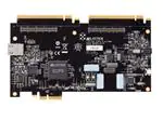


 工商网监
湘ICP备2023018690号
工商网监
湘ICP备2023018690号
