LatticeSC/M Family Data Sheet
DS1004 Version 02.4, December 2011
�LatticeSC/M Family Data Sheet
Introduction
January 2010
Data Sheet DS1004
Features
High Performance FPGA Fabric
• 15K to 115K four input Look-up Tables (LUT4s)
• 139 to 942 I/Os
• 700MHz global clock; 1GHz edge clocks
4 to 32 High Speed SERDES and flexiPCS™
(per Device)
• Performance ranging from 600Mbps to 3.8Gbps
• Excellent Rx jitter tolerance (0.8UI at
3.125Gbps)
• Low Tx jitter (0.25UI typical at 3.125Gbps)
• Built-in Pre-emphasis and equalization
• Low power (typically 105mW per channel)
• Embedded Physical Coding Sublayer (PCS)
provides pre-engineered implementation for the
following standards:
– GbE, XAUI, PCI Express, SONET, Serial RapidIO, 1G Fibre Channel, 2G Fibre Channel
2Gbps High Performance PURESPEED™ I/O
• Supports the following performance bandwidths
– Differential I/O up to 2Gbps DDR
(1GHz Clock)
– Single-ended memory interfaces up to
800Mbps
• 144 Tap programmable Input Delay (INDEL)
block on every I/O dynamically aligns data to
clock for robust performance
– Dynamic bit Adaptive Input Logic (AIL) monitoring and control circuitry per pin that automatically ensures proper set-up and hold
– Dynamic bus: uses control bus from DLL
– Static per bit
• Electrical standards supported:
– LVCMOS 3.3/2.5/1.8/1.5/1.2, LVTTL
– SSTL 3/2/18 I, II; HSTL 18/15 I, II
– PCI, PCI-X
– LVDS, Mini-LVDS, Bus-LVDS, MLVDS,
LVPECL, RSDS
• Programmable On Die Termination (ODT)
– Includes Thevenin Equivalent and low
power VTT termination options
Memory Intensive FPGA
• sysMEM™ embedded Block RAM
– 1 to 7.8 Mbits memory
– True Dual Port/Pseudo Dual Port/Single
Port
– Dedicated FIFO logic for all block RAM
– 500MHz performance
• Additional 240K to 1.8Mbits distributed RAM
sysCLOCK™ Network
• Eight analog PLLs per device
– Frequency range from 15MHz to 1GHz
– Spread spectrum support
• 12 DLLs per device with direct control of I/O
delay
– Frequency range from 100MHz to 700MHz
• Extensive clocking network
– 700MHz primary and 325 MHz secondary
clocks
– 1GHz I/O-connected edge clocks
• Precision Clock Divider
– Phase matched x2 and x4 division of incoming clocks
• Dynamic Clock Select (DCS)
– Glitch free clock MUX
Masked Array for Cost Optimization
(MACO™) Blocks
• On-chip structured ASIC Blocks provide preengineered IP for low power, low cost system
level integration
High Performance System Bus
• Ties FPGA elements together with a standard
bus framework
– Connects to peripheral user interfaces for
run-time dynamic configuration
System Level Support
• IEEE standard 1149.1 Boundary Scan, plus
ispTRACY™ internal logic analyzer
• IEEE Standard 1532 in-system configuration
• 1.2V and 1.0V operation
• Onboard oscillator for initialization and general
use
• Embedded PowerPC microprocessor interface
• Low cost wire-bond and high pin count flip-chip
packaging
• Low cost SPI Flash RAM configuration
© 2010 Lattice Semiconductor Corp. All Lattice trademarks, registered trademarks, patents, and disclaimers are as listed at www.latticesemi.com/legal. All other brand
or product names are trademarks or registered trademarks of their respective holders. The specifications and information herein are subject to change without notice.
www.latticesemi.com
1-1
DS1004 Introduction_01.7
�Introduction
LatticeSC/M Family Data Sheet
Lattice Semiconductor
Table 1-1. LatticeSC Family Selection Guide1
Device
SC15
SC25
SC40
SC80
SC115
LUT4s (K)
15
25
40
80
115
sysMEM Blocks (18Kb)
56
104
216
308
424
Embedded Memory (Mbits)
1.03
1.92
3.98
5.68
7.8
Max. Distributed Memory (Mbits)
0.24
0.41
0.65
1.28
1.84
Number of 3.8Gbps SERDES (Max.)
8
16
16
32
32
DLLs
12
12
12
12
12
Analog PLLs
8
8
8
8
8
MACO Blocks
4
6
10
10
12
660/16
660/16
904/32
942/32
Package I/O/SERDES Combinations (1mm ball pitch)
256-ball fpBGA (17 x 17mm)
139/4
900-ball fpBGA (31 x 31mm)
300/8
1020-ball fcBGA (33 x 33mm)2
1152-ball fcBGA (35 x 35mm)
378/8
476/16
3
562/16
604/16
1704-ball fcBGA (42.5 x 42.5mm)3
1. The information in this preliminary data sheet is by definition not final and subject to change. Please consult the Lattice web site and your
local Lattice sales office to ensure you have the latest information regarding the specifications for these products as you make critical
design decisions.
2. Organic fcBGA converted to organic fcBGA revision 2 per PCN #02A-10.
3. Ceramic fcBGA converted to organic fcBGA per PCN #01A-10.
The LatticeSCM devices add MACO-enabled IP functionality to the base LatticeSC devices. Table 1-2 shows the
type and number of each pre-engineered IP core.
Table 1-2. LatticeSCM Family
Device
SCM15
SCM25
SCM40
SCM80
SCM115
flexiMAC Blocks
• 1GbE Mode
• 10GbE Mode
• PCI Express Mode
1
2
2
2
4
SPI4.2 Blocks
1
2
2
2
2
Memory Controller Blocks
• DDR/DDR2 DRAM Mode
• QDR II/II+ SRAM Mode
• RLDRAM I
• RLDRAM II CIO/SIO
1
2
2
2
2
Low-Speed CDR Blocks
0
0
2
2
2
PCI Express LTSSM (PHY) Blocks
1
0
2
2
2
Note: See each IP core user’s guide for more information about support for specific LatticeSCM devices.
Introduction
The LatticeSC family of FPGAs combines a high-performance FPGA fabric, high-speed SERDES, high-performance I/Os and large embedded RAM in a single industry leading architecture. This FPGA family is fabricated in a
state of the art technology to provide one of the highest performing FPGAs in the industry.
This family of devices includes features to meet the needs of today’s communication network systems. These features include SERDES with embedded advance PCS (Physical Coding sub-layer), up to 7.8 Mbits of sysMEM
embedded block RAM, dedicated logic to support system level standards such as RAPIDIO, SPI4.2, SFI-4, UTOPIA, XGMII and CSIX. The devices in this family feature clock multiply, divide and phase shift PLLs, numerous
1-2
�Introduction
LatticeSC/M Family Data Sheet
Lattice Semiconductor
DLLs and dynamic glitch free clock MUXs which are required in today’s high end system designs. High-speed,
high-bandwidth I/O make this family ideal for high-throughput systems.
The ispLEVER® design tool from Lattice allows large complex designs to be efficiently implemented using the LatticeSC family of FPGA devices. Synthesis library support for LatticeSC is available for popular logic synthesis tools.
The ispLEVER tool uses the synthesis tool output along with the constraints from its floor planning tools to place
and route the design in the LatticeSC device. The ispLEVER tool extracts the timing from the routing and backannotates it into the design for timing verification.
Lattice provides many pre-designed IP (Intellectual Property) ispLeverCORE™ modules for the LatticeSC family.
By using these IPs as standardized blocks, designers are free to concentrate on the unique aspects of their design,
increasing their productivity.
Innovative high-performance FPGA architecture, high-speed SERDES with PCS support, sysMEM embedded
memory and high performance I/O are combined in the LatticeSC to provide excellent performance for today’s
leading edge systems designs. Table 1-3 details the performance of several common functions implemented within
the LatticeSC.
Table1-3. Speed Performance for Typical Functions1
Performance (MHz)2
Functions
32-bit Address Decoder
539
64-bit Address Decoder
517
32:1 Multiplexer
779
64-bit Adder (ripple)
353
32x8 Distributed Single Port (SP) RAM
768
64-bit Counter (up or down counter, non-loadable)
369
True Dual-Port 1024x18 bits
372
FIFO Port A: x36 bits, B: x9 bits
375
1. For additional information, see Typical Building BLock Function Performance table
in this data sheet.
2. Advance information (-7 speed grade).
1-3
�LatticeSC/M Family Data Sheet
Architecture
December 2008
Data Sheet DS1004
Architecture Overview
The LatticeSC architecture contains an array of logic blocks surrounded by Programmable I/O Cells (PIC). Interspersed between the rows of logic blocks are rows of sysMEM Embedded Block RAM (EBR). The upper left and
upper right corners of the devices contain SERDES blocks and their associated PCS blocks, as show in Figure 2-1.
Top left and top right corner of the device contain blocks of SERDES. Each block of SERDES contains four channels (quad). Each channel contains a single serializer and de-serializer, synchronization and word alignment logic.
The SERDES quad connects with the Physical Coding Sub-layer (PCS) blocks that contain logic to simultaneously
perform alignment, coding, de-coding and other functions. The SERDES quad block has separate supply, ground
and reference voltage pins.
The PICs contain logic to facilitate the conditioning of signals to and from the I/O before they leave or enter the
FPGA fabric. The block provides DDR and shift register capabilities that act as a gearbox between high speed I/O
and the FPGA fabric. The blocks also contain programmable Adaptive Input Logic that adjusts the delay applied to
signals as they enter the device to optimize setup and hold times and ensure robust performance.
sysMEM EBRs are large dedicated fast memory blocks. They can be configured as RAM, ROM or FIFO. These
blocks have dedicated logic to simplify the implementation of FIFOs.
The PFU, PIC and EBR blocks are arranged in a two-dimensional grid with rows and columns as shown in
Figure 2-1. These blocks are connected with many vertical and horizontal routing channel resources. The place
and route software tool automatically allocates these routing resources.
The corners contain the sysCLOCK Analog Phase Locked Loop (PLL) and Delay Locked Loop (DLL) Blocks. The
PLLs have multiply, divide and phase shifting capability; they are used to manage the phase relationship of the
clocks. The LatticeSC architecture provides eight analog PLLs per device and 12 DLLs. The DLLs provide a simple
delay capability and can also be used to calibrate other delays within the device.
Every device in the family has a JTAG Port with internal Logic Analyzer (ispTRACY) capability. The sysCONFIG™
port which allows for serial or parallel device configuration. The system bus simplifies the connections of the external microprocessor to the device for tasks such as SERDES and PCS configuration or interface to the general
FPGA logic. The LatticeSC devices use 1.2V as their core voltage operation with 1.0V operation also possible.
© 2008 Lattice Semiconductor Corp. All Lattice trademarks, registered trademarks, patents, and disclaimers are as listed at www.latticesemi.com/legal. All other brand
or product names are trademarks or registered trademarks of their respective holders. The specifications and information herein are subject to change without notice.
www.latticesemi.com
2-1
DS1004 Architecture_02.0
�Architecture
LatticeSC/M Family Data Sheet
Lattice Semiconductor
Figure 2-1. Simplified Block Diagram (Top Level)
Quad SERDES
Quad SERDES
sysCLOCK
Analog PLLs
Physical Coding
Sublayer (PCS)
sysCLOCK DLLs
Programmable
I/O Cell (PIC) includes
PURESPEED I/O Interface
Structured ASIC
Block (MACO)
Programmable
Function
Unit (PFU)
Each PIC
contains four
Programmable
I/Os (PIO)
sysMEM Embedded
Block RAM (EBR)
Three PICs
per four PFUs
sysCLOCK
Analog PLLs
sysCLOCK DLLs
2-2
�Architecture
LatticeSC/M Family Data Sheet
Lattice Semiconductor
PFU Blocks
The core of the LatticeSC devices consists of PFU blocks. The PFUs can be programmed to perform Logic, Arithmetic, Distributed RAM and Distributed ROM functions.
Each PFU block consists of four interconnected slices, numbered 0-3 as shown in Figure 2-2. All the interconnections to and from PFU blocks are from routing. There are 53 inputs and 25 outputs associated with each PFU block.
Figure 2-2. PFU Diagram
From
Routing
LUT4 &
CARRY
LUT4 &
CARRY
LUT4 &
CARRY
Slice 0
D
FF/
Latch
D
FF/
Latch
LUT4 &
CARRY
LUT4 &
CARRY
Slice 1
D
FF/
Latch
LUT4 &
CARRY
LUT4 &
CARRY
Slice 3
Slice 2
D
FF/
Latch
D
FF/
Latch
LUT4 &
CARRY
D
FF/
Latch
D
FF/
Latch
D
FF/
Latch
To
Routing
Slice
Each slice contains two LUT4 lookup tables feeding two registers (programmed to be in FF or Latch mode), and
some associated logic that allows the LUTs to be combined to implement 5, 6, 7 and 8 Input LUTs (LUT5, LUT6,
LUT7 and LUT8). There is control logic to perform set/reset functions (programmable as synchronous/asynchronous), clock select, chip-select and wider RAM/ROM functions. Figure 2-3 shows an overview of the internal logic
of the slice. The registers in the slice can be configured for positive/negative and edge/level clocks.
There are 14 input signals: 13 signals from routing and one from the carry-chain (from adjacent slice or PFU).
There are seven outputs: six to routing and one to carry-chain (to adjacent PFU). Table 2-1 lists the signals associated with each slice.
2-3
�Architecture
LatticeSC/M Family Data Sheet
Lattice Semiconductor
Figure 2-3. Slice Diagram
FCO from Slice/PFU,
FCI into Different Slice/PFU
Slice
OFX1
A1
B1
C1
D1
CO
F1
F
Q1
D
LUT4 &
CARRY
FF/
Latch
CI
From
Routing
To
Routing
M1
M0
OFX0
LUT
Expansion
Mux
CO
A0
B0
C0
D0
LUT4 &
CARRY
F0
F
OFX0
FF/
Latch
CI
Control Signals
selected and
inverted per
slice in routing
Q0
D
CE
CLK
LSR
FCI into Slice/PFU,
FCO from Different Slice/PFU
Note: some interslice
signals not shown.
Table 2-1. Slice Signal Descriptions
Function
Type
Input
Data signal
A0, B0, C0, D0 Inputs to LUT4
Signal Names
Description
Input
Data signal
A1, B1, C1, D1 Inputs to LUT4
Input
Multi-purpose
M0
Multipurpose Input
Input
Multi-purpose
M1
Multipurpose Input
Input
Control signal
CE
Clock Enable
Input
Control signal
LSR
Local Set/Reset
Input
Control signal
CLK
System Clock
Input
Inter-PFU signal
FCI
Fast Carry In1
Output
Data signals
F0, F1
LUT4 output register bypass signals
Output
Data signals
Q0, Q1
Register Outputs
Output
Data signals
OFX0
Output of a LUT5 MUX
Output
Data signals
OFX1
Output of a LUT6, LUT7, LUT82 MUX depending on the slice
Output
Inter-PFU signal
FCO
For the right most PFU the fast carry chain output2
1. See Figure 2-2 for connection details.
2. Requires two PFUs.
2-4
�Architecture
LatticeSC/M Family Data Sheet
Lattice Semiconductor
Modes of Operation
Each Slice is capable of four modes of operation: Logic, Ripple, RAM and ROM. Table 2-2 lists the modes and the
capability of the Slice blocks.
Table 2-2. Slice Modes
Logic
PFU Slice
LUT 4x2 or LUT 5x1
Ripple
RAM
ROM
2-bit Arithmetic Unit
SPR 16x2
DPR 16x2
ROM 16x2
Logic Mode
In this mode, the LUTs in each Slice are configured as combinatorial lookup tables. A LUT4 can have 16 possible
input combinations. Any logic function with four inputs can be generated by programming this lookup table. Since
there are two LUT4s per Slice, a LUT5 can be constructed within one Slice. Larger lookup tables such as LUT6,
LUT7 and LUT8 can be constructed by concatenating other Slices in the PFU.
Ripple Mode
Ripple mode allows the efficient implementation of small arithmetic functions. In ripple mode, the following functions can be implemented by each Slice:
Addition 2-bit
Subtraction 2-bit
Up counter 2-bit
Down counter 2-bit
Comparator functions of A and B inputs
- A greater-than-or-equal-to B
- A not-equal-to B
- A less-than-or-equal-to B
Ripple Mode includes an optional configuration that performs arithmetic using fast carry chain methods. In this configuration (also referred to as CCU2 mode) two additional signals, Carry Generate and Carry Propagate, are generated on a per slice basis to allow fast arithmetic functions to be constructed by concatenating Slices.
RAM Mode
In this mode, distributed RAM can be constructed using each LUT block as a 16x1-bit memory. Through the combination of LUTs and Slices, a variety of different memories can be constructed.
The Lattice design tools support the creation of a variety of different size memories. Where appropriate, the software will construct these using distributed memory primitives that represent the capabilities of the Slice. Table 2-3
shows the number of Slices required to implement different distributed RAM primitives. Dual port memories involve
the pairing of two Slices, one Slice functions as the read-write port. The other companion Slice supports the readonly port. For more information on RAM mode, please see details of additional technical documentation at the end
of this data sheet.
Table 2-3. Number of Slices Required For Implementing Distributed RAM
SPR16x2
DPR16x2
1
2
Number of Slices
Note: SPR = Single Port RAM, DPR = Dual Port RAM
ROM Mode
The ROM mode uses the same principal as the RAM modes, but without the Write port. Pre-loading is accomplished through the programming interface during configuration.
2-5
�Architecture
LatticeSC/M Family Data Sheet
Lattice Semiconductor
PFU Modes of Operation
Slices can be combined within a PFU to form larger functions. Table 2-4 tabulates these modes and documents the
functionality possible at the PFU level.
Table 2-4. PFU Modes of Operation
Ripple
RAM
ROM
LUT 4x8 or
MUX 2x1 x 8
Logic
2-bit Add x 4
SPR 16x2 x 4
DPR 16x2 x 2
ROM 16x1 x 8
LUT 5x4 or
MUX 4x1 x 4
2-bit Sub x 4
SPR 16x4 x 2
DPR 16x4 x 1
ROM 16x2 x 4
LUT 6x2 or
MUX 8x1 x 2
2-bit Counter x 4
SPR 16x8 x 1
ROM 16x4 x 2
LUT 7x1 or
MUX 16x1 x 1
2-bit Comp x 4
ROM 16x8 x1
Routing
There are many resources provided in the LatticeSC devices to route signals individually or as busses with related
control signals. The routing resources consist of switching circuitry, buffers and metal interconnect (routing) segments.
The inter-PFU connections are made with x1 (spans two PFU), x2 (spans three PFU) and x6 (spans seven PFU)
resources. The x1 and x2 connections provide fast and efficient connections in horizontal, vertical and diagonal
directions. All connections are buffered to ensure high-speed operation even with long high-fanout connections.
The ispLEVER design tool takes the output of the synthesis tool and places and routes the design. Generally, the
place and route tool is completely automatic, although an interactive routing editor is available to optimize the
design.
sysCLOCK Network
The LatticeSC devices have three distinct clock networks for use in distributing high-performance clocks within the
device: primary clocks, secondary clocks and edge clocks. In addition to these dedicated clock networks, users are
free to route clocks within the device using the general purpose routing. Figure 2-4 shows the clock resources
available to each slice.
Figure 2-4. Slice Clock Selection
Primary Clock
Secondary Clock
12
6
Clock to Slice
Routing
GND
Note: GND is available to switch off the network.
Primary Clock Sources
LatticeSC devices have a wide variety of primary clock sources available. Primary clocks sources consists of the
following:
• Primary clock input pins
• Edge clock input pins
• Two outputs per DLL
2-6
�Architecture
LatticeSC/M Family Data Sheet
Lattice Semiconductor
•
•
•
•
Two outputs per PLL
Clock divider outputs
Digital Clock Select (DCS) block outputs
Three outputs per SERDES quad
Figure 2-5 shows the arrangement of the primary clock sources.
Figure 2-5. Clock Sources
Primary/
Edge Clock
PIOs
Edge
Clock
PIOs
PLL
PLL
PLL
DLL
Primary/
Edge Clock
PIOs
SERDES
PLL
SERDES
DCS
DCS
Clock Dividers (3 per SERDES Channel)
(3 per SERDES Channel)
DLL
Primary/
Edge Clock
PIOs
DLL
DLL
4
Edge Clock
PIOs
Edge Clock
PIOs
DCS
DCS
Primary Clock Sources
24
DCS
Primary/
Edge Clock
PIOs
24
Clock
Dividers
DCS
Clock
Dividers
DLL
DLL
DLL
DLL
8
DLL
DLL
DLL
DLL
PLL
Primary/
Edge Clock
PIOs
Clock Dividers
DCS
DCS
Clock Dividers
PLL
PLL
PLL
Edge
Clock
PIOs
Primary/
Edge Clock
PIOs
Edge
Clock
PIOs
Primary/
Edge Clock
PIOs
Primary Clock Routing
The clock routing structure in LatticeSC devices consists of 12 Primary Clock lines per quadrant. The primary
clocks are generated from 64:1 MUXs located in each quadrant. Three of the inputs to each 64:1 MUX comes from
local routing, one is connected to GND and rest of the 60 inputs are from the primary clock sources. Figure 2-6
shows this clock routing.
2-7
�Architecture
LatticeSC/M Family Data Sheet
Lattice Semiconductor
Figure 2-6. Per Quadrant Clock Selection
12 feedlines per quadrants
4 + Clock
12 feedlines
60times
Primary
Sourcesfrom upper and lower half
From Local
Routing
3
From Local
Routing
60
GND
3
From Local
Routing
60
GND
3
60
GND
12 Primary
12 Primary
Clock per
Clocks
Quadrants
Note: GND is available to switch off the network.
Secondary Clocks
In addition to the primary clock network and edge clocks the LatticeSC devices also contain a secondary clock network. Built of X6 style routing elements this secondary clock network is ideal for routing slower speed clock and
control signals throughout the device preserving high-speed clock networks for the most timing critical signals.
Edge Clocks
LatticeSC devices have a number of high-speed edge clocks that are intended for use with the PIOs in the implementation of high-speed interfaces. There are eight edge clocks per bank for the top and bottom of the device. The
left and right sides have eight edge clocks per side for both banks located on that side. Figure 2-7 shows the
arrangement of edge clocks.
Edge clock resources can be driven from a variety of sources. Edge clock resources can be driven from:
•
•
•
•
•
Edge clock PIOs in the same bank
Primary clock PIOs in the same bank
Routing
Adjacent PLLs and DLLs
ELSR output from the clock divider
2-8
�Architecture
LatticeSC/M Family Data Sheet
Lattice Semiconductor
Figure 2-7. Edge Clock Resources
Bank 1
SERDES
SERDES
Bank 2
Bank 7
Edge clock
Bank 3
Bank 6
Bank 5
Bank 4
Precision Clock Divider
Each set of edge clocks has four high-speed dividers associated with it. These are intended for generating a slower
speed system clock from the high-speed edge clock. The block operates in a DIV2 or DIV4 mode and maintains a
known phase relationship between the divided down clock and high-speed clock based on the release of its reset
signal. The clock dividers can be fed from selected PIOs, PLLs and routing. The clock divider outputs serve as primary clock sources. This circuit also generates an edge local set/reset (ELSR) signal which is fed to the PIOs via
the edge clock network and is used for the rest of the I/O gearing logic.
Figure 2-8. Clock Divider Circuit
Divided clock
S/R
S/R
S/R
S/R
Clock derived
from selected
PIOs, PLLs and
routing
ELSR
LSR
Register chain to synchronize LSR to clock input
Dynamic Clock Select (DCS)
The DCS is a global clock buffer with smart multiplexer functions. It takes two independent input clock sources and
outputs a clock signal without any glitches or runt pulses. This is achieved irrespective of where the select signal is
2-9
�Architecture
LatticeSC/M Family Data Sheet
Lattice Semiconductor
toggled. There are eight DCS blocks per device, located in pairs at the center of each side. Figure 2-9 illustrates
the DCS Block diagram.
Figure 2-9. DCS Block Diagram
CLK0
CLK1
DCS
DCSOUT
SEL
Figure 2-10 shows timing waveforms for one of the DCS operating modes. The DCS block can be programmed to
other modes. For more information on the DCS, please see details of additional technical documentation at the end
of this data sheet.
Figure 2-10. DCS Waveforms
CLK0
CLK1
SEL
DCSOUT
Clock Boosting
There are programmable delays available in the clock signal paths in the PFU, PIC and EBR blocks. These allow
setup and clock-to-output times to be traded to meet critical timing without slowing the system clock. If this feature
is enabled then the design tool automatically uses these delays to improve timing performance.
Global Set/Reset
There is a global set/reset (GSR) network on the device that is distributed to all FFs, PLLs, DLLs and other blocks
on the device. This GSR network can operate in two modes:
a) asynchronous - no clock is required to get into or out of the reset state.
b) synchronous - The global GSR net is synchronized to a user selected clock. In this mode it continues to be
asynchronous to get into the reset state, but is synchronous to get out of the reset state. This allows all registers on the device to become operational in the same clock period. The synchronous GSR goes out of
reset in two cycles from the clock edge where the setup time of the FF was met (not from the GSR being
released).
sysCLOCK Phase Locked Loops (PLLs)
The sysCLOCK PLLs provide the ability to synthesize clock frequencies. Each PLL has four dividers associated
with it: input clock divider, feedback divider and two clock output dividers. The input divider is used to divide the
input clock signal, while the feedback divider is used to multiply the input clock signal.
2-10
�Architecture
LatticeSC/M Family Data Sheet
Lattice Semiconductor
The setup and hold times of the device can be improved by programming a delay in the feedback or input path of
the PLL which will advance or delay the output clock with reference to the input clock. This delay can be either programmed during configuration or can be adjusted dynamically.
The Phase Select block can modify the phase of the clock signal if desired. The Spread Spectrum block supports
the modulation of the PLL output frequency. This reduces the peak energy in the fundamental and its harmonics
providing for lower EMI (Electro Magnetic Interference).
The sysCLOCK PLL can be configured at power-up and then, if desired, reconfigured dynamically through the
serial memory interface bus which connects with the on-chip system bus. For example, the user can select inputs,
loop filters, divider setting, delay settings and phase shift settings. The user can also directly access the SMI bus
through the routing.
The PLL clock input, from pin or routing, feeds into an input divider. There are four sources of feedback signal to
the feedback divider: from the clock net, directly from the voltage controlled oscillator (VCO) output, from the routing or from an external pin. The signal from the input clock divider and the feedback divider are passed through the
programmable delay before entering the phase frequency detector (PFD) unit. The output of this PFD is used to
control the voltage controlled oscillator. There is a PLL_LOCK signal to indicate that VCO has locked on to the
input clock signal. Figure 2-11 shows the sysCLOCK PLL diagram.
Figure 2-11. PLL Diagram
CLKOP
CLKI
Div
Div
Prog
Delay
PFD
CLKFB
Div
RSTN
VCO/
Loop Filter
Phase
Adjust
Prog
Delay
Prog
Delay
Div
CLKOS
Optional Internal Feedback
From PFD
LOCK
For more information on the PLL, please see details of additional technical documentation at the end of this data
sheet.
Spread Spectrum Clocking (SSC)
The PLL supports spread spectrum clocking to reduce peak EMI by using “down-spread” modulation. The spread
spectrum operation will vary the output frequency (at 30KHz to 500KHz) in a range that is between its nominal
value, down to a frequency that is a programmable 1%, 2%, or 3% lower than normal.
Digital Locked Loop (DLLs)
In addition to PLLs, the LatticeSC devices have up to 12 DLLs per device. DLLs assist in the management of clocks
and strobes. DLLs are well suited to applications where the clock may be stopped or transferring jitter from input to
output is important, for example forward clocked interfaces. PLLs are good for applications requiring the lowest output jitter or jitter filtering. All DLL outputs are routed as primary/edge clock sources.
The DLL has two independent clock outputs, CLKOP and CLKOS. These outputs can individually select one of the
outputs from the tapped delay line. The CLKOS has optional fine phase shift and divider blocks to allow this output
to be further modified, if required. The fine phase shift block allows the CLKOS output to phase shifted a further 45,
22.5 or 11.25 degrees relative to its normal position. LOCK output signal is asserted when the DLL is locked. The
ALU HOLD signal setting allows users to freeze the DLL at its current delay setting.
2-11
�Architecture
LatticeSC/M Family Data Sheet
Lattice Semiconductor
There is a Digital Control (DCNTL) bus available from the DLL block. This Digital Control bus is available to the
delay lines in the PIC blocks in the adjacent banks. The UDDCNTL signal allows the user to latch the current value
on the digital control bus.
Figure 2-12 shows the DLL block diagram of the DLL inputs and outputs. The output of the phase frequency detector controls an arithmetic logic unit (ALU) to add or subtract one delay tap. The digital output of this ALU is used to
control the delay value of the delay chain and this digital code is transmitted via the DCNTL bus.
The sysCLOCK DLL can be configured at power-up, then, if desired, reconfigured dynamically through the Serial
Memory Interface bus which interfaces with the on-chip Microprocessor Interface (MPI) bus. In addition, users can
drive the SMI interface from routing if desired.
The user can configure the DLL for many common functions such as clock injection match and single delay cell.
Lattice provides primitives in its design for time reference delay (DDR memory) and clock injection delay removal.
Figure 2-12. DLL Diagram
CLKI
PFD
Phase Adj
Duty50
Phase Adj
Duty50
Delay
Chain
CLKFB
ALU
CLKOP
CLKOS
LOCK
ALUHOLD
DCNTL
Gen
UDDCNTL
DCNTL
RSTN
PLL/DLL Cascading
The LatticeSC devices have been designed to allow certain combinations of PLL and DLL cascading. The allowable combinations are as follows:
•
•
•
•
PLL to PLL
PLL to DLL
DLL to DLL
DLL to PLL
DLLs are used to shift the clock in relation to the data for source synchronous inputs. PLLs are used for frequency
synthesis and clock generation for source synchronous interfaces. Cascading PLL and DLL blocks allows applications to utilize the unique benefits of both DLL and PLLs.
When cascading the DLL to the PLL, the DLL can be used to drive the PLL to create fine phase shifts of an input
clock signal. Figure 2-13 shows a shift of all outputs for CLKOP and CLKOS out in time.
2-12
�Architecture
LatticeSC/M Family Data Sheet
Lattice Semiconductor
Figure 2-13. DLL to PLL
CLKOP
CLKI
DLL
CLKOS
PLL
CLKOS
SMI Bus
Figure 2-14 shows a shift of only CLKOP out in time.
Figure 2-14. PLL to DLL
CLKI
PLL
CLKOP
DLL
CLKOS
SMI Bus
Figure 2-15 shows a shift of only CLKOS out in time.
Figure 2-15. PLL to DLL
CLKI
PLL
CLKOS
DLL
CLKOS
SMI Bus
For further information on the DLL, please see details of additional technical documentation at the end of this data
sheet.
sysMEM Memory Block
The sysMEM block can implement single port, true dual port, pseudo dual port or FIFO memories. Dedicated FIFO
support logic allows the LatticeSC devices to efficiently implement FIFOs without consuming LUTs or routing
resources for flag generation. Each block can be used in a variety of depths and widths as shown in Table 2-5.
Memory with ranges from x1 to x18 in all modes: single port, pseudo-dual port and FIFO also providing x36.
2-13
�Architecture
LatticeSC/M Family Data Sheet
Lattice Semiconductor
Table 2-5. sysMEM Block Configurations
Memory Mode
Configurations
Single Port
16,384 x 1
8,192 x 2
4,096 x 4
2,048 x 9
1,024 x 18
512 x 36
True Dual Port
16,384 x 1
8,192 x 2
4,096 x 4
2,048 x 9
1,024 x 18
Pseudo Dual Port
16,384 x 1
8,192 x 2
4,096 x 4
2,048 x 9
1,024 x 18
512 x 36
FIFO
16,384 x 1
8,192 x 2
4,096 x 4
2,048 x 9
1,024 x 18
512 x 36
Bus Size Matching
All of the multi-port memory modes support different widths on each of the ports. The RAM bits are mapped LSB
word 0 to MSB word 0, LSB word 1 to MSB word 1 and so on. Although the word size and number of words for
each port varies, this mapping scheme applies to each port.
RAM Initialization and ROM Operation
If desired, the contents of the RAM can be pre-loaded during device configuration. By preloading the RAM block
during the chip configuration cycle and disabling the write controls, the sysMEM block can also be utilized as a
ROM.
Single, Dual and Pseudo-Dual Port Modes
In all the sysMEM RAM modes the input data and address for the ports are registered at the input of the memory
array. The output data of the memory is optionally registered at the output. A clock is required even in asynchronous read mode.
The EBR memory supports two forms of write behavior for dual port operation:
1. Normal — data on the output appears only during a read cycle. During a write cycle, the data (at the current
address) does not appear on the output.
2. Write Through — a copy of the input data appears at the output of the same port.
FIFO Configuration
The FIFO has a write port with Data-in, WCE, WE and WCLK signals. There is a separate read port with Data-out,
RCE, RE and RCLK signals. The FIFO internally generates Almost Full, Full, Almost Empty, and Empty Flags. The
Full and Almost Full flags are registered with WCLK. The Empty and Almost Empty flags are registered with RCLK.
2-14
�Architecture
LatticeSC/M Family Data Sheet
Lattice Semiconductor
EBR Asynchronous Reset
EBR asynchronous reset or GSR (if used) can only be applied if all clock enables are low for a clock cycle before the
reset is applied and released a clock cycle after the low-to-high transition of the reset, as shown in Figure 2-16.
Figure 2-16. EBR Asynchronous Reset (Including GSR) Timing Diagram
Reset
Clock
Clock
Enable
If all clock enables remain enabled, the EBR asynchronous reset or GSR may only be applied and released after
the EBR read and write clock inputs are in a steady state condition for a minimum of 1/fMAX (EBR clock). The reset
release must adhere to the EBR synchronous reset setup time before the next active read or write clock edge.
If an EBR is pre-loaded during configuration, the GSR input must be disabled or the release of the GSR during
device Wake Up must occur before the release of the device I/Os becoming active.
These instructions apply to all EBR RAM, ROM, FIFO and shift register implementations. For the EBR FIFO mode,
the GSR signal is always enabled and the WE and RE signals act like the clock enable signals in Figure 2-16. The
reset timing rules apply to the RPReset input vs. the RE input and the RST input vs. the WE and RE inputs. Both
RST and RPReset are always asynchronous EBR inputs. For the EBR shift register mode, the GSR signal is
always enabled and the local RESET pin is always asynchronous.
Note that there are no reset restrictions if the EBR synchronous reset is used and the EBR GSR input is disabled.
For more information about on-chip memory, see TN1094, On-Chip Memory Usage Guide for LatticeSC Devices.
Programmable I/O Cells (PIC)
Each PIC contains four PIOs connected to their respective PURESPEED I/O Buffer which are then connected to
the PADs as shown in Figure 2-17. The PIO Block supplies the output data (DO) and the Tri-state control signal
(TO) to PURESPEED I/O buffer, and receives input (DI) from the buffer. The PIO contains advanced capabilities to
allow the support of speeds up to 2Gbps. These include dedicated shift and DDR logic and adaptive input logic.
The dedicated resources simplify the design of robust interfaces.
2-15
�Architecture
LatticeSC/M Family Data Sheet
Lattice Semiconductor
Figure 2-17. PIC Diagram
PIO A
TD
Tristate
Register Block
IOLT0
DO
TO
OPOS0
ONEG0
OPOS1
ONEG1
OPOS2
ONEG2
OPOS3
ONEG3
PADA
"T"
Output
Register Block
DO
PURESPEED
I/O Buffer
INCK
INDD
INFF
IPOS0
INEG0
IPOS1
INEG1
IPOS2
INEG2
IPOS3
INEG3
RUNAIL
LOCK
CLK
CE
LSR
GSRN
ELSR
ECLK
DI
DI
Input
Register Block
(including
delay and
AIL elements*)
HCLKOUT
LCLKOUT
CEO
LSRO
GSR
LSRO
HCLKIN
LCLKIN
Control
Muxes
UPDATE
Update Block
POS Update
NEG Update
PIO B
PADB
“C”
PIO C
PADC
“T”
PIO D
PADD
“C”
*AIL only on A or C pads located on the left, right and bottom of the device.
The A/B PIOs on the left and the right of the device can be paired to form a differentiated driver. The A/B and C/D
PIOs on all sides of the device can be paired to form differential receivers. Either A or C PIOs on all sides except
the one on top also provide a connection to an adaptive input logic capability that facilitates the implementation of
2-16
�Architecture
LatticeSC/M Family Data Sheet
Lattice Semiconductor
high-speed interfaces in the LatticeSC devices. Figure 2-18 shows how differential receivers and drivers are
arranged between PIOs.
Figure 2-18. Differential Drivers and Receivers
PIO A
PADA "T"
PIO B
PADB "C"
PIO C
PADC "T"
PIO D
PADD "C"
*Differential Driver only available on right and left of the device.
PIO
The PIO contains five blocks: an input register block, output register block, tristate register block, update block, and
a control logic block. These blocks contain registers for both single data rate (SDR), double data rate (DDR), and
shift register operation along with the necessary clock and selection logic.
Input Register Block
The input register block contains delay elements and registers that can be used to condition signals before they are
passed to the device core. Figure 2-20 show the diagram of the input register block. The signal from the PURESPEED I/O buffer (DI) enters the input register block and can be used for three purposes, as a source for the combinatorial (INDD) and clock outputs (INCK), the input into the SDR register/latch block and the input to the delay
block. The output of the delay block can be used as combinatorial (INDD) and clock (INCK) outputs, an input to the
DDR/Shift Register Block or an input into the SDR register block.
Input SDR Register/Latch Block
The SDR register/latch block has a latch and a register/latch that can be used in a variety of combinations to provide a registered or latched output (INFF). The latch operates off high-speed input clocks and latches data on the
positive going edge. The register/latch operates off the low-speed input clock and registers/latches data on the
positive going edge. Both the latch and the register/latch have a clock enable input that is driven by the input clock
enable. In addition both have a variety of programmable options for set/reset including, set or reset, asynchronous
or synchronous Local Set Reset LSR (LSR has precedence over CE) and Global Set Reset GSR enable or disable.
The register and latch LSR inputs are driven from LSRI, which is generated from the PIO control MUX. The GSR
inputs are driven from the GSR output of the PIO control MUX, which allows the global set-reset to be disabled on
a PIO basis.
Input Delay Block
The delay block uses 144 tapped delay lines to obtain coarse and fine delay resolution. These delays can be
adjusted during configuration or automatically via DLL or AIL blocks. The Adaptive Input Logic (AIL) uses this delay
block to adjust automatically the delay in the data path to ensure that it has sufficient setup and hold time.
The delay line in this block matches the delay line that is used in the 12 on-chip DLLs. The delay line can be set via
configuration bits or driven from a calibration bus that allows the setting to be controlled either from one of the onchip DLLs or user logic. Controlling the delay from one of the on-chip DLLs allow the delay to be calibrated to the
DLL clock and hence compensated for the variations in process, voltage and temperature.
2-17
�Architecture
LatticeSC/M Family Data Sheet
Lattice Semiconductor
Adaptive Input Logic (AIL) Overview
The Adaptive Input Logic (AIL) provides the ability of the input logic to dynamically find a solution by monitoring
multiple samples of the input data. The input data signal from the input buffer is run through a delay chain. Data,
transitions, jitter, noise are all contained inside of the delay chain. The AIL will then search the delay chain for a
clean sampling point for data. Once found the AIL will monitor and walk with the data dynamically. This novel
approach of using a delay chain to create multiple copies of the data provides a lower power solution than oversampling data with a higher speed clock. Figure 2-19 provides a high level view of the AIL methodology.
Figure 2-19. LatticeSC AIL Delay of Input Data Waveform
Input Data Signal
Delay Chain
AIL Acquisition Window
The AIL slides the acquisition window through the delay chain searching for stable data based solely on data transitions. A specific training pattern is not required to perform this bit alignment, simply data transitions. The size of
the acquisition window is user-selectable allowing the AIL to operate over the full range of the PURESPEED I/O
range. Based on dynamic user control the AIL can either continuously adjust the window location based on data
edge detection or it can be locked to a specific delay.
The AIL operates on single data and double data rate interfaces and is available on most FPGA input pins on the
LatticeSC device and all buffer types. The AIL block is low power using only 0.003 mW/MHz typical (6 mW @ 2
Gbps) for PRBS 27 data. Multiple AIL inputs can be used to create a bus with a FPGA circuit to realign the bus to a
common clock cycle. The FPGA circuit to realign the bus is required and is provided by Lattice as a reference
design.
For more information on the LatticeSC AIL please refer to TN1158 LatticeSC PURESPEED I/O Adaptive Input
Logic User’s Guide.
Input DDR/Shift Block
The DDR/Shift block contains registers and associated logic that support DDR and shift register functions using the
high-speed clock and the associated transfer to the low-speed clock domain. It functions as a gearbox allowing
high-speed incoming data to be passed into the FPGA fabric. Each PIO supports DDR and x2 shift functions. If
desired PIOs A and B or C and D can be combined to form x4 shift functions. The PIOs A and C on the left, right
and bottom of the device also contain an optional Adaptive Input Logic (AIL) element. This logic automatically
aligns incoming data with the clock allowing for easy design of high-speed interfaces. Figure 2-21 shows a simplified block diagram of the shift register block. The shift block in conjunction with the update and clock divider blocks
automatically handles the hand off between the low-speed and high-speed clock domains.
2-18
�Architecture
LatticeSC/M Family Data Sheet
Lattice Semiconductor
Figure 2-20. Input Register Block1
CLKENABLE
CLKDISABLE
INDD
INCK
SDR Register/Latch Block
INFF
D-Type/
Latch
Latch
DI
(from
PURESPEED
I/O Buffer)
To
Routing
Delay
Block
Optional
Adaptive
Input
Logic2
DDR/Shift Register Block
• DDR
• DDR + half clock
• DDR + shift x1
• DDR + shift x2
• DDR + shift x43
• Shift x1
• Shift x2
• Shift x43
IPOS0
IPOS1
INEG0
INEG1
LCLKIN (ECLK/SCLK)
HCLKIN (ECLK/SCLK)
LOCK
RUNAIL
DCNTL[0:8]
(From DLL)
1. UPDATE, Set and Reset not shown for clarity
2. Adaptive input logic is only available in selected PIO
3. By four shift modes utilize DDR/shift register block from paired PIO.
4. CLKDISABLE is used to block the transitions on the DQS pin during post-amble. Its main use is to
disable DQS (typically found in DDR memory interfaces) or other clock signals. It can also be used
to disable any/all input signals to save power.
2-19
�Architecture
LatticeSC/M Family Data Sheet
Lattice Semiconductor
Figure 2-21. Input DDR/Shift Register Block
From paired PIO
for wide muxing
To paired PIO
for wide muxing
Bypass used for DDR
IPOS0
(Can act as IPOS2
when paired)
Data Input
(From Delay Block)
IPOS1
(Can act as IPOS3
when paired)
HCLKIN
LCLKIN
POS Update
NEG Update
Bypass used for DDR
INEG0
(Can act as INEG2
when paired)
Used for DDR with
Half Clock Transfer
INEG1
(Can act as INEG3
when paired)
From paired PIO
for wide muxing
To paired PIO
for wide muxing
Output Register Block
The output register block provides the ability to register signals from the core of the device before they are passed
to the PURESPEED I/O buffers. The block contains a register for SDR operation and a group of registers for DDR
and shift register operation. The output signal (DO) can be derived directly from one of the inputs (bypass mode),
the SDR register or the DDR/shift register block. Figure 2-22 shows the diagram of the Output Register Block.
Output SDR Register/Latch Block
The SDR register operates on the positive edge of the high-speed clock. It has clock enable that is driven by the
clock enable output signal generated by the control MUX. In addition it has a variety of programmable options for
set/reset including, set or reset, asynchronous or synchronous Local Set Reset LSR (LSR has precedence over
CE) and Global Set Reset GSR enable or disable. The register LSR input is driven from LSRO, which is generated
from the PIO control MUX. The GSR inputs is driven from the GSR output of the PIO control MUX, which allows the
global set-reset to be disabled on a PIO basis.
Output DDR/Shift Block
The DDR/Shift block contains registers and associated logic that support DDR and shift register functions using the
high-speed clock and the associated transfer from the low-speed clock domain. It functions as a gearbox allowing
low-speed parallel data from the FPGA fabric be output as a higher speed serial stream. Each PIO supports DDR
and x2 shift functions. If desired PIOs A and B or C and D can be combined to form x4 shift functions. Figure 2-22
shows a simplified block diagram of the shift register block.
2-20
�Architecture
LatticeSC/M Family Data Sheet
Lattice Semiconductor
Figure 2-22. Output Register Block1
To
Tri-state
Block
SDR
Register
From
Routing
OPOS0
ONEG0
OPOS1
ONEG1
From
LCLKOUT
Control
HCLKOUT
MUX
DDR/Shift Register Block
• DDR
DO
(to PURESPEED
I/O Buffer)
• DDR + half clock
• DDR + shift x2
• DDR + shift x42
• Shift x2
• Shift x42
Notes:
1. CE, Update, Set and Reset not shown for clarity.
2. By four shift modes utilizes DDR/Shift register block from paired PIO.
3. DDR/Shift register block shared with tristate block.
Figure 2-23. Output/Tristate DDR/Shift Register Block
Bypass Used for
DDR/DDRX Modes
From paired PIO
( x4 shift modes)
To paired PIO
(x4 shift modes)
OPOS0
(Can act as OPOS2
when paired)
Shift x2 / x4
Output
OPOS1
(Can act as OPOS3
when paired)
LCLKOUT
TSDDR/DDRX
HCLKOUT
POS Update
NEG Update
ODDR/DDR/
X2/X4
Bypass Used for
DDR/DDRX Modes
From paired PIO
( x4 shift modes)
ONEG0
(Can act as ONEG2
when paired)
ONEG1
(Can act as ONEG3
when paired)
2-21
To paired PIO
(x4 shift modes)
�Architecture
LatticeSC/M Family Data Sheet
Lattice Semiconductor
Tristate Register Block
The tristate register block provides the ability to register tri-state control signals from the core of the device before
they are passed to the PURESPEED I/O buffers. The block contains a register for SDR operation and a group of
three registers for DDR and shift register operation. The output signal tri-state control signal (TO) can be derived
directly from one of the inputs (bypass mode), the SDR shift register, the DDR registers or the data associated with
the buffer (for open drain emulation). Figure 2-24 shows the diagram of the Tristate Register Block.
Tristate SDR Register/Latch Block
The SDR register operates on the positive edge of the high-speed clock. In it has a variety of programmable
options for set/reset including, set or reset, asynchronous or synchronous Local Set Reset LSR and Global Set
Reset GSR enable or disable. The register LSR input is driven from LSRO, which is generated from the PIO control
MUX. The GSR input is driven from the GSR output of the PIO control MUX, which allows the global set-reset to be
disabled on a PIO basis.
Tristate DDR/Shift Register Block
The DDR/Shift block is shared with the output block allowing DDR support using the high-speed clock and the
associated transfer from the low-speed clock domain. It functions as a gearbox allowing low–speed parallel data
from the FPGA fabric to provide a high-speed tri-state control stream.
There is a special mode for DDR-II memory interfaces where the termination is controlled by the output tristate signal. During WRITE cycle when the FPGA is driving the lines, the parallel terminations are turned off. During READ
cycle when the FPGA is receiving data, the parallel terminations are turned on.
Figure 2-24. Tristate Register Block1
TD
VCC
GND
From
Routing
From
Control
MUX
OPOS1
ONEG1
DDR/Shift Register Block2
• DDR
TO
(To PURESPEED
I/O Buffer)
• DDR + half clock
LCLKOUT
HCLKOUT
Notes:
1. CE, Update, Set and Reset not shown for clarity.
2. DDR/Shift Register Block shared with output register block.
From Output
I/O Architecture Rules
Table 2-6 shows the PIO usage for x1, x2, x4 gearing. The checkmarks in the columns show the specific PIOs that
are used for each gearing mode. When using x2 or x4 gearing, any PIO which is not used for gearing can still be
used as an output.
2-22
�Architecture
LatticeSC/M Family Data Sheet
Lattice Semiconductor
Table 2-6. Input/Output/Tristate Gearing Resource Rules
Input/Output Logic
Tri-State/Bidi
PIO
x1
x2
x4
x1
x2/x4
A
?
?
?
?
N/A
B
?
C
?
D
?
?
N/A
No I/O Logic
?
N/A
No I/O Logic No I/O Logic
?
N/A
No I/O Logic No I/O Logic
?
Note: Pin can still be used without I/O logic.
Control Logic Block
The control logic block allows the modification of control signals selected by the routing before they are used in the
PIO. It can optionally invert all signals passing through it except the Global Set/Reset. Global Set/Reset can be
enabled or disabled. It can route either the edge clock or the clock to the high-speed clock nets. The clock provided
to the PIO by routing is used as the slow-speed clocks. In addition this block contains delays that can be inserted in
the clock nets to enable Lattice’s unique cycle boosting capability.
Update Block
The update block is used to generate the POS update and NEG update signals used by the DDR/Shift register
blocks within the PIO. Note the update block is only required in shift modes. This is required in order to do the high
speed to low speed handoff. One of these update signals is also selected and output from the PIC as the signal
UPDATE. It consists of a shift chain that operates off either the high-speed input or output clock. The values of each
register in the chain are set or reset depending on the desired mode of operation. The set/reset signal is generated
from either the edge reset ELSR or the local reset LSR. These signals are optionally inverted by the Control Logic
Block and provided to the update block as ELSRUP and LSRUP. The Lattice design tools automatically configure
and connect the update block when one of the DDR or shift register primitives is used.
Figure 2-25. Update Block
÷1/2/4
POS Update
NEG Update
HCLKUP
ESLRUP
UPDATE
LSRUP
LCLKUP
PURESPEED I/O Buffer
Each I/O is associated with a flexible buffer referred to as PURESPEED I/O buffer. These buffers are arranged
around the periphery of the device in seven groups referred to as Banks. The PURESPEED I/O buffers allow users
to implement the wide variety of standards that are found in today’s systems including LVCMOS, SSTL, HSTL,
LVDS and LVPECL. The availability of programmable on-chip termination for both input and output use, further
enhances the utility of these buffers.
2-23
�Architecture
LatticeSC/M Family Data Sheet
Lattice Semiconductor
PURESPEED I/O Buffer Banks
LatticeSC devices have seven PURESPEED I/O buffer banks; each is capable of supporting multiple I/O standards. Each PURESPEED I/O bank has its own I/O supply voltage (VCCIO), and two voltage references VREF1 and
VREF2 resources allowing each bank to be completely independent from each other. Figure 2-26 shows the seven
banks and their associated supplies. Table 2-7 lists the maximum number of I/Os per bank for the whole LatticeSC
family.
In the LatticeSC devices, single-ended output buffers and ratioed input buffers (LVTTL, LVCMOS, PCI33 and PCIX33)
are powered using VCCIO. In addition to the bank VCCIO supplies, the LatticeSC devices have a VCC core logic power
supply, and a VCCAUX supply that power all differential and referenced buffers. VCCAUX also powers a predriver of
single-ended output buffers to enhance buffer performance.
Each bank can support up to two separate VREF voltages, VREF1 and VREF2 that set the threshold for the referenced input buffers. In the LatticeSC devices any I/O pin in a bank can be configured to be a dedicated reference
voltage supply pin. Each I/O is individually configurable based on the bank’s supply and reference voltages.
Differential drivers have user selectable internal or external bias. External bias is brought in by the VREF1 pin in
the bank. External bias for differential buffers is needed for applications that requires tighter than standard output
common mode range.
Since a bank can have only one external bias circuit for differential drivers, LVDS and RSDS differential outputs can
be mixed in a bank.
If a differential driver is configured in a bank, one pin in that bank becomes a DIFFR pin. This DIFFR pin must be
connected to ground via an external 1K +/-1% ohm resistor. Note that differential drivers are not supported in
banks 1, 4 and 5.
In addition, there are dedicated Terminating Supply (VTT) pins to be used as terminating voltage for one of the two
ways to perform parallel terminations. These VTT pins are available in banks 2-7, these pins are not available in
some packages. When VTT termination is not required, or used to provide the common mode termination voltage
(VCMT), these pins can be left unconnected on the device. If the internal or external VCMT function for differential
input termination is used, the VTT pins should be unconnected and allowed to float.
There are further restrictions on the use of VTT pins, for additional details refer to technical information at the end of
this data sheet.
2-24
�Architecture
LatticeSC/M Family Data Sheet
Lattice Semiconductor
VCCIO1
VREF1[1]
GND
VREF2[1]
Figure 2-26. LatticeSC Banks
SERDES
SERDES
Bank 1
Bank 7
VTT7
VREF2[7]
VCCIO2
VREF1[2]
Bank 2
VCCIO7
VREF1[7]
VTT2
VREF2[2]
GND
VCCIO6
VREF1[6]
VCCIO3
VREF1[3]
Bank 6
Bank 3
GND
VTT6
VREF2[6]
VTT[3]
VREF2[3]
GND
GND
GND
VCCIO4
VREF1[4]
GND
VTT5
VREF2[5]
VCCIO5
VREF1[5]
VTT4
VREF2[4]
Bank 4
Bank 5
Table 2-7. Maximum Number of I/Os Per Bank in LatticeSC Family
LFSC/M15
LFSC/M25
LFSC/M40
LFSC/M80
LFSC/M115
Bank1
Device
104
80
136
80
136
Bank2
28
36
60
96
136
Bank3
60
84
96
132
156
Bank4
72
100
124
184
208
Bank5
72
100
124
184
208
Bank6
60
84
96
132
156
Bank7
28
36
60
96
136
Note: Not all the I/Os of the Banks are available in all the packages
The LatticeSC devices contain three types of PURESPEED I/O buffers:
1. Left and Right Sides (Banks 2, 3, 6 and 7)
These buffers can support LVCMOS standards up to 2.5V. A differential output driver (for LVDS and RSDS) is
provided on all primary PIO pairs (A and B) and differential receivers are available on all pairs. Complimentary
drivers are available. Adaptive input logic is available on PIOs A or C.
2. Top Side (Bank 1)
These buffers can support LVCMOS standards up to 3.3V, including PCI33, PCI-X33 and SSTL-33. Differential
receivers are provided on all PIO pairs but differential drivers for LVDS and RSDS are not available. Adaptive
input logic is not available on this side. Complimentary output drivers are available.
2-25
�Architecture
LatticeSC/M Family Data Sheet
Lattice Semiconductor
3. Bottom Side (Banks 4 and 5)
These buffers can support LVCMOS standards up to 3.3V, including PCI33, PCI-X33 and SSTL-33. Differential
receivers are provided on all PIO pairs but true HLVDS and RSDS differential drivers are not available. Adaptive input logic is available on PIOs A or C.
Table 2-8 lists the standards supported by each side.
Table 2-8. I/O Standards Supported by Different Banks
Top Side
Banks 1
Description
Right Side
Banks 2-3
Bottom Side
Banks 4-5
Left Side
Banks 6-7
I/O Buffer Type
Single-ended,
Differential Receiver
Single-ended, Differen- Single-ended,
tial Receiver and Driver Differential Receiver
Single-ended, Differential Receiver and Driver
Output Standards
Supported
LVTTL
LVCMOS33
LVCMOS25
LVCMOS18
LVCMOS15
LVCMOS12
SSTL18_I, II
SSTL25_ I, II
SSTL33_ I, II
HSTL15_I, II, III1, IV1
HSTL18_I, II,III1, IV1
SSTL18D_I, II
SSTL25D_I, II
SSTL33D_I, II
HSTL15D_I, II
HSTL18D_I, II
PCI33
PCIX15
PCIX33
AGP1X33
AGP2X33
MLVDS/BLVDS
GTL2, GTL+2
LVCMOS25
LVCMOS18
LVCMOS15
LVCMOS12
SSTL18_I, II
SSTL25_ I, II
HSTL15_I,III
HSTL18_I,II,III
PCIX15
SSTL18D_I, II
SSTL25D_I, II
HSTL15D_I, II
HSTL18D_I, II
LVDS/RSDS
Mini-LVDS
MLVDS/BLVDS
GTL2, GTL+2
Input Standards
Supported
Single-ended,
Differential
Single-ended,
Differential
Single-ended,
Differential
Single-ended,
Differential
Clock Inputs
Single-ended,
Differential
Single-ended,
Differential
Single-ended,
Differential
Single-ended,
Differential
Differential Output
Support via Emulation
LVDS/MLVDS/BLVDS/
LVPECL
MLVDS/BLVDS/
LVPECL
LVDS/MLVDS/BLVDS/
LVPECL
MLVDS/BLVDS/
LVPECL
AIL Support
No
Yes
Yes
Yes
1. Input only.
2. Input only. Outputs supported by bussing multiple outputs together.
Supported Standards
The LatticeSC PURESPEED I/O buffer supports both single-ended and differential standards. Single-ended standards can be further subdivided into LVCMOS, LVTTL and other standards. The buffers support the LVTTL, LVCMOS 12, 15, 18, 25 and 33 standards. In the LVCMOS and LVTTL modes, the buffer has individually configurable
options for drive strength, termination resistance, bus maintenance (weak pull-up, weak pull-down, or a bus-keeper
latch) and open drain. Other single-ended standards supported include SSTL, HSTL, GTL (input only), GTL+ (input
only), PCI33, PCIX33, PCIX15, AGP-1X33 and AGP-2X33. Differential standards supported include LVDS, RSDS,
BLVDS, MLVDS, LVPECL, differential SSTL and differential HSTL. Tables 12 and 13 show the I/O standards
(together with their supply and reference voltages) supported by the LatticeSC devices. The tables also provide the
available internal termination schemes. For further information on utilizing the PURESPEED I/O buffer to support a
variety of standards please see details of additional technical documentation at the end of this data sheet.
2-26
�Architecture
LatticeSC/M Family Data Sheet
Lattice Semiconductor
Table 2-9. Supported Input Standards
Input Standard
VREF (Nom.)
VCCIO1 (Nom.)
—
3.3
On-chip Termination
Single Ended Interfaces
LVTTL333
3
LVCMOS 33, 25, 18, 15, 12
—
PCI33, PCIX33, AGP1X333
—
None
3.3/2.5/1.8/1.5/1.2 None
3.3
PCIX15
0.75
1.5
AGP2X33
1.32
—
2
None
None / VCCIO / 2: 50, 60/ VTT: 60, 75, 120, 210
None
2
HSTL18_I, II
0.9
1.8
None / VCCIO / 2: 50, 60/ VTT: 60, 75, 120, 210
HSTL18_III, IV
1.08
1.82
None / VCCIO: 50
HSTL15_I, II
0.75
1.5
2
HSTL15_III, IV
0.9
1.52
None / VCCIO: 50
None / VCCIO / 2: 50, 60/ VTT: 60, 75, 120, 210
SSTL33_I, II
1.5
3.3
None
SSTL25_I, II
1.25
2.52
None / VCCIO / 2: 50, 60/ VTT: 60, 75, 120, 210
SSTL18_I, II
0.9
1.8
2
None / VCCIO / 2: 50, 60/ VTT: 60, 75, 120, 210
GTL+, GTL
1.0 / 0.8
1.5 / 1.22
SSTL18D_I, II
—
1.82
None / Diff: 120, 150, 220, 420/ Diff to VCMT: 120, 150,
220, 420 / VCCIO / 2: 50, 60/ VTT: 60, 75, 120, 210
SSTL25D_I, II
—
2.52
None / Diff: 120, 150, 220, 420/ Diff to VCMT: 120, 150,
220, 420 / VCCIO / 2: 50, 60/ VTT: 60, 75, 120, 210
SSTL33D_I, II
—
3.3
None
HSTL15D_I, II
—
2
1.5
None / Diff: 120, 150, 220, 420/ Diff to VCMT: 120, 150,
220, 420 / VCCIO / 2: 50, 60/ VTT: 60, 75, 120, 210
HSTL18D_I, II
—
1.82
None / Diff: 120, 150, 220, 420/ Diff to VCMT: 120, 150,
220, 420 / VCCIO / 2: 50, 60/ VTT: 60, 75, 120, 210
LVDS
—
—
None / Diff: 120, 150, 220, 240/ Diff to VCMT: 120, 150,
220, 240
Mini-LVDS
—
—
None / Diff: 120, 150 / Diff to VCMT: 120, 150
BLVDS25
—
—
None
None / VCCIO: 50
Differential Interfaces
MLVDS25
—
—
None
RSDS
—
—
None / Diff: 120, 150, 220, 240/ Diff to VCMT: 120, 150,
220, 240
LVPECL33
—
2.5
None / Diff: 120, 150, 220, 240/ Diff to VCMT: 120, 150,
220, 240
1. When not specified VCCIO can be set anywhere in the valid operating range.
2. VCCIO needed for on-chip termination to VCCIO/2 or VCCIO only. VCCIO is not specified for off-chip termination or VTT termination.
3. All ratioed input buffers and dedicated pin input buffers include hysteresis with a typical value of 50mV.
2-27
�Architecture
LatticeSC/M Family Data Sheet
Lattice Semiconductor
Table 2-10. Supported Output Standards4
Output Standard
Drive
VCCIO (Nom)
On-chip Output Termination
LVTTL/D1
8mA, 16mA, 24mA
3.3
None.
LVCMOS33/D1
8mA, 16mA, 24mA
3.3
None
1, 2
4mA, 8mA, 12mA, 16mA,
2.5
None, series: 25, 33, 50, 100
LVCMOS18/D1, 2
4mA, 8mA, 12mA, 16mA,
1.8
None, series: 25, 33, 50, 100
1, 2
4mA, 8mA, 12mA, 16mA,
1.5
None, series: 25, 33, 50, 100
2mA, 4mA, 8mA, 12mA
1.2
None, series: 25, 33, 50, 100
PCIX15
N/A
1.5
None
PCI33, PCIX33, AGP1X33,
AGP2X33
N/A
3.3
None
HSTL18_I
N/A
1.8
None, series: 50
HSTL18_II
N/A
1.8
None, series: 25, series + parallel to VCCIO/
2: 25 + 60
HSTL15_I
N/A
1.5
None, series: 50
HSTL15_II
N/A
1.5
None, series: 25, series + parallel to VCCIO/
2: 25 + 60
SSTL33_I
N/A
3.3
None
SSTL33_II
N/A
3.3
None
SSTL25_I
N/A
2.5
None, series: 50
SSTL25_II
N/A
2.5
None, series: 33, series + parallel to VCCIO/
2: 33+ 60
SSTL18_ I
N/A
1.8
None, series: 33
N/A
1.8
None, series: 33, series + parallel to VCCIO/
2: 33+ 60
SSTL18D_I
N/A
1.8
None, series: 33
SSTL25D_I
N/A
2.5
None, series: 50
SSTL18D_II, SSTL25D_II
N/A
1.2/2.5/3.3
Single-ended Interfaces
LVCMOS25/D
LVCMOS15/D
LVCMOS12/D1, 2
SSTL18_II
Differential Interfaces
None, series: 33, series + parallel to VCCIO/
2: 33+ 60
SSTL33D_I, II
N/A
3.3
HSTL15D_I, HSTL18D_I
N/A
1.5/1.8
None, series: 50
HST15D_II, HSTL18D_II
N/A
1.5/1.8
None, series: 25, series + parallel to VCCIO/
2: 25 + 60
LVDS
None
2mA, 3.5mA, 4mA, 6mA
N/A
None
Mini-LVDS
3.5mA, 4mA, 6mA
N/A
None
BLVDS25
N/A
N/A
None
MLVDS25
N/A
N/A
None
N/A
3.3
None
2mA, 3.5mA, 4mA, 6mA
N/A
None
LVPECL333
RSDS
1.
2.
3.
4.
D refers to open drain capability.
User can select either drive current or driver impedances but not both.
Emulated with external resistors.
No GTL or GTL+ support.
PCI Clamp
A programmable PCI clamp is available on the top and bottom banks of the device. The PCI clamp can be turned
“ON” or “OFF” on each pin independently. The PCI clamp is used when implementing a 3.3V PCI interface. The
2-28
�Architecture
LatticeSC/M Family Data Sheet
Lattice Semiconductor
PCI Specification, Revision 2.2 requires the use of clamping diodes for 3.3V operation. For more information on the
PCI interface, please refer to the PCI Specification, Revision 2.2.
Programmable Slew Rate Control
All output and bidirectional buffers have an optional programmable output slew rate control that can be configured
for either low noise or high-speed performance. Each I/O pin has an individual slew rate control. This allows
designers to specify slew rate control on a pin-by-pin basis. This slew rate control affects both the rising and falling
edges.
Programmable Termination
Many of the I/O standards supported by the LatticeSC devices require termination at the transmitter, receiver or both.
The SC devices provide the capability to implement many kinds of termination on-chip, minimizing stub lengths and
hence improving performance. Utilizing this feature also has the benefit of reducing the number of discrete components required on the circuit board. The termination schemes can be split into two categories single-ended and differential.
Single Ended Termination
Single Ended Outputs: The SC devices support a number of different terminations for single ended outputs:
•
•
•
•
Series
Parallel to VCCIO or GND
Parallel to VCCIO/2
Parallel to VCCIO/2 combined with series
Figure 2-27 shows the single ended output schemes that are supported. The nominal values of the termination resistors are shown in Table 2-10.
2-29
�Architecture
LatticeSC/M Family Data Sheet
Lattice Semiconductor
Figure 2-27. Output Termination Schemes
Termination Type
Series termination
(controlled output
impedance)
Discrete Off-Chip Solution
Zo
Lattice On-Chip Solution
Zo
Zo
Zo
ON-chip
OFF-chip
ON-chip
VCCIO or GND
Parallel termination to
VCCIO, or parallel
driving end
OFF-chip
VCCIO or GND
Zo
Zo
Zo
ON-chip
Zo
OFF-chip
ON-chip
OFF-chip
VCCIO
VCCIO/2
2Zo
Zo
Parallel termination to
VCCIO/2 driving end
Zo
Zo
2Zo
ON-chip
OFF-chip
GND
ON-chip
OFF-chip
VCCIO/2
VCCIO/2
Combined series +
parallel termination to
VCCIO/2 at driving end
(only series termination
moved on-chip)
Zo
Zo
Rs
Rs
Zo
Zo
ON-chip
ON-chip
OFF-chip
OFF-chip
VCCIO
VCCIO/2
2Zo
Combined series +
parallel to VCCIO/2
driving end
Rs
Zo
Rs
Zo
Zo
2Zo
ON-chip
OFF-chip
2-30
GND
ON-chip
OFF-chip
�Architecture
LatticeSC/M Family Data Sheet
Lattice Semiconductor
Single Ended Inputs: The SC devices support a number of different termination schemes for single ended inputs:
• Parallel to VCCIO or GND
• Parallel to VCCIO/2
• Parallel to VTT
Figure 2-28 shows the single ended input schemes that are supported. The nominal values of the termination resistors are shown in Table 2-9.
Figure 2-28. Input Termination Schemes
Discrete Off-Chip Solution
Termination Type
Lattice On-Chip Solution
VCCIO or GND
Parallel termination to
to VCCIO, or parallel to
GND receiving end
VCCIO or GND
Zo
Zo
Zo
Zo
OFF-chip
ON-chip
OFF-chip
ON-chip
VCCIO
VCCIO2
2Zo
Zo
Parallel termination to
VCCIO/2 receiving end
Zo
Zo
2Zo
GND
OFF-chip
ON-chip
OFF-chip
VTT
VTT
Zo
Parallel termination to
VTT at receiving end
ON-chip
Zo
Zo
Zo
OFF-chip
ON-chip
OFF-chip
ON-chip
In many situations designers can chose whether to use Thevenin or parallel to VTT termination. The Thevenin
approach has the benefit of not requiring a termination voltage to be applied to the device. The parallel to VTT
approach consumes less power.
VTT Termination Resources
Each I/O bank, except bank 1, has a number of VTT pins that must be connected if VTT is used. Note VTT pins can
sink or source current and the power supply they are connected to must be able to handle the relatively high currents
associated with the termination circuits. Note: VTT is not available in all package styles.
On-chip parallel termination to VTT is supported at the receiving end only. On-chip parallel output termination to VTT is
not supported.
The VTT internal bus is also connected to the internal VCMT node. Thus in one bank designers can implement either
VTT termination or VCMT termination for differential inputs.
DDRII/RLDRAMII Termination Support
The DDR II memory and RLDRAMII (in Bidirection Data mode) standards require that the on-chip termination to VTT
be turned on when a pin is an input and off when the pin is an output. The LatticeSC devices contain the required circuitry to support this behavior. For additional detail refer to technical information at the end of the data sheet.
2-31
�Architecture
LatticeSC/M Family Data Sheet
Lattice Semiconductor
Differential Input Termination
The LatticeSC device allows two types of differential termination. The first is a single resistor across the differential
inputs. The second is a center-tapped system where each input is terminated to the on-chip termination bus VCMT.
The VCMT bus is DC-coupled through an internal capacitor to ground.
Figure 2-29 shows the differential termination schemes and Table 2-9 shows the nominal values of the termination
resistors.
Figure 2-29. Differential Termination Scheme
Termination Type
Discrete Off-Chip Solution
Zo
Zo
+
-
2Zo
Differential termination
Lattice On-Chip Solution
Zo
2Zo
Zo
OFF-chip
ON-chip
Zo
OFF-chip
ON-chip
Zo
Zo
Differential and common
mode termination
+
-
Zo
VCMT
+
-
GND
Zo
Zo
Zo
Zo
OFF-chip
ON-chip
OFF-chip
+
-
GND
ON-chip
Calibration
There are two calibration sources that are associated with the termination scheme used in the LatticeSC devices:
• DIFFR – This pin occurs in each bank that supports differential drivers and must be connected through a
1K+/-1% resistor to ground if differential outputs are used. Note that differential drivers are not supported in
banks 1, 4 and 5.
• XRES – There is one of these pins per device. It is used for several functions including calibrating on-chip
termination. This pin should always be connected through a 1K+/-1% resistor to ground.
The LatticeSC devices support two modes of calibration:
• Continuous – In this mode the SC devices continually calibrate the termination resistances. Calibration happens several times a second. Using this mode ensures that termination resistances remain calibrated as
the silicon junction temperature changes.
• User Request – In this mode the calibration circuit operates continuously. However, the termination resistor
values are only updated on the assertion of the calibration_update signal available to the core logic.
For more information on calibration, refer to the details of additional technical documentation at the end of this data
sheet.
Hot Socketing
The LatticeSC devices have been carefully designed to ensure predictable behavior during power-up and powerdown. To ensure proper power sequencing, care must be taken during power-up and power-down as described
below. During power-up and power-down sequences, the I/Os remain in tristate until the power supply voltage is
high enough to ensure reliable operation. In addition, leakage into I/O pins is controlled to within specified limits,
2-32
�Architecture
LatticeSC/M Family Data Sheet
Lattice Semiconductor
this allows for easy integration with the rest of the system. These capabilities make the LatticeSC ideal for many
multiple power supply and hot-swap applications. The maximum current during hot socketing is 4mA. See Hot
Socketing Specifications in Chapter 3 of this data sheet.
Power-Up Requirements
To prevent high power supply and input pin currents, each VCC, VCC12, VCCAUX, VCCIO and VCCJ power supplies must have a monotonic ramp up time of 75 ms or less to reach its minimum operating voltage. Apart from
VCC and VCC12, which have an additional requirement, and VCCIO and VCCAUX, which also have an additional
requirement, the VCC, VCC12, VCCAUX, VCCIO and VCCJ power supplies can ramp up in any order, with no
restriction on the time between them. However, the ramp time for each must be 75 ms or less. Configuration of the
device will not proceed until the last power supply has reached its minimum operating voltage.
Additional Requirement for VCC and VCC12:
VCC12 must always be higher than VCC. This condition must be maintained at ALL times, including during powerup and power-down. Note that for 1.2V only operation, it is advisable to source both of these supplies from the
same power supply.
Additional Requirement for VCCIO and VCCAUX:
If any VCCIOs are 1.2/1.5/1.8V, then VCCAUX MUST be applied before them. If any VCCIO is 1.2/1.5/1.8V and is
powered up before VCCAUX, then when VCCAUX is powered up, it may drag VCCIO up with it as it crosses
through the VCCIO value. (Note: If the VCCIO supply is capable of sinking current, as well as the more usual
sourcing capability, this behavior is eliminated. However, the amount of current that the supply needs to sink is
unknown and is likely to be in the hundreds of milliamps range).
Power-Down Requirements
To prevent high power supply and input pin currents, power must be removed monotonically from either VCC or
VCCAUX (and must reach the power-down trip point of 0.5V for VCC, 0.95V for VCCAUX) before power is removed
monotonically from VCC12, any of the VCCIOs, or VCCJ. Note that VCC12 can be removed at the same time as
VCC, but it cannot be removed earlier. In many applications, VCC and VCC12 will be sourced from the same power
supply and so will be removed together. For systems where disturbance of the user pins is a don't care condition,
the power supplies can be removed in any order as long as they power down monotonically within 200ms of each
other.
Additionally, if any banks have VCCIO=3.3V nominal (potentially banks 1, 4, 5) then VCCIO for those banks must
not be lower than VCCAUX during power-down. The normal variation in ramp-up times of power supplies and voltage regulators is not a concern here.
Note: The SERDES power supplies are NOT included in these requirements and have no specific sequencing
requirements. However, when using the SERDES with VDDIB or VDDOB that is greater than 1.2V (1.5V nominal
for example), the SERDES should not be left in a steady state condition with the 1.5V power applied and the 1.2V
power not applied. Both the 1.2V and 1.5V power should be applied to the SERDES at nominally the same time.
The normal variation in the ramp-up times of power supplies and voltage regulators is not a concern here.
SERDES Power Supply Sequencing Requirements
When using the SERDES with 1.5V VDDIB or VDDOB supplies, the SERDES should not be left in a steady state
condition with the 1.5V power applied and the 1.2V power not applied. Both the 1.2V and the 1.5V power should be
applied to the SERDES at nominally the same time. The normal variation in ramp-up times of power supples and
voltage regulators is not a concern.
Additional Requirement for SERDES Power Supply
All VCC12 pins need to be connected on all devices independent of functionality used on the device. This analog
supply is used by both the RX and TX portions of the SERDES and is used to control the core SERDES logic
regardless of the SERDES being used in the design. VDDIB and VDDOB are used as supplies for the terminations
on the CML input and output buffers. If a particular channel is not used, these can be UNCONNECTED (floating).
2-33
�Architecture
LatticeSC/M Family Data Sheet
Lattice Semiconductor
VDDAX25 needs to be connected independent of the use of the SERDES. This supply is used to control the
SERDES CML I/O regardless of the SERDES being used in the design.
Supported Source Synchronous Interfaces
The LatticeSC devices contain a variety of hardware, such as delay elements, DDR registers and PLLs, to simplify
the implementation of Source Synchronous interfaces. Table 2-11 lists Source Synchronous and DDR/QDR standards supported in the LatticeSC. For additional detail refer to technical information at the end of the data sheet.
Table 2-11. Source Synchronous Standards Table1
Source Synchronous Standard
Clocking
Speeds (MHz)
Data Rate (Mbps)
RapidIO
DDR
500
1000
SPI4.2 (POS-PHY4)/NPSI
DDR
500
1000
SFI4/XSBI
DDR
SDR
334
667
667
XGMII
DDR
156.25
312
CSIX
SDR
250
250
QDRII/QDRII+ memory interface
DDR
300
600
DDR memory interface
DDR
240
480
DDRII memory interface
DDR
333
667
RLDRAM memory interface
DDR
400
800
1. Memory width is dependent on the system design and limited by the number of I/Os in the device.
flexiPCS™ (Physical Coding Sublayer Block)
flexiPCS Functionality
The LatticeSC family combines a high-performance FPGA fabric, high-performance I/Os and large embedded
RAM in a single industry leading architecture. LatticeSC devices also feature up to 32 channels of embedded
SERDES with associated Physical Coding Sublayer (PCS) logic. The flexiPCS logic can be configured to support
numerous industry standard high-speed data transfer protocols.
Each channel of flexiPCS logic contains dedicated transmit and receive SERDES for high-speed, full-duplex serial
data transfers at data rates up to 3.8 Gbps. The PCS logic in each channel can be configured to support an array of
popular data protocols including SONET (STS-12/STS-12c, STS-48/STS-48c, and TFI-5 support of 10 Gbps or
above), Gigabit Ethernet (compliant to the IEEE 1000BASE-X specification), 1.02 or 2.04 Gbps Fibre Channel,
PCI-Express, and Serial RapidIO. In addition, the protocol based logic can be fully or partially bypassed in a number of configurations to allow users flexibility in designing their own high-speed data interface.
Protocols requiring data rates above 3.8 Gbps can be accommodated by dedicating either one pair or all four channels in one flexiPCS quad block to one data link. One quad can support full-duplex serial data transfers at data
rates up to 15.2 Gbps. A single flexiPCS quad can be configured to support 10Gb Ethernet (with a fully compliant
XAUI interface), 10Gb Fibre Channel, and x4 PCI-Express and 4x RapidIO.
The flexiPCS also provides bypass modes that allow a direct 8-bit or 10-bit interface from the SERDES to the
FPGA logic which can also be geared to run at 1/2 speed for a 16-bit or 20-bit interface to the FPGA logic. Each
SERDES pin can be DC coupled independently and can allow for both high-speed and low-speed operation down
to DC rates on the same SERDES pin, as required by some Serial Digital Video applications.
The ispLEVER design tools from Lattice support all modes of the flexiPCS. Most modes are dedicated to applications associated with a specific industry standard data protocol. Other more general purpose modes allow a user to
define their own operation. With ispLEVER, the user can define the mode for each quad in a design. Nine modes
are currently supported by the ispLEVER design flow:
2-34
�Architecture
LatticeSC/M Family Data Sheet
Lattice Semiconductor
•
•
•
•
•
•
•
•
•
8-bit SERDES Only
10-bit SERDES Only
SONET (STS-12/STS-48)
Gigabit Ethernet
Fibre Channel
XAUI
Serial RapidIO
PCI-Express
Generic 8b10b
flexiPCS Quad
The flexiPCS logic is arranged in quads containing logic for four independent full-duplex data channels. Each
device in the LatticeSC family has up to eight quads of flexiPCS logic. The LatticeSC Family Selection Guide table
on the first page of this data sheet contains the number of flexiPCS channels present on the chip. Note that in some
packages (particularly lower pin count packages), not all channels from all quads on a given device may be bonded
to package pins.
Each quad supports up to four channels of full-duplex data and can be programmed into any one of several protocol based modes. Each quad requires its own reference clock which can be sourced externally or from the FPGA
logic. The user can utilize between one and four channels in a quad, depending on the application.
Figure 2-30 shows an example of four flexiPCS quads in a LatticeSC device. Quads are labeled according to the
address of their software controlled registers.
Figure 2-30. LatticeSC flexiPCS
FPGA Logic
flexiPCS
Quad 360
PCS/FPGA
Interface
flexiPCS
Quad 361
PCS/FPGA
Interface
flexiPCS
Quad 3E1
PCS/FPGA
Interface
flexiPCS
Quad 3E0
PCS/FPGA
Interface
Channel 0 PCS Logic
Channel 1 PCS Logic
Channel 2 PCS Logic
Channel 3 PCS Logic
SERDES Interface
Channel 0 PCS Logic
SERDES Interface
Channel 1 PCS Logic
flexiPCS
Quad 3E0
High Speed
Serial Data
Channel 2 PCS Logic
Channel 3 PCS Logic
Channel 3 PCS Logic
Channel 2 PCS Logic
Channel 1 PCS Logic
Channel 0 PCS Logic
FPGA Logic I/Os
flexiPCS
Quad 3E1
High Speed
Serial Data
F PGA Logic I/Os
F PGA Logic I/Os
Channel 3 PCS Logic
SERDES Interface
Channel 2 PCS Logic
SERDES Interface
Channel 1 PCS Logic
flexiPCS
Quad 361
High Speed
Serial Data
Channel 0 PCS Logic
flexiPCS
Quad 360
High Speed
Serial Data
FPGA Logic I/Os
Since each quad has its own reference clock, different quads can support different standards on the same chip.
This feature makes the LatticeSC family of devices ideal for bridging between different standards.
2-35
�Architecture
LatticeSC/M Family Data Sheet
Lattice Semiconductor
flexiPCS quads are not dedicated solely to industry standard protocols. Each quad (and each channel within a
quad) can be programmed for many user defined data manipulation modes. For example, modes governing userdefined word alignment and multi-channel alignment can be programmed for non-standard protocol applications.
For more information on the functions and use of the flexiPCS, refer to the LatticeSC/M Family flexiPCS Data
Sheet.
System Bus
Each LatticeSC device connects the FPGA elements with a standardized bus framework referred to as a System
Bus. Multiple bus masters optimize system performance by sharing resources between different bus masters such
as the MPI and configuration logic. The wide data bus configuration of 32 bits with 4-bit parity supports high-bandwidth, data intensive applications.
There are two types of interfaces on the System Bus, master and slave. A master interface has the ability to perform actions on the bus, such as writes and reads to and from a specific address. A slave interface responds to the
actions of a master by accepting data and address on a write and providing data on a read. The System Bus has a
memory map which describes each of the slave peripherals that is connected on the bus. Using the addresses
listed in the memory map, a master interface can access each of the slave peripherals on the System Bus. Any and
all peripherals on the System Bus can be used at the same time. Table 2-12 list all of the available user peripherals
on the System Bus after device power-up.
Table 2-12. System Bus User Peripherals
Peripheral
Name
Interface Type
Micro Processor Interface
MPI
Master
User Master Interface
UMI
Master
User Slave Interface
USI
Slave
Serial Management Interface (PLL, DLL, User Logic)
SMI
Slave
Physical Coding Sublayer
PCS
Slave
Direct FPGA Access
DFA
Slave
The peripherals listed in Table 2-12 can be added when the System Bus module is created using Module IP/Manager (ispLEVER Module/IP Manager).
Figure 2-31 also lists the existing peripherals on the System Bus. The gray boxes are available only during configuration. Refer to Lattice technical note TN1080, LatticeSC sysCONFIG Usage Guide, for configuration options. The
Status and Config box refers to internal System Bus registers. This document presents all the interfaces listed in
Table 2-12 in detail to help the user utilize the desired functions of the System Bus.
2-36
�Architecture
LatticeSC/M Family Data Sheet
Lattice Semiconductor
Figure 2-31. LatticeSC System Bus Interfaces
DFA
(Direct Access
from MPI)
SMI
(PLL, DLL,
USER LOGIC)
CONFIG
(MASTER)
STATUS and
CONFIG
(SYS REG)
USI
(SLAVE)
System Bus
MPI
(MASTER)
PCS (LEFT, RIGHT
and INTER-QUAD)
(SLAVE)
EBR INIT
(WRITE)
UMI
(MASTER)
Several interfaces exist between the System Bus and other FPGA elements. The MPI interface acts as a bridge
between the external microprocessor bus and System Bus. The MPI may work in an independent clock domain
from the System Bus if the System Bus clock is not sourced from the external microprocessor clock. Pipelined
operation allows high-speed memory interface to the EBR and peripheral access without the requirement for additional cycles on the bus. Burst transfers allow optimal use of the memory interface by giving advance information of
the nature of the transfers.
Details for the majority of the peripherals can be found in the associated technical documentation, see details at
the end of this data sheet. Additional details of the MPI are provided below.
Microprocessor Interface (MPI)
The LatticeSC family devices have a dedicated synchronous MPI function block. The MPI is programmable to operate with PowerPC/PowerQUICC MPC860/MPC8260 series microprocessors. The MPI implements an 8-, 16-, or
32-bit interface with 1-bit, 2-bit, or 4-bit parity to the host processor (PowerPC) that can be used for configuration
and read-back of the FPGA as well as for user-defined data processing and general monitoring of FPGA functions.
The control portion of the MPI is available following power-up of the FPGA if the mode pins specify MPI mode, even
if the FPGA is not yet configured. The width of the data port is selectable among 8-, 16-, or 32-bit and the parity bus
can be 1-, 2-, or 4-bit. In configuration mode the data and parity bus width are related to the state of the M[0:3]
mode pins. For post-configuration use, the MPI must be included in the configuration bit stream by using an MPI
library element in your design from the ispLEVER primitive library, or by setting the bit of the MPI configuration control register prior to the start of configuration. The user can also enable and disable the parity bus through the configuration bit stream. These pads can be used as general I/O when they are not needed for MPI use.
The MPI block also provides the capability to interface directly to the FPGA fabric with a databus after configuration.The bus protocol is still handled by the MPI block but the direct FPGA access allows high-speed block data
transfers such as DMA transactions. Figure 2-32 shows one of the ways a PowerPC is connected to MPI.
2-37
�Architecture
LatticeSC/M Family Data Sheet
Lattice Semiconductor
Figure 2-32. PowerPCI and MPI Schematic
PowerPC
LatticeSC FPGA
MPI_TSZ[0:1]
TSZ[0:1]
RETRY
MPI_RTRY
TEA
MPI_TEA
BURST
MPI_BURST
1, 2, 4
DP[0:m]
DP[0:m]
8, 16, 32
D[0:n]
A[14:31]
CLKOUT
RD/WR
TA
BDIP
IRQx
TS
D[0:n]
PPC_A[14:31]
MPI_CLK
MPI_RW
MPI_ACK
MPI_BDIP
MPI_IRQ
MPI_STRB
CS0
CS1
DOUT
CCLK
To DaisyChained
Devices
DONE
INIT
HDC
LDC
Bus
Controller
Configuration and Testing
The following section describes the configuration and testing features of the LatticeSC family of devices.
IEEE 1149.1-Compliant Boundary Scan Testability
All LatticeSC devices have boundary scan cells that are accessed through an IEEE 1149.1 compliant test access
port (TAP). This allows functional testing of the circuit board, on which the device is mounted, through a serial scan
path that can access all critical logic nodes. Internal registers are linked internally, allowing test data to be shifted in
and loaded directly onto test nodes, or test data to be captured and shifted out for verification. The test access port
consists of dedicated I/Os: TDI, TDO, TCK and TMS. The test access port has its own supply voltage VCCJ and can
operate with LVCMOS33, 25 and 18 standards. For additional detail refer to technical information at the end of the
data sheet.
Device Configuration
All LatticeSC devices contain three possible ports that can be used for device configuration. The serial port, which
supports bit-wide configuration, and the sysCONFIG port that supports both byte-wide and serial configuration.
The MPI port supports 8-bit, 16-bit or 32-bit configuration.
The serial port supports both the IEEE Std. 1149.1 Boundary Scan specification and the IEEE Std. 1532 In-System
Configuration specification. The sysCONFIG port is a 20-pin interface with six of the I/Os used as dedicated pins
and the rest being dual-use pins. When sysCONFIG mode is not used, these dual-use pins are available for general purpose I/O. All I/Os for the sysCONFIG and MPI ports are in I/O bank #1.
On power-up, the FPGA SRAM is ready to be configured with the sysCONFIG port active. The IEEE 1149.1 serial
mode can be activated any time after power-up by sending the appropriate command through the TAP port. Once a
configuration port is selected, that port is locked and another configuration port cannot be activated until the next
re-initialization sequence. For additional detail refer to technical information at the end of the data sheet.
2-38
�Architecture
LatticeSC/M Family Data Sheet
Lattice Semiconductor
Internal Logic Analyzer Capability (ispTRACY)
All LatticeSC devices support an internal logic analyzer diagnostic feature. The diagnostic features provide capabilities similar to an external logic analyzer, such as programmable event and trigger condition and deep trace memory. This feature is enabled by Lattice’s ispTRACY. The ispTRACY utility is added into the user design at compile
time. For additional detail refer to technical information at the end of the data sheet.
Temperature Sensing
Lattice provides a way to monitor the die temperature by using a temperature-sensing diode that is designed into
every LatticeSC device. The difference in VBE of the diode at two different forward currents varies with temperature.
This relationship is shown in Figure 2-33. The accuracy of the temperature-sensing diode is typically +/- 10°C.
On packages that include PROBE_GND, the most accurate measurements will occur between the TEMP pin and
the PROBE_GND pin. On packages that do not include PROBE_GND, measurements should be made between
the TEMP pin and board ground.
This temperature-sensing diode is designed to work with an external temperature sensor such as the Maxim
1617A. The Maxim 1617A is configured to measure difference in VBE (of the temperature-sensing diode) at 10µA
and at 100µA. This difference in VBE voltage varies with temperature at approximately 1.64 mV/°C. A typical device
with a 85°C junction temperature will measure approximately 593mV. For additional detail refer to TN1115, Temperature Sensing Diode in LatticeSC Devices.
Figure 2-33. Sensing Diode Typical Characteristics
0.88
0.80
100A
10A
0.75
Voltage
0.70
0.65
VBE difference
increases with
temperature
0.65
0.55
0.50
-50
-25
0
25
50
75
100
Junction Temperature (C)
125
Oscillator
Every LatticeSC device has an internal CMOS oscillator, which is used as a master serial clock for configuration
and is also available as a potential general purpose clock (MCK) for the FPGA core. There is a K divider (divide by
2/4/8/16/32/64/128) available with this oscillator to get lower MCK frequencies. This clock is available as a general
purpose clock signal to the software routing tool. For additional detail refer to technical information at the end of the
data sheet.
2-39
�Architecture
LatticeSC/M Family Data Sheet
Lattice Semiconductor
Density Shifting
The LatticeSC family has been designed to ensure that different density devices in the same package have the
same pin-out. Furthermore, the architecture ensures a high success rate when performing design migration from
lower density parts to higher density parts. In many cases, it is also possible to shift a lower utilization design targeted for a high-density device to a lower density device. However, the exact details of the final resource utilization
will impact the likely success in each case.
2-40
�LatticeSC/M Family Data Sheet
DC and Switching Characteristics
December 2011
Data Sheet DS1004
Absolute Maximum Ratings
Supply Voltage VCC, VCC12, VDDIB, VDDOB . . . . . . . . . . . . . . . . . . . . . . . . . . . -0.5 to 1.6V
Supply Voltage VCCAUX, VDDAX25, VTT . . . . . . . . . . . . . . . . . . . . . . . . . . . . . -0.5 to 2.75V
Supply Voltage VCCJ . . . . . . . . . . . . . . . . . . . . . . . . . . . . . . . . . . . . . . . . . . . -0.5 to 3.6V
Supply Voltage VCCIO (Banks 1, 4, 5) . . . . . . . . . . . . . . . . . . . . . . . . . . . . . . -0.5 to 3.6V
Supply Voltage VCCIO (Banks 2, 3, 6, 7) . . . . . . . . . . . . . . . . . . . . . . . . . . . -0.5 to 2.75V
Input or I/O Tristate Voltage Applied (Banks 1, 4, 5) . . . . . . . . . . . . . . . . . . . -0.5 to 3.6V
Input or I/O Tristate Voltage Applied (Banks 2, 3, 6, 7) . . . . . . . . . . . . . . . . -0.5 to 2.75V
Storage Temperature (Ambient). . . . . . . . . . . . . . . . . . . . . . . . . . . . . . . . . . -65 to 150°C
Junction Temperature Under Bias (Tj) . . . . . . . . . . . . . . . . . . . . . . . . . . . . . . +125°C
Notes:
1. Stress above those listed under the “Absolute Maximum Ratings” may cause permanent damage to the device. Functional operation of the
device at these or any other conditions above those indicated in the operational sections of this specification is not implied.
2. Compliance with the Lattice Thermal Management document is required.
3. All voltages referenced to GND.
4. Undershoot and overshoot of -2V to (VIHMAX +2) volts is permitted for a duration of H, H -> L)
30pF
Timing Ref.
LVCMOS 3.3 = 1.5V
—
LVCMOS 2.5 = VCCIO/2
—
LVCMOS 1.8 = VCCIO/2
—
LVCMOS 1.5 = VCCIO/2
—
LVCMOS 1.2 = VCCIO/2
LVCMOS 2.5 I/O (Z -> H)
LVCMOS 2.5 I/O (Z -> L)
30pF
LVCMOS 2.5 I/O (H -> Z)
LVCMOS 2.5 I/O (L -> Z)
—
VCCIO/2
VOL
VCCIO/2
VOH
VOH - 0.15
VOL
VOL + 0.15
VOH
Note: Output test conditions for all other interfaces are determined by the respective standards.
3-30
VT
�LatticeSC/M Family Data Sheet
Pinout Information
January 2008
Data Sheet DS1004
Signal Descriptions
Signal Name
I/O
Description
General Purpose
[Edge] indicates the edge of the device on which the pad is located.
Valid edge designations are L (Left), B (Bottom), R (Right), T (Top).
[Row/Column Number] indicates the PIC row or the column of the
device on which the PIC exists. When Edge is T (Top) or (Bottom),
only need to specify Row Number. When Edge is L (Left) or R (Right),
only need to specify Column Number.
P[Edge] [Row/Column Number*]_[A/B/C/D]
I/O
[A/B/C/D] indicates the PIO within the PIC to which the pad is connected.
Some of these user programmable pins are shared with special function pins. These pin when not used as special purpose pins can be
programmed as I/Os for user logic.
During configuration the user-programmable I/Os are tri-stated with an
internal pull-up resistor enabled. If any pin is not used (or not bonded
to a package pin), it is also tri-stated with an internal pull-up resistor
enabled after configuration.
VREF1_x, VREF2_x
—
The reference supply pins for I/O bank x. Any I/O pin in a bank can be
assigned as a reference supply pin, but software defaults use designated pin.
NC
—
No connect. NC pins should not be connected to any active signals,
VCC or GND.
—
VCCIO - The power supply pins for I/O bank x. Dedicated pins.
—
1.2V supply for configuration logic, PLLs and SERDES Rx, Tx and
PLL. All VCC12 pins must be connected. As VCC12 supplies power
for analog circuitry, VCC12 should be quiet and isolated from noisy
digital board supplies.
VTT_x
—
Termination voltage for bank x. When VTT termination is not required,
or used to provide the common mode termination voltage (VCMT),
these pins can be left unconnected on the device. VCMT function is
not used in the bank. If the internal or external VCMT function for differential input termination is used, the VTT pins should be unconnected and allowed to float.
GND
—
GND - Ground. Dedicated pins. All grounds must be electrically connected at the board level.
VCC
—
VCC - The power supply pins for core logic. Dedicated pins (1.2V/
1.0V).
VCCAUX
—
VCCAUX - Auxiliary power supply pin - powers all differential and
referenced input buffers. Dedicated pins (2.5V).
VCCJ
—
VCCJ - The power supply pin for JTAG Test Access Port.
—
VCC signal - Connected to internal VCC node. Can be used for feedback to control an external board power converter. Can be unconnected if not used.
Non-SERDES Power Supplies
VCCIOx
1
VCC12
PROBE_VCC
© 2008 Lattice Semiconductor Corp. All Lattice trademarks, registered trademarks, patents, and disclaimers are as listed at www.latticesemi.com/legal. All other brand
or product names are trademarks or registered trademarks of their respective holders. The specifications and information herein are subject to change without notice.
www.latticesemi.com
4-1
DS1004 Pinouts_01.8
�Pinout Information
LatticeSC/M Family Data Sheet
Lattice Semiconductor
Signal Descriptions (Cont.)
Signal Name
PROBE_GND
I/O
Description
—
GND signal - Connected to internal VSS node. Can be used for feedback to control an external board power converter. Can be unconnected if not used.
PLL and Clock Functions (Used as user-programmable I/O pins when not in use for PLL, DLL or clock pins.)
[LOC]_PLL[T, C]_FB_[A/B]
[LOC]_DLL[T, C]_FB_[C, D, E, F]
[LOC]_PLL[T, C]_IN[A/B]
I
PLL feedback input. Pull-ups are enabled on input pins during configuration. [LOC] indicates the corner the PLL is located in: ULC (upper
left), URC (upper right), LLC (lower left) and LRC (lower right). [T, C]
indicates whether input is true or complement. [A, B] indicates PLL reference within the corner.
I
DLL feedback input. Pull-ups are enabled on input pins during configuration. [LOC] indicates the corner the DLL is located in: ULC (upper
left), URC (upper right), LLC (lower left) and LRC (lower right). [T/C]
indicates whether input is true or complement. [C, D, E, F] indicates
DLL reference within a corner. Note: E and F are only available on the
lower corners.
I
PLL reference clock input. Pull-ups are enabled on input pins during
configuration. [LOC] indicates the corner the PLL is located in: ULC
(upper left corner), URC (upper right corner), LLC (lower left corner)
and LRC (lower right corner). [T, C] indicates whether input is true or
complement.[A, B] indicates PLL reference within the corner.
[LOC]_DLL[T, C]_IN[C, D, E, F]
DLL reference clock inputs. Pull-ups are enabled on input pins during
configuration. [LOC] indicates the corner the DLL is located in: ULC
(upper left corner), URC (upper right corner), LLC (lower left corner)
and LRC (lower right corner). [T/C] indicates whether input is true or
complement. [C, D, E, F] indicates DLL reference within a corner.
Note: E and F are only available on the lower corners. PCKLxy_[0:3]
can drive primary clocks, edge clocks, and CLKDIVs. PCLKxy_[4:7]
can only drive edge clocks.
PCLKxy_z
General clock inputs. x indicates whether T (true) or C (complement).
y indicates the I/O bank the clock is associated with. z indicates the
clock number within a bank.
Test and Programming (Dedicated pins. Pull-up is enabled on input pins during configuration.)
TMS
I
Test Mode Select input, used to control the 1149.1 state machine.
TCK
I
Test Clock input pin, used to clock the 1149.1 state machine.
TDI
I
Test Data in pin, used to load data into device using 1149.1 state
machine. After power-up, this TAP port can be activated for configuration by sending appropriate command. (Note: once a configuration
port is selected it is locked. Another configuration port cannot be
selected until the power-up sequence).
TDO
O
Output pin -Test Data out pin used to shift data out of device using
1149.1.
Configuration Pads (Dedicated pins. Used during sysCONFIG.)
M[3:0]
I
Mode pins used to specify configuration modes values latched on rising edge of INITN.
INITN
I/O
Open Drain pin - Indicates the FPGA is ready to be configured. During
configuration, a pull-up is enabled that will pull the I/O above 1.5V.
I
Initiates configuration sequence when asserted low. This pin always
has an active pull-up.
DONE
I/O
Open Drain pin - Indicates that the configuration sequence is complete, and the startup sequence is in progress.
CCLK
I/O
Configuration Clock for configuring an FPGA in sysCONFIG mode.
PROGRAMN
4-2
�Pinout Information
LatticeSC/M Family Data Sheet
Lattice Semiconductor
Signal Descriptions (Cont.)
Signal Name
I/O
Description
Reset. (Also sent to general routing). During configuration it resets the
configuration state machine. After configuration this pin can perform
the global set/reset (GSR) functions or can be used as a general input
pin.
RESETN
CFGIRQN
O
MPI Interrupt request active low signal is controlled by system bus
interrupt controller and may be sourced from any bus error or MPI configuration error. It can be connected to one of MPC860 IRQ pins.
TSALLN
I
Tristates all I/O.
Configuration Pads (User I/O if not used. Used during sysCONFIG.)
High During Configuration is output high until configuration is complete. It is used as a control output, indicating that configuration is not
complete.
HDC/SI
O
For SPI modes, this pin is used to download the read command and
initial read address into the Flash memory device on the falling edge of
SCK. This pin will be connected to SI of the memory. If the SPI mode
is used, the 8-bit instruction code 0x03 will be downloaded followed by
a 24-bit starting address of 0x000000 or a non-zero stat address for
partial reconfiguration. If the SPIX mode has been selected, the 8-bit
instruction captured on D[7:0] at power-up will be shifted in and followed by a 32-bit starting address of 0x000000.
Low During Configuration is output low until configuration is complete.
It is used as a control output, indicating that configuration is not complete.
LDCN/SCS
DOUT
QOUT/CEON
O
O
O
For SPI modes, this is an active low chip select for Flash memories. It
will go active after INITN goes high but before SCK begins. During
power up LDCN will be low. Once INITN goes high, LDCN will go high
for 100ns-200ns after which time it will go back low and configuration
can begin. During the 100ns-200ns period, the read instruction will be
latched for SPIX mode.
Serial data output that can drive the D0/DIN of daisy-chained slave
devices. The data-stream from this output will propagate preamble bits
of the bitstream to daisy-chained devices. Data out on DOUT changes
on the rising edge of CCLK.
During daisy-chaining configuration, QOUT is the serial data output
that can drive the D0/DIN of daisy-chained slave devices that do not
propagate preamble bits. Data out on QOUT changes on the rising
edge of CCLK.
During parallel-chaining configuration, active low CEON enables the
cascaded slave device to receive bitstream data.
RDN
I
Used in the asynchronous peripheral configuration mode. A low on
RDN changes D[7:3] into status outputs. WRN and RDN should not be
used simultaneously. If they are, the write strobe overrides.
WRN
I
When the FPGA is selected, a low on the write strobe, WRN, loads the
data on D[7:0] inputs into an internal data buffer.
I
Used in the asynchronous peripheral, slave parallel and MPI modes.
The FPGA is selected when CS0N is low and CS1 is high. During configuration, a pull-up is enabled on both except with MPI DMA access
control.
I/O
In master parallel mode, A[21:0] is an output and will address the configuration EPROMs up to 4 MB space. For MPI configuration mode,
A[17:0] will be the MPI address MPI_ADDR[31:14], A[19:18] will be
the transfer size and A[21:20] will be the burst mode and burst in process.
CS0N CS1
A[21:0]
4-3
�Pinout Information
LatticeSC/M Family Data Sheet
Lattice Semiconductor
Signal Descriptions (Cont.)
Signal Name
I/O
Description
In parallel configuration modes, D[7:0] receives configuration data,
and each pin is pull-up enabled. For slave serial mode, D0 is the data
input.
D[n:0]
I/O
D[7:3] is the output internal status for peripheral mode when RDN is
low.
D[7:0] is also the first byte of MPI data pins.
In MPI configuration mode, MPI selectable data bus width from 8 and
16-bit. Driven by a bus master in a write transaction. Driven by MPI in
a read transaction.
DP[m:0]
I/O
MPI selectable parity data bus width from 1, 2, and 3-bit DP[0] for
D[7:0], DP[1] for D[15:8], and DP[2] for D[23:16].
During configuration in peripheral mode, high on BUSYN indicates
another byte can be written to the FPGA. If a read operation is done
when the device is selected, the same status is also available on D[7]
in asynchronous peripheral mode.
During configuration in slave parallel mode, low on BUSYN inhibits the
external host from sending new data. The output is used by slave parallel and master serial modes only for decompression.
BUSYN/RCLK/SCK
O
During configuration in master parallel and master byte modes, RCLK
is a read clock output signal to an external memory. The RCLK frequency is the same as CCLK when used with uncompressed bitstreams. RCLK will be 1/8 the frequency of CCLK when the bitstream
is compressed.
During configuration in SPI modes, SCK is generated by the device
and connected to the CLK input of the FLASH memory.
MPI Interface (Dedicated pin)
O
MPI Interrupt request active low signal is controlled by system bus
interrupt controller and may be sourced from any bus error or MPI configuration error. It can be connected to one of MPC860 IRQ pins.
I
MPI chip select pins, active low on MPI_CS0N while active high on
MPI_CS1. Both have to be active during the whole transfer data
phase. During transfer address phase, both can be inactive so that the
decoding for them from address can be slow. If they are active during
address phase, one cycle can be saved for sync read.
MPI_CLK
I
This is the PowerPC bus clock. It can be a source of the clock for
embedded system bus. If MPI_CLK is used as system bus clock, MPI
will be set into sync mode by default. All of the operation on PowerPC
side of MPI are synchronized to the rising edge of this clock.
MPI_TSIZ[1:0]
I
Driven by a bus master to indicate the data transfer size for the transaction. 01 for byte, 10 for half-word, and 00 for word.
MPI_WR_N
I
Driven high indicates that a read access is in progress. Driven low
indicates that a write access is in process.
MPI_BURST
I
Driven active low indicates that a burst transfer is in progress. Driven
high indicates that the current transfer is not a burst.
MPI_BDIP
I
Active low “Burst Data in Process” is driven by a PowerPC processor.
Asserted indicates that the second beat in front of the current one is
requested by the master. Negated before the burst transfer ends to
abort the burst data phase.
MPI_IRQ_N
MPI Interface (User I/O if MPI is not used.)
MPI_CS0N MPI_CS1
4-4
�Pinout Information
LatticeSC/M Family Data Sheet
Lattice Semiconductor
Signal Descriptions (Cont.)
Signal Name
I/O
Description
MPI_STRBN
I
Driven active low indicates the start of a transaction on the PowerPC
bus. MPI will strobe the address bus at next rising edge of clock.
MPI_ADDR[31:14]
I
Address bus driven by a PowerPC bus master. Only 18-bit width is
needed. It has to be the least significant bit of the PowerPC 32-bit
address A[31:14].
MPI_DAT[n:0]
I/O
Selectable data bus width from 8, and 16-bit. Driven by a bus master
in a write transaction. Driven by MPI in a read transaction.
MPI_PAR[m:0]
I/O
Selectable parity bus width from 1, 2, and 3-bit. MPI_DP[0] for
MPI_D[7:0], MPI_DP[1] for MPI_D[15:8] and MPI_DP[2] for
MPI_D[23:16].
MPI_TA
O
Transfer acknowledge. Driven active low indicates that MPI received
the data on the write cycle or returned data on the read cycle.
MPI_TEA
O
Transfer Error Acknowledge. Driven active low indicates that MPI
detects a bus error on the internal system bus for current transaction.
MPI_RETRY
O
Active low MPI Retry requests the MPC860 to relinquish the bus and
retry the cycle.
Multi-chip Alignment (User I/O if not used.)
MCA_DONE_OUT
O
Multi-chip alignment done output (to second MCA chip)
MCA_DONE_IN
I
Multi-chip alignment done input (from second MCA chip)
MCA_CLK_P[1:2]_OUT
O
Multi-chip alignment clock [1:2] output (sourced by MCA master chip)
MCA_CLK_P[1:2]_IN
I
Multi-chip alignment clock [1:2] input (from MCA master chip
—
Temperature sensing diode pin. Dedicated pin. Accuracy is typically
+/- 10°C.
XRES
—
External reference resistor between this pin and ground. The reference resistor is used to calibrate the programmable terminating resistors used in the I/Os. Dedicated pin. Value: 1K ± 1% ohm.
DIFFRx
—
Only used if a differential driver is used in a bank. This DIFFRx must
be connected to ground via an external 1K ±1% ohm resistor for all
banks that have a differential driver.
[A:D]_HDINPx_[L/R]
I
High-speed input (positive) channel x on left [L] or right [R] side of
device. PCS quad is defined in the dual function name column of the
Logic Signal Connection table.
[A:D]_HDINNx_[L/R]
I
High-speed input (negative) channel x on left [L] or right [R] side of
device. PCS quad is defined in the dual function name column of the
Logic Signal Connection table.
[A:D]_HDOUTPx_[L/R]
O
High-speed output (positive) channel x on left [L] or right [R] side of
device. PCS quad is defined in the dual function name column of the
Logic Signal Connection table.
[A:D]_HDOUTNx_[L/R]
O
High-speed output (negative) channel x on left [L] or right [R] side of
device. PCS quad is defined in the dual function name column of the
Logic Signal Connection table.
[A:D]_REFCLKP_[L/R]
I
Ref clock input (positive), aux channel on left [L] or right [R] side of
device.
[A:D]_REFCLKN_[L/R]
I
Ref clock input (negative), aux channel on left [L] or right [R] side of
device.
TEMP
Miscellaneous Dedicated Pins
SERDES Block (Dedicated Pins)
4-5
�Pinout Information
LatticeSC/M Family Data Sheet
Lattice Semiconductor
Signal Descriptions (Cont.)
Signal Name
I/O
Description
RESP_[ULC/URC]
—
Calibration resistor to be placed between this pin and either ground or
RESPN_[ULC/URC]. RESPN_[ULC/URC] is available on select packages. If available, connection of calibration resistor between
RESP_[ULC/URC] and RESPN_[ULC/URC] takes precedence over
connection of calibration resistor between RESP_[ULC/URC] and
ground. Note: only one per side of the device. Value: 4.02K ohm
+/- 1% ohm.
RESPN_[ULC/URC]
—
Available on selected packages. If available, calibration resistor should
be placed between RESP_[ULC/URC] and RESPN_[ULC/URC]
instead of between RESP_[ULC/URC] and ground. Note: only one per
side of the device. Value: 4.02K ohm +/- 1% ohm.
[A:D]_VDDIBx_[L/R]
—
Input buffer power supply for channel x (1.2V/1.5V) on left [L] or right
[R] side of device.
[A:D]_VDDOBx_[L/R]
—
Output buffer power supply for channel x (1.2V/1.5V) on left [L] or right
[R] side of device.
[A:D]_VDDAX25_[L/R]
—
Auxiliary power for input and output termination (2.5V) on left [L] or
right [R] side of device.
1. The ispLEVER software tools may specify VDDRX, VDDTX, VDDP and VCCL pins. These pins should be considered VCC12 pins.
Note: Signals listed as Signal A / Signal B define the same physical pin that is used for different functions based on configuration
mode.
4-6
�Pinout Information
LatticeSC/M Family Data Sheet
Lattice Semiconductor
Pin Information Summary
256 fpBGA
Pin Type
900 fpBGA
1020 fcBGA
LFSC/M15
LFSC/M15
Single Ended User I/O
139
300
378
476
562
Differential Pair User I/O
60
141
182
235
277
LVDS Output Pairs
Configuration
LFSC/M25
LFSC/M25
LFSC/M40
22
44
60
60
78
Dedicated
9
11
11
11
11
Muxes/MPI sysBus
0
55
55
55
72
JTAG (excluding VCCJ)
4
4
4
4
4
Dedicated Pins
2
4
4
4
4
VCC
10
46
46
40
40
VCC12
10
35
35
36
36
VCCAUX
10
36
36
32
32
3
18
18
10
10
Bank 1
VCCIO
VTT
Bank 2
2
14
14
8
8
Bank 3
2
15
15
10
10
Bank 4
3
15
15
10
10
Bank 5
3
15
15
10
10
Bank 6
2
15
15
10
10
Bank 7
2
16
16
8
8
Bank 2
0
2
2
2
2
Bank 3
0
3
3
3
3
Bank 4
0
3
3
3
3
Bank 5
0
3
3
3
3
Bank 6
0
3
3
3
3
Bank 7
0
2
2
2
2
134
GND
26
177
177
134
NC
0
102
24
92
6
Bank 1
21/8
63/30
63/30
68/32
68/32
Bank 2
15/7
26/13
30/15
34/17
54/27
Bank 3
19/8
43/20
62/29
84/42
94/47
Bank 4
25/11
50/22
66/32
84/41
99/48
Bank 5
25/11
49/23
65/32
88/44
99/49
Bank 6
19/8
43/20
62/29
84/42
94/47
Bank 7
15/7
26/13
30/15
34/17
54/27
Single Ended User /
Differential I/O per Bank
LVDS Output Pairs Per Bank
Bank 2
5
7
9
9
15
Bank 3
6
15
21
21
24
Bank 6
6
15
21
21
24
Bank 7
5
7
9
9
15
1
1
1
1
1
VCCJ
SERDES (signal + power supply)
28
60
60
108
108
Total
256
900
900
1020
1152
4-7
�Pinout Information
LatticeSC/M Family Data Sheet
Lattice Semiconductor
Pin Information Summary (Cont.)
1152 fcBGA
Pin Type
LFSC/M40
1704 fcBGA
LFSC/M80 LFSC/M115 LFSC/M80 LFSC/M115
Single Ended User I/O
604
660
660
904
942
Differential Pair User I/O
302
330
330
452
470
LVDS Output Pairs
78
102
102
114
132
Dedicated
11
11
11
11
11
Muxes/MPI sysBus
72
72
72
72
72
JTAG (excluding VCCJ)
4
4
4
4
4
Dedicated Pins
4
4
4
4
4
VCC
44
44
44
76
76
VCC12
52
52
52
88
88
VCCAUX
38
38
38
52
52
10
10
10
10
10
Configuration
Bank 1
Bank 2
9
9
9
12
12
Bank 3
12
12
12
14
14
Bank 4
12
12
12
14
14
Bank 5
12
12
12
14
14
Bank 6
12
12
12
14
14
Bank 7
9
9
9
12
12
Bank 2
3
3
3
4
4
Bank 3
3
3
3
4
4
Bank 4
3
3
3
5
5
Bank 5
3
3
3
5
5
Bank 6
3
3
3
4
4
Bank 7
3
3
3
4
4
GND
130
130
130
184
184
NC
62
6
6
52
14
80/40
80/40
80/40
80/40
80/40
VCCIO
VTT
Bank 1
Single Ended User /
Differential I/O per Bank
LVDS Output Pairs Per Bank
Bank 2
60/30
76/38
76/38
96/48
103/51
Bank 3
96/48
108/54
108/54
132/66
144/72
Bank 4
106/53
106/53
106/53
184/92
184/92
Bank 5
106/53
106/53
106/53
184/92
184/92
Bank 6
96/48
108/54
108/54
132/66
144/72
Bank 7
60/30
76/38
76/38
96/48
103/51
Bank 2
15
21
21
24
27
Bank 3
24
30
30
33
39
Bank 6
24
30
30
33
39
Bank 7
15
21
21
24
27
1
1
1
1
1
VCCJ
SERDES (signal + power supply)
108
108
108
212
212
Total
1152
1152
1152
1704
1704
4-8
�Pinout Information
LatticeSC/M Family Data Sheet
Lattice Semiconductor
LFSC/M15 Logic Signal Connections: 256 fpBGA1,2
LFSC/M15
Ball Number
Ball Function
VCCIO Bank
Dual Function
E4
A_VDDAX25_L
-
B1
A_REFCLKP_L
-
C1
A_REFCLKN_L
-
D2
RESP_ULC
-
F5
RESETN
1
D1
DONE
1
E1
INITN
1
E2
M0
1
E3
M1
1
E5
M2
1
E6
M3
1
F2
PL15A
7
ULC_PLLT_IN_A/ULC_PLLT_FB_B
F1
PL15B
7
ULC_PLLC_IN_A/ULC_PLLC_FB_B
F3
PL17A
7
ULC_DLLT_IN_C/ULC_DLLT_FB_D
G1
PL17B
7
ULC_DLLC_IN_C/ULC_DLLC_FB_D
G4
PL18D
7
VREF2_7
H3
PL22A
7
H2
PL22B
7
H5
PL22C
7
VREF1_7
G5
PL22D
7
DIFFR_7
H1
PL23A
7
PCLKT7_1
J1
PL23B
7
PCLKC7_1
J2
PL24A
7
PCLKT7_0
PCLKC7_0
J3
PL24B
7
H4
PL24C
7
PCLKT7_2
H6
PL24D
7
PCLKC7_2
J4
PL26A
6
PCLKT6_0
K5
PL26B
6
PCLKC6_0
J5
PL26C
6
PCLKT6_1
PCLKC6_1
J6
PL26D
6
K1
PL28A
6
L1
PL28B
6
L4
PL28C
6
PCLKT6_2
K4
PL28D
6
PCLKC6_2
L2
PL31C
6
VREF1_6
L3
PL35A
6
M3
PL35B
6
M2
PL35D
6
M1
PL37A
6
N1
PL37B
6
P2
PL41D
6
M5
PL43A
6
4-9
DIFFR_6
VREF2_6
�Pinout Information
LatticeSC/M Family Data Sheet
Lattice Semiconductor
LFSC/M15 Logic Signal Connections: 256 fpBGA1,2 (Cont.)
LFSC/M15
Ball Number
Ball Function
VCCIO Bank
M4
PL43B
6
Dual Function
P1
PL45A
6
LLC_DLLT_IN_F/LLC_DLLT_FB_E
R1
PL45B
6
LLC_DLLC_IN_F/LLC_DLLC_FB_E
R2
XRES
-
P3
TEMP
6
R3
PB3A
5
LLC_PLLT_IN_A/LLC_PLLT_FB_B
N4
PB3B
5
LLC_PLLC_IN_A/LLC_PLLC_FB_B
T3
PB3C
5
LLC_DLLT_IN_C/LLC_DLLT_FB_D
T2
PB3D
5
LLC_DLLC_IN_C/LLC_DLLC_FB_D
N5
PB5D
5
VREF1_5
P5
PB8A
5
R5
PB8B
5
T4
PB9A
5
T5
PB9B
5
R6
PB12A
5
PCLKT5_3
PCLKC5_3
T6
PB12B
5
L5
PB13C
5
P6
PB15A
5
PCLKT5_0
PCLKC5_0
T7
PB15B
5
M7
PB15D
5
VREF2_5
R8
PB16A
5
PCLKT5_1
T8
PB16B
5
PCLKC5_1
N7
PB17A
5
PCLKT5_2
N8
PB17B
5
PCLKC5_2
R9
PB20A
5
T9
PB20B
5
M8
PB21A
5
M9
PB21B
5
P8
PB24A
5
P9
PB24B
5
4
T10
PB28A
R11
PB28B
4
N9
PB31A
4
N10
PB31B
4
T11
PB32A
4
R12
PB32B
4
P11
PB35A
4
PCLKT4_2
M10
PB35B
4
PCLKC4_2
T12
PB36A
4
PCLKT4_1
P12
PB36B
4
PCLKC4_1
T13
PB37A
4
PCLKT4_0
T14
PB37B
4
PCLKC4_0
R15
PB37C
4
VREF2_4
4-10
�Pinout Information
LatticeSC/M Family Data Sheet
Lattice Semiconductor
LFSC/M15 Logic Signal Connections: 256 fpBGA1,2 (Cont.)
LFSC/M15
Ball Number
Ball Function
VCCIO Bank
N12
PB39C
4
Dual Function
T15
PB40A
4
PCLKT4_3
R16
PB40B
4
PCLKC4_3
L12
PB43A
4
M12
PB43B
4
P16
PB44A
4
N16
PB44B
4
R14
PB47C
4
VREF1_4
P15
PB48A
4
LRC_DLLT_IN_C/LRC_DLLT_FB_D
M13
PB48B
4
LRC_DLLC_IN_C/LRC_DLLC_FB_D
N13
PB49A
4
LRC_PLLT_IN_A/LRC_PLLT_FB_B
P14
PB49B
4
LRC_PLLC_IN_A/LRC_PLLC_FB_B
M16
PR45B
3
LRC_DLLC_IN_F/LRC_DLLC_FB_E
L16
PR45A
3
LRC_DLLT_IN_F/LRC_DLLT_FB_E
M14
PR43B
3
M15
PR43A
3
K16
PR41D
3
J16
PR37B
3
H16
PR37A
3
L13
PR35D
3
L14
PR35B
3
VREF2_3
DIFFR_3
L15
PR35A
3
K12
PR31C
3
VREF1_3
J13
PR28D
3
PCLKC3_2
PCLKT3_2
K13
PR28C
3
H15
PR28B
3
F16
PR28A
3
J11
PR26D
3
PCLKC3_1
J12
PR26C
3
PCLKT3_1
J15
PR26B
3
PCLKC3_0
J14
PR26A
3
PCLKT3_0
E16
PR24D
2
PCLKC2_2
D16
PR24C
2
PCLKT2_2
H11
PR24B
2
PCLKC2_0
H12
PR24A
2
PCLKT2_0
H13
PR23B
2
PCLKC2_1
H14
PR23A
2
PCLKT2_1
G12
PR22D
2
DIFFR_2
G13
PR22C
2
VREF1_2
F8
PR22B
2
F9
PR22A
2
G16
PR18D
2
VREF2_2
F15
PR17B
2
URC_DLLC_IN_C/URC_DLLC_FB_D
4-11
�Pinout Information
LatticeSC/M Family Data Sheet
Lattice Semiconductor
LFSC/M15 Logic Signal Connections: 256 fpBGA1,2 (Cont.)
LFSC/M15
Ball Number
Ball Function
VCCIO Bank
Dual Function
F14
PR17A
2
URC_DLLT_IN_C/URC_DLLT_FB_D
E15
PR15B
2
URC_PLLC_IN_A/URC_PLLC_FB_B
E14
PR15A
2
URC_PLLT_IN_A/URC_PLLT_FB_B
D9
VCCJ
-
C16
TDO
-
B15
TMS
-
B16
TCK
-
E13
TDI
-
C14
PROGRAMN
1
TDO
C15
CCLK
1
A15
PT43D
1
HDC/SI
A14
PT43C
1
LDCN/SCS
B14
PT41A
1
CS1
E12
PT39B
1
CS0N
D13
PT39A
1
RDN
D12
PT37D
1
WRN
E10
PT37C
1
D7
C11
PT37B
1
D6
D10
PT37A
1
D5
A13
PT36D
1
D4
B12
PT36C
1
D3
A12
PT35B
1
D2
C12
PT35A
1
D1
A11
PT33B
1
D0
B11
PT33A
1
QOUT/CEON
E9
PT32D
1
VREF2_1
E8
PT32B
1
DOUT
D8
PT28C
1
BUSYN/RCLK/SCK
A10
PT27B
1
PCLKC1_0
C10
PT27A
1
PCLKT1_0
VREF1_1
E7
PT21C
1
C9
A_VDDIB3_L
-
A9
A_HDINP3_L
-
PCS 360 CH 3 IN P
B9
A_HDINN3_L
-
PCS 360 CH 3 IN N
A8
A_HDOUTP3_L
-
PCS 360 CH 3 OUT P
B8
A_HDOUTN3_L
-
PCS 360 CH 3 OUT N
C8
A_VDDOB3_L
-
B7
A_HDOUTN2_L
-
PCS 360 CH 2 OUT N
C7
A_VDDOB2_L
-
A7
A_HDOUTP2_L
-
PCS 360 CH 2 OUT P
B6
A_HDINN2_L
-
PCS 360 CH 2 IN N
A6
A_HDINP2_L
-
PCS 360 CH 2 IN P
C6
A_VDDIB2_L
-
4-12
�Pinout Information
LatticeSC/M Family Data Sheet
Lattice Semiconductor
LFSC/M15 Logic Signal Connections: 256 fpBGA1,2 (Cont.)
LFSC/M15
Ball Number
Ball Function
VCCIO Bank
C5
A_VDDIB1_L
-
Dual Function
A5
A_HDINP1_L
-
PCS 360 CH 1 IN P
B5
A_HDINN1_L
-
PCS 360 CH 1 IN N
A4
A_HDOUTP1_L
-
PCS 360 CH 1 OUT P
B4
A_HDOUTN1_L
-
PCS 360 CH 1 OUT N
C4
A_VDDOB1_L
-
B3
A_HDOUTN0_L
-
C3
A_VDDOB0_L
-
A3
A_HDOUTP0_L
-
PCS 360 CH 0 OUT P
B2
A_HDINN0_L
-
PCS 360 CH 0 IN N
A2
A_HDINP0_L
-
PCS 360 CH 0 IN P
C2
A_VDDIB0_L
-
A1
GND
-
A16
GND
-
B10
GND
-
C13
GND
-
D15
GND
-
D3
GND
-
E11
GND
-
F13
GND
-
G14
GND
-
G2
GND
-
G8
GND
-
H10
GND
-
J7
GND
-
K15
GND
-
K3
GND
-
K9
GND
-
M6
GND
-
N11
GND
-
N14
GND
-
N2
GND
-
P10
GND
-
P4
GND
-
R13
GND
-
R7
GND
-
G10
VCC
-
G7
VCC
-
G9
VCC
-
H7
VCC
-
H8
VCC
-
H9
VCC
-
J10
VCC
-
J8
VCC
-
4-13
PCS 360 CH 0 OUT N
�Pinout Information
LatticeSC/M Family Data Sheet
Lattice Semiconductor
LFSC/M15 Logic Signal Connections: 256 fpBGA1,2 (Cont.)
LFSC/M15
Ball Number
Ball Function
VCCIO Bank
J9
VCC
-
K8
VCC
-
F6
VCC12
-
F11
VCC12
-
L11
VCC12
-
L6
VCC12
-
K7
VCC12
K10
VCC12
-
F10
VCCAUX
-
F7
VCCAUX
-
T1
GND
-
G11
VCCAUX
-
K11
VCCAUX
-
L10
VCCAUX
-
L9
VCCAUX
-
L7
VCCAUX
-
L8
VCCAUX
-
T16
GND
-
G6
VCCAUX
-
K6
VCCAUX
-
B13
VCCIO1
-
D11
VCCIO1
-
D14
VCCIO1
-
F12
VCCIO2
-
G15
VCCIO2
-
K14
VCCIO3
-
N15
VCCIO3
-
M11
VCCIO4
-
P13
VCCIO4
-
R10
VCCIO4
-
N6
VCCIO5
-
P7
VCCIO5
-
R4
VCCIO5
-
K2
VCCIO6
-
N3
VCCIO6
-
F4
VCCIO7
-
G3
VCCIO7
-
D4
VCC12
-
D7
VCC12
-
D5
VCC12
-
D6
VCC12
-
1. Differential pair grouping within a PIC is A (True) and B (Complement) and C (True) and D (Complement).
2. The LatticeSC/M15 in a 256-pin package does not support an MPI interface.
4-14
Dual Function
�Pinout Information
LatticeSC/M Family Data Sheet
Lattice Semiconductor
LFSC/M15, LFSC/M25 Logic Signal Connections: 900 fpBGA1, 2
LFSC/M15
Ball
Number
Ball Function
VCCIO
Bank
F7
A_VDDAX25_L
-
LFSC/M25
Dual Function
Ball Function
VCCIO
Bank
A_VDDAX25_L
-
B1
A_REFCLKP_L
-
A_REFCLKP_L
-
C1
A_REFCLKN_L
-
A_REFCLKN_L
-
D5
VCC12
-
VCC12
-
A2
RESP_ULC
-
RESP_ULC
-
E5
VCC12
-
VCC12
-
D4
VCC12
-
VCC12
-
H5
RESETN
1
RESETN
1
H6
TSALLN
1
TSALLN
1
G6
DONE
1
DONE
1
G5
INITN
1
INITN
1
F5
M0
1
M0
1
F6
M1
1
M1
1
1
Dual Function
F4
M2
1
M2
E4
M3
1
M3
1
D3
PL15A
7
ULC_PLLT_IN_A/ULC_PLLT_FB_B
PL16A
7
ULC_PLLT_IN_A/ULC_PLLT_FB_B
D2
PL15B
7
ULC_PLLC_IN_A/ULC_PLLC_FB_B
PL16B
7
ULC_PLLC_IN_A/ULC_PLLC_FB_B
J6
PL15C
7
PL16C
7
J5
PL15D
7
PL16D
7
E3
PL17A
7
ULC_DLLT_IN_C/ULC_DLLT_FB_D
PL17A
7
ULC_DLLT_IN_C/ULC_DLLT_FB_D
E2
PL17B
7
ULC_DLLC_IN_C/ULC_DLLC_FB_D
PL17B
7
ULC_DLLC_IN_C/ULC_DLLC_FB_D
K4
PL17C
7
ULC_PLLT_IN_B/ULC_PLLT_FB_A
PL17C
7
ULC_PLLT_IN_B/ULC_PLLT_FB_A
J4
PL17D
7
ULC_PLLC_IN_B/ULC_PLLC_FB_A
PL17D
7
ULC_PLLC_IN_B/ULC_PLLC_FB_A
F3
PL18A
7
ULC_DLLT_IN_D/ULC_DLLT_FB_C
PL18A
7
ULC_DLLT_IN_D/ULC_DLLT_FB_C
G3
PL18B
7
ULC_DLLC_IN_D/ULC_DLLC_FB_C
PL18B
7
ULC_DLLC_IN_D/ULC_DLLC_FB_C
PL18C
7
VREF2_7
PL18D
7
K5
PL18C
7
K6
PL18D
7
F2
PL19A
7
PL22A
7
F1
PL19B
7
PL22B
7
E1
PL19C
7
PL22C
7
D1
PL19D
7
PL22D
7
K3
PL22A
7
PL25A
7
L3
PL22B
7
PL25B
7
VREF2_7
L6
PL22C
7
VREF1_7
PL25C
7
M6
PL22D
7
DIFFR_7
PL25D
7
VREF1_7
DIFFR_7
J1
PL23A
7
PCLKT7_1
PL26A
7
PCLKT7_1
K1
PL23B
7
PCLKC7_1
PL26B
7
PCLKC7_1
L1
PL24A
7
PCLKT7_0
PL27A
7
PCLKT7_0
M1
PL24B
7
PCLKC7_0
PL27B
7
PCLKC7_0
P8
PL24C
7
PCLKT7_2
PL27C
7
PCLKT7_2
R8
PL24D
7
PCLKC7_2
PL27D
7
PCLKC7_2
N2
PL26A
6
PCLKT6_0
PL29A
6
PCLKT6_0
N1
PL26B
6
PCLKC6_0
PL29B
6
PCLKC6_0
R7
PL26C
6
PCLKT6_1
PL29C
6
PCLKT6_1
R6
PL26D
6
PCLKC6_1
PL29D
6
PCLKC6_1
4-15
�Pinout Information
LatticeSC/M Family Data Sheet
Lattice Semiconductor
LFSC/M15, LFSC/M25 Logic Signal Connections: 900 fpBGA1, 2 (Cont.)
LFSC/M15
Ball
Number
Ball Function
VCCIO
Bank
N3
PL27A
6
P3
PL27B
6
P4
PL27C
6
LFSC/M25
Dual Function
PCLKT6_3
Ball Function
VCCIO
Bank
PL30A
6
PL30B
6
PL30C
6
P2
PL28A
6
PL31A
6
R2
PL28B
6
PL31B
6
Dual Function
PCLKT6_3
T3
PL28C
6
PCLKT6_2
PL31C
6
PCLKT6_2
R3
PL28D
6
PCLKC6_2
PL31D
6
PCLKC6_2
P1
PL31A
6
PL34A
6
R1
PL31B
6
PL34B
6
R5
PL31C
6
PL34C
6
R4
PL31D
6
PL34D
6
VREF1_6
T2
PL32A
6
PL35A
6
U2
PL32B
6
PL35B
6
T1
PL33A
6
PL38A
6
U1
PL33B
6
PL38B
6
6
V1
PL35A
6
PL42A
W1
PL35B
6
PL42B
6
V6
PL35D
6
PL42D
6
V2
PL36A
6
PL43A
6
W2
PL36B
6
PL43B
6
Y1
PL37A
6
PL44A
6
AA1
PL37B
6
PL44B
6
AB1
PL39A
6
PL48A
6
DIFFR_6
AC1
PL39B
6
PL48B
6
Y5
PL40A
6
PL49A
6
Y6
PL40B
6
PL49B
6
AD2
PL41A
6
PL51A
6
AE2
PL41B
6
AB5
PL41D
6
PL51B
6
PL51D
6
AC3
PL43A
6
PL52A
6
AD3
PL43B
6
PL52B
6
VREF2_6
AF1
PL44A
6
PL55A
6
AG1
PL44B
6
PL55B
6
VREF1_6
DIFFR_6
VREF2_6
AB6
PL44C
6
LLC_DLLT_IN_E/LLC_DLLT_FB_F
PL55C
6
LLC_DLLT_IN_E/LLC_DLLT_FB_F
AC5
PL44D
6
LLC_DLLC_IN_E/LLC_DLLC_FB_F
PL55D
6
LLC_DLLC_IN_E/LLC_DLLC_FB_F
AF2
PL45A
6
LLC_DLLT_IN_F/LLC_DLLT_FB_E
PL57A
6
LLC_DLLT_IN_F/LLC_DLLT_FB_E
AG2
PL45B
6
LLC_DLLC_IN_F/LLC_DLLC_FB_E
PL57B
6
LLC_DLLC_IN_F/LLC_DLLC_FB_E
AC6
PL45C
6
LLC_PLLT_IN_B/LLC_PLLT_FB_A
PL57C
6
LLC_PLLT_IN_B/LLC_PLLT_FB_A
AC7
PL45D
6
LLC_PLLC_IN_B/LLC_PLLC_FB_A
PL57D
6
LLC_PLLC_IN_B/LLC_PLLC_FB_A
AE4
XRES
-
XRES
-
AG4
VCC12
-
VCC12
-
AD5
TEMP
6
TEMP
6
AF5
VCC12
-
VCC12
-
AH1
PB3A
5
LLC_PLLT_IN_A/LLC_PLLT_FB_B
PB3A
5
LLC_PLLT_IN_A/LLC_PLLT_FB_B
AJ1
PB3B
5
LLC_PLLC_IN_A/LLC_PLLC_FB_B
PB3B
5
LLC_PLLC_IN_A/LLC_PLLC_FB_B
4-16
�Pinout Information
LatticeSC/M Family Data Sheet
Lattice Semiconductor
LFSC/M15, LFSC/M25 Logic Signal Connections: 900 fpBGA1, 2 (Cont.)
LFSC/M15
LFSC/M25
Ball
Number
Ball Function
VCCIO
Bank
Dual Function
Ball Function
VCCIO
Bank
Dual Function
AF4
PB3C
5
LLC_DLLT_IN_C/LLC_DLLT_FB_D
PB3C
5
LLC_DLLT_IN_C/LLC_DLLT_FB_D
AE5
PB3D
5
LLC_DLLC_IN_C/LLC_DLLC_FB_D
PB3D
5
LLC_DLLC_IN_C/LLC_DLLC_FB_D
AG3
PB4A
5
LLC_DLLT_IN_D/LLC_DLLT_FB_C
PB4A
5
LLC_DLLT_IN_D/LLC_DLLT_FB_C
AH2
PB4B
5
LLC_DLLC_IN_D/LLC_DLLC_FB_C
PB4B
5
LLC_DLLC_IN_D/LLC_DLLC_FB_C
AD6
PB4C
5
PB4C
5
AJ2
PB5A
5
PB5A
5
AK2
PB5B
5
PB5B
5
AD7
PB5C
5
AD8
PB5D
5
AH3
PB7A
AJ3
PB7B
PB5C
5
PB5D
5
5
PB11A
5
5
PB11B
5
VREF1_5
AF9
PB7C
5
PB11C
5
AE10
PB7D
5
PB11D
5
AK3
PB8A
5
PB12A
5
AJ4
PB8B
5
PB12B
5
AE11
PB9A
5
PB13A
5
AF10
PB9B
5
PB13B
5
AK4
PB11A
5
PB16A
5
AK5
PB11B
5
PB16B
5
VREF1_5
AH10
PB12A
5
PCLKT5_3
PB20A
5
PCLKT5_3
AH11
PB12B
5
PCLKC5_3
PB20B
5
PCLKC5_3
AF13
PB12C
5
PCLKT5_4
PB20C
5
PCLKT5_4
AE14
PB12D
5
PCLKC5_4
PB20D
5
PCLKC5_4
AK6
PB13A
5
PCLKT5_5
PB21A
5
PCLKT5_5
AK7
PB13B
5
PCLKC5_5
PB21B
5
PCLKC5_5
AF14
PB13C
5
AJ11
PB15A
5
PCLKT5_0
PB21C
5
PB23A
5
PCLKT5_0
PCLKC5_0
AJ12
PB15B
5
PCLKC5_0
PB23B
5
AH13
PB15D
5
VREF2_5
PB23D
5
VREF2_5
AK8
PB16A
5
PCLKT5_1
PB24A
5
PCLKT5_1
AK9
PB16B
5
PCLKC5_1
PB24B
5
PCLKC5_1
AH14
PB17A
5
PCLKT5_2
PB25A
5
PCLKT5_2
AG14
PB17B
5
PCLKC5_2
PB25B
5
PCLKC5_2
AK10
PB19A
5
PB28A
5
AK11
PB19B
5
PB28B
5
5
AH15
PB20A
5
PB29A
AG15
PB20B
5
PB29B
5
AH12
PB21A
5
PB31A
5
AJ13
PB21B
5
PB31B
5
AD15
PB21C
5
PB31C
5
AE15
PB21D
5
PB31D
5
AK12
PB23A
5
PB32A
5
AK13
PB23B
5
PB32B
5
AJ14
PB24A
5
PB33A
5
AJ15
PB24B
5
PB33B
5
4-17
�Pinout Information
LatticeSC/M Family Data Sheet
Lattice Semiconductor
LFSC/M15, LFSC/M25 Logic Signal Connections: 900 fpBGA1, 2 (Cont.)
LFSC/M15
Ball
Number
Ball Function
VCCIO
Bank
AK14
PB25A
AK15
AK16
LFSC/M25
Ball Function
VCCIO
Bank
5
PB35A
5
PB25B
5
PB35B
5
PB27A
4
PB37A
4
Dual Function
AK17
PB27B
4
PB37B
4
AJ16
PB28A
4
PB38A
4
AJ17
PB28B
4
PB38B
4
AE16
PB28C
4
PB38C
4
4
AH16
PB29A
4
PB39A
AG16
PB29B
4
PB39B
4
AK18
PB31A
4
PB41A
4
AK19
PB31B
4
PB41B
4
AH17
PB32A
4
PB42A
4
AH18
PB32B
4
PB42B
4
AG17
PB32D
4
PB42D
4
AJ18
PB33A
4
PB43A
4
PB43B
4
Dual Function
AJ19
PB33B
4
AK20
PB35A
4
PCLKT4_2
PB46A
4
PCLKT4_2
AK21
PB35B
4
PCLKC4_2
PB46B
4
PCLKC4_2
AF18
PB36A
4
PCLKT4_1
PB47A
4
PCLKT4_1
PCLKC4_1
AG18
PB36B
4
PCLKC4_1
PB47B
4
AJ20
PB37A
4
PCLKT4_0
PB49A
4
PCLKT4_0
AJ21
PB37B
4
PCLKC4_0
PB49B
4
PCLKC4_0
AG19
PB37C
4
VREF2_4
PB49C
4
VREF2_4
AK22
PB39A
4
PCLKT4_5
PB51A
4
PCLKT4_5
AK23
PB39B
4
PCLKC4_5
PB51B
4
PCLKC4_5
AH19
PB39C
4
PB51C
4
AK24
PB40A
4
PCLKT4_3
PB52A
4
PCLKT4_3
AK25
PB40B
4
PCLKC4_3
PB52B
4
PCLKC4_3
AE19
PB40C
4
PCLKT4_4
PB52C
4
PCLKT4_4
AE20
PB40D
4
PCLKC4_4
PB52D
4
PCLKC4_4
AE21
PB41A
4
PB53A
4
AF21
PB41B
4
PB53B
4
AG21
PB43A
4
PB55A
4
AG22
PB43B
4
PB55B
4
AH22
PB44A
4
PB56A
4
AH23
PB44B
4
PB56B
4
AH21
PB44C
4
PB56C
4
AK28
PB45A
4
PB60A
4
AK29
PB45B
4
PB60B
4
AE22
PB45C
4
PB60C
4
AJ28
PB47A
4
PB67A
4
PB67B
4
PB67C
4
AH28
PB47B
4
AE24
PB47C
4
AE25
PB47D
4
AJ29
PB48A
4
VREF1_4
LRC_DLLT_IN_C/LRC_DLLT_FB_D
4-18
PB67D
4
PB68A
4
VREF1_4
LRC_DLLT_IN_C/LRC_DLLT_FB_D
�Pinout Information
LatticeSC/M Family Data Sheet
Lattice Semiconductor
LFSC/M15, LFSC/M25 Logic Signal Connections: 900 fpBGA1, 2 (Cont.)
LFSC/M15
LFSC/M25
Ball
Number
Ball Function
VCCIO
Bank
Dual Function
Ball Function
VCCIO
Bank
Dual Function
AH29
PB48B
4
LRC_DLLC_IN_C/LRC_DLLC_FB_D
PB68B
4
LRC_DLLC_IN_C/LRC_DLLC_FB_D
AE26
PB48C
4
PB68C
4
AD25
PB48D
4
PB68D
4
AJ30
PB49A
4
LRC_PLLT_IN_A/LRC_PLLT_FB_B
PB69A
4
LRC_PLLT_IN_A/LRC_PLLT_FB_B
AH30
PB49B
4
LRC_PLLC_IN_A/LRC_PLLC_FB_B
PB69B
4
LRC_PLLC_IN_A/LRC_PLLC_FB_B
AG28
PB49C
4
LRC_DLLT_IN_D/LRC_DLLT_FB_C
PB69C
4
LRC_DLLT_IN_D/LRC_DLLT_FB_C
AG29
PB49D
4
LRC_DLLC_IN_D/LRC_DLLC_FB_C
PB69D
4
LRC_DLLC_IN_D/LRC_DLLC_FB_C
-
AF26
VCC12
-
VCC12
AD27
PROBE_VCC
-
PROBE_VCC
-
AG27
VCC12
-
VCC12
-
AE28
PROBE_GND
-
PROBE_GND
-
AC25
PR45D
3
LRC_PLLC_IN_B/LRC_PLLC_FB_A
PR57D
3
AD26
PR45C
3
LRC_PLLT_IN_B/LRC_PLLT_FB_A
PR57C
3
LRC_PLLC_IN_B/LRC_PLLC_FB_A
LRC_PLLT_IN_B/LRC_PLLT_FB_A
AF28
PR45B
3
LRC_DLLC_IN_F/LRC_DLLC_FB_E
PR57B
3
LRC_DLLC_IN_F/LRC_DLLC_FB_E
AF29
PR45A
3
LRC_DLLT_IN_F/LRC_DLLT_FB_E
PR57A
3
LRC_DLLT_IN_F/LRC_DLLT_FB_E
AC26
PR44D
3
LRC_DLLC_IN_E/LRC_DLLC_FB_F
PR55D
3
LRC_DLLC_IN_E/LRC_DLLC_FB_F
AB26
PR44C
3
LRC_DLLT_IN_E/LRC_DLLT_FB_F
PR55C
3
LRC_DLLT_IN_E/LRC_DLLT_FB_F
AG30
PR44B
3
PR55B
3
AF30
PR44A
3
PR55A
3
AC28
PR43B
3
PR52B
3
AB28
PR43A
3
PR52A
3
AB27
PR41D
3
PR51D
3
AE30
PR41B
3
PR51B
3
VREF2_3
AD30
PR41A
3
PR51A
3
AB25
PR40B
3
PR49B
3
AA25
PR40A
3
PR49A
3
AA30
PR39B
3
PR48B
3
Y30
PR39A
3
PR48A
3
W29
PR37B
3
PR44B
3
V29
PR37A
3
PR44A
3
U30
PR36B
3
PR43B
3
T30
PR36A
3
V25
PR35D
3
PR43A
3
PR42D
3
W28
PR35B
3
PR42B
3
V28
PR35A
3
PR42A
3
DIFFR_3
R30
PR33B
3
PR38B
3
P30
PR33A
3
PR38A
3
N30
PR32B
3
PR35B
3
M29
PR32A
3
PR35A
3
U26
PR31D
3
T26
PR31C
3
U28
PR31B
T28
VREF2_3
DIFFR_3
PR34D
3
PR34C
3
3
PR34B
3
PR31A
3
PR34A
3
M30
PR28D
3
PCLKC3_2
PR31D
3
PCLKC3_2
L29
PR28C
3
PCLKT3_2
PR31C
3
PCLKT3_2
VREF1_3
4-19
VREF1_3
�Pinout Information
LatticeSC/M Family Data Sheet
Lattice Semiconductor
LFSC/M15, LFSC/M25 Logic Signal Connections: 900 fpBGA1, 2 (Cont.)
LFSC/M15
Ball
Number
Ball Function
VCCIO
Bank
R29
PR28B
3
P29
PR28A
3
P27
PR27C
3
N29
PR27B
N28
PR27A
R25
PR26D
3
R26
PR26C
LFSC/M25
Dual Function
Ball Function
VCCIO
Bank
PR31B
3
Dual Function
PR31A
3
PR30C
3
3
PR30B
3
3
PR30A
3
PCLKC3_1
PR29D
3
PCLKC3_1
3
PCLKT3_1
PR29C
3
PCLKT3_1
PCLKC3_0
PCLKT3_3
PCLKT3_3
R28
PR26B
3
PCLKC3_0
PR29B
3
P28
PR26A
3
PCLKT3_0
PR29A
3
PCLKT3_0
N27
PR24D
2
PCLKC2_2
PR27D
2
PCLKC2_2
P26
PR24C
2
PCLKT2_2
PR27C
2
PCLKT2_2
PCLKC2_0
L30
PR24B
2
PCLKC2_0
PR27B
2
K30
PR24A
2
PCLKT2_0
PR27A
2
PCLKT2_0
J30
PR23B
2
PCLKC2_1
PR26B
2
PCLKC2_1
H30
PR23A
2
PCLKT2_1
PR26A
2
PCLKT2_1
M26
PR22D
2
DIFFR_2
PR25D
2
DIFFR_2
M25
PR22C
2
VREF1_2
PR25C
2
VREF1_2
G29
PR22B
2
PR25B
2
F29
PR22A
2
PR25A
2
H28
PR19D
2
PR22D
2
J28
PR19C
2
PR22C
2
E30
PR19B
2
PR22B
2
E29
PR19A
2
PR22A
2
L26
PR18D
2
PR18D
2
L25
PR18C
2
PR18C
2
VREF2_2
VREF2_2
F28
PR18B
2
URC_DLLC_IN_D/URC_DLLC_FB_C
PR18B
2
URC_DLLC_IN_D/URC_DLLC_FB_C
G28
PR18A
2
URC_DLLT_IN_D/URC_DLLT_FB_C
PR18A
2
URC_DLLT_IN_D/URC_DLLT_FB_C
K26
PR17D
2
URC_PLLC_IN_B/URC_PLLC_FB_A
PR17D
2
URC_PLLC_IN_B/URC_PLLC_FB_A
K25
PR17C
2
URC_PLLT_IN_B/URC_PLLT_FB_A
PR17C
2
URC_PLLT_IN_B/URC_PLLT_FB_A
D30
PR17B
2
URC_DLLC_IN_C/URC_DLLC_FB_D
PR17B
2
URC_DLLC_IN_C/URC_DLLC_FB_D
D29
PR17A
2
URC_DLLT_IN_C/URC_DLLT_FB_D
PR17A
2
URC_DLLT_IN_C/URC_DLLT_FB_D
G26
PR15D
2
PR16D
2
H26
PR15C
2
PR16C
2
E28
PR15B
2
URC_PLLC_IN_A/URC_PLLC_FB_B
PR16B
2
URC_PLLC_IN_A/URC_PLLC_FB_B
D28
PR15A
2
URC_PLLT_IN_A/URC_PLLT_FB_B
PR16A
2
URC_PLLT_IN_A/URC_PLLT_FB_B
J25
VCCJ
-
H25
TDO
-
VCCJ
-
TDO
-
J26
TMS
-
TMS
-
G25
TCK
-
TCK
-
TDO
G24
TDI
-
TDI
-
F26
PROGRAMN
1
PROGRAMN
1
H24
MPIIRQN
1
MPIIRQN
1
F25
CCLK
1
CCLK
1
CFGIRQN/MPI_IRQ_N
D27
VCC12
-
VCC12
-
E26
VCC12
-
VCC12
-
4-20
TDO
CFGIRQN/MPI_IRQ_N
�Pinout Information
LatticeSC/M Family Data Sheet
Lattice Semiconductor
LFSC/M15, LFSC/M25 Logic Signal Connections: 900 fpBGA1, 2 (Cont.)
LFSC/M15
Ball
Number
Ball Function
VCCIO
Bank
A29
RESP_URC
-
LFSC/M25
Dual Function
Ball Function
VCCIO
Bank
RESP_URC
-
D26
VCC12
-
VCC12
-
C30
A_REFCLKN_R
-
A_REFCLKN_R
-
B30
A_REFCLKP_R
-
A_REFCLKP_R
-
F24
A_VDDAX25_R
-
A_VDDAX25_R
-
Dual Function
D25
VCC12
-
VCC12
-
C28
A_VDDIB0_R
-
A_VDDIB0_R
-
B28
A_HDINP0_R
-
PCS 3E0 CH 0 IN P
A_HDINP0_R
-
PCS 3E0 CH 0 IN P
B27
A_HDINN0_R
-
PCS 3E0 CH 0 IN N
A_HDINN0_R
-
PCS 3E0 CH 0 IN N
E25
VCC12
-
VCC12
-
A28
A_HDOUTP0_R
-
PCS 3E0 CH 0 OUT P
A_HDOUTP0_R
-
A_VDDOB0_R
-
PCS 3E0 CH 0 OUT N
A_HDOUTN0_R
-
A_VDDOB1_R
-
PCS 3E0 CH 1 OUT N
A_HDOUTN1_R
-
PCS 3E0 CH 0 OUT P
C27
A_VDDOB0_R
-
A27
A_HDOUTN0_R
-
C26
A_VDDOB1_R
-
A26
A_HDOUTN1_R
-
D24
VCC12
-
VCC12
-
A25
A_HDOUTP1_R
-
PCS 3E0 CH 1 OUT P
A_HDOUTP1_R
-
PCS 3E0 CH 1 OUT P
B26
A_HDINN1_R
-
PCS 3E0 CH 1 IN N
A_HDINN1_R
-
PCS 3E0 CH 1 IN N
B25
A_HDINP1_R
-
PCS 3E0 CH 1 IN P
A_HDINP1_R
-
PCS 3E0 CH 1 IN P
PCS 3E0 CH 0 OUT N
PCS 3E0 CH 1 OUT N
E24
VCC12
-
VCC12
-
C25
A_VDDIB1_R
-
A_VDDIB1_R
-
D23
VCC12
-
VCC12
-
C24
A_VDDIB2_R
-
A_VDDIB2_R
-
B24
A_HDINP2_R
-
PCS 3E0 CH 2 IN P
A_HDINP2_R
-
PCS 3E0 CH 2 IN P
B23
A_HDINN2_R
-
PCS 3E0 CH 2 IN N
A_HDINN2_R
-
PCS 3E0 CH 2 IN N
E23
VCC12
-
VCC12
-
A24
A_HDOUTP2_R
-
PCS 3E0 CH 2 OUT P
A_HDOUTP2_R
-
A_VDDOB2_R
-
PCS 3E0 CH 2 OUT N
A_HDOUTN2_R
-
A_VDDOB3_R
-
PCS 3E0 CH 3 OUT N
A_HDOUTN3_R
-
PCS 3E0 CH 2 OUT P
C23
A_VDDOB2_R
-
A23
A_HDOUTN2_R
-
C22
A_VDDOB3_R
-
A22
A_HDOUTN3_R
-
D22
VCC12
-
VCC12
-
A21
A_HDOUTP3_R
-
PCS 3E0 CH 3 OUT P
A_HDOUTP3_R
-
PCS 3E0 CH 3 OUT P
B22
A_HDINN3_R
-
PCS 3E0 CH 3 IN N
A_HDINN3_R
-
PCS 3E0 CH 3 IN N
B21
A_HDINP3_R
-
PCS 3E0 CH 3 IN P
A_HDINP3_R
-
PCS 3E0 CH 3 IN P
-
PCS 3E0 CH 2 OUT N
PCS 3E0 CH 3 OUT N
E22
VCC12
-
VCC12
C21
A_VDDIB3_R
-
A_VDDIB3_R
-
G22
PT43D
1
HDC/SI
PT49D
1
HDC/SI
F22
PT43C
1
LDCN/SCS
PT49C
1
LDCN/SCS
B20
PT41B
1
D8/MPI_DATA8
PT49B
1
D8/MPI_DATA8
B19
PT41A
1
CS1/MPI_CS1
PT49A
1
CS1/MPI_CS1
A20
PT40D
1
D9/MPI_DATA9
PT47D
1
D9/MPI_DATA9
A19
PT40C
1
D10/MPI_DATA10
PT47C
1
D10/MPI_DATA10
D19
PT39B
1
CS0N/MPI_CS0N
PT47B
1
CS0N/MPI_CS0N
D18
PT39A
1
RDN/MPI_STRB_N
PT47A
1
RDN/MPI_STRB_N
4-21
�Pinout Information
LatticeSC/M Family Data Sheet
Lattice Semiconductor
LFSC/M15, LFSC/M25 Logic Signal Connections: 900 fpBGA1, 2 (Cont.)
LFSC/M15
LFSC/M25
Ball
Number
Ball Function
VCCIO
Bank
Dual Function
Ball Function
VCCIO
Bank
Dual Function
F19
PT37D
1
WRN/MPI_WR_N
PT46D
1
WRN/MPI_WR_N
F18
PT37C
1
D7/MPI_DATA7
PT46C
1
D7/MPI_DATA7
C18
PT37B
1
D6/MPI_DATA6
PT46B
1
D6/MPI_DATA6
C17
PT37A
1
D5/MPI_DATA5
PT46A
1
D5/MPI_DATA5
E17
PT36D
1
D4/MPI_DATA4
PT45D
1
D4/MPI_DATA4
E16
PT36C
1
D3/MPI_DATA3
PT45C
1
D3/MPI_DATA3
G18
PT35B
1
D2/MPI_DATA2
PT45B
1
D2/MPI_DATA2
G17
PT35A
1
D1/MPI_DATA1
PT45A
1
D1/MPI_DATA1
B18
PT33B
1
D0/MPI_DATA0
PT43B
1
D0/MPI_DATA0
B17
PT33A
1
QOUT/CEON
PT43A
1
QOUT/CEON
G16
PT32D
1
VREF2_1
PT42D
1
VREF2_1
A18
PT32B
1
DOUT
PT42B
1
DOUT
A17
PT32A
1
MCA_DONE_IN
PT42A
1
MCA_DONE_IN
H18
PT31B
1
MCA_CLK_P1_OUT
PT41B
1
MCA_CLK_P1_OUT
H17
PT31A
1
MCA_CLK_P1_IN
PT41A
1
MCA_CLK_P1_IN
D17
PT29B
1
MCA_CLK_P2_OUT
PT39B
1
MCA_CLK_P2_OUT
D16
PT29A
1
MCA_CLK_P2_IN
PT39A
1
MCA_CLK_P2_IN
F17
PT28D
1
MCA_DONE_OUT
PT38D
1
MCA_DONE_OUT
F16
PT28C
1
BUSYN/RCLK/SCK
PT38C
1
BUSYN/RCLK/SCK
DP0/MPI_PAR0
C16
PT28B
1
DP0/MPI_PAR0
PT38B
1
C15
PT28A
1
MPI_TA
PT38A
1
MPI_TA
B16
PT27B
1
PCLKC1_0
PT37B
1
PCLKC1_0
B15
PT27A
1
PCLKT1_0/MPI_CLK
PT37A
1
PCLKT1_0/MPI_CLK
H16
PT25D
1
DP3/PCLKC1_4/MPI_PAR3
PT35D
1
DP3/PCLKC1_4/MPI_PAR3
A16
PT25B
1
MPI_RETRY
PT35B
1
MPI_RETRY
A15
PT25A
1
A0/MPI_ADDR14
PT35A
1
A0/MPI_ADDR14
G15
PT24D
1
A1/MPI_ADDR15
PT33D
1
A1/MPI_ADDR15
F15
PT24C
1
A2/MPI_ADDR16
PT33C
1
A2/MPI_ADDR16
E15
PT24B
1
A3/MPI_ADDR17
PT33B
1
A3/MPI_ADDR17
D15
PT24A
1
A4/MPI_ADDR18
PT33A
1
A4/MPI_ADDR18
C14
PT23B
1
A5/MPI_ADDR19
PT32B
1
A5/MPI_ADDR19
C13
PT23A
1
A6/MPI_ADDR20
PT32A
1
A6/MPI_ADDR20
H14
PT21C
1
VREF1_1
PT31C
1
VREF1_1
B14
PT21B
1
A7/MPI_ADDR21
PT31B
1
A7/MPI_ADDR21
B13
PT21A
1
A8/MPI_ADDR22
PT31A
1
A8/MPI_ADDR22
G14
PT20B
1
A9/MPI_ADDR23
PT29B
1
A9/MPI_ADDR23
F14
PT20A
1
A10/MPI_ADDR24
PT29A
1
A10/MPI_ADDR24
A14
PT19B
1
A11/MPI_ADDR25
PT28B
1
A11/MPI_ADDR25
A13
PT19A
1
A12/MPI_ADDR26
PT28A
1
A12/MPI_ADDR26
G13
PT17D
1
D11/MPI_DATA11
PT27D
1
D11/MPI_DATA11
H13
PT17C
1
D12/MPI_DATA12
PT27C
1
D12/MPI_DATA12
E14
PT17B
1
A13/MPI_ADDR27
PT27B
1
A13/MPI_ADDR27
E13
PT17A
1
A14/MPI_ADDR28
PT27A
1
A14/MPI_ADDR28
G12
PT15D
1
A16/MPI_ADDR30
PT25D
1
A16/MPI_ADDR30
G11
PT15C
1
D13/MPI_DATA13
PT25C
1
D13/MPI_DATA13
4-22
�Pinout Information
LatticeSC/M Family Data Sheet
Lattice Semiconductor
LFSC/M15, LFSC/M25 Logic Signal Connections: 900 fpBGA1, 2 (Cont.)
LFSC/M15
LFSC/M25
Ball
Number
Ball Function
VCCIO
Bank
Dual Function
Ball Function
VCCIO
Bank
Dual Function
D14
PT15B
1
A15/MPI_ADDR29
PT25B
1
A15/MPI_ADDR29
D13
PT15A
1
A17/MPI_ADDR31
PT25A
1
A17/MPI_ADDR31
F12
PT13D
1
A19/MPI_TSIZ1
PT24D
1
A19/MPI_TSIZ1
F13
PT13C
1
A20/MPI_BDIP
PT24C
1
A20/MPI_BDIP
B12
PT11B
1
A18/MPI_TSIZ0
PT24B
1
A18/MPI_TSIZ0
B11
PT11A
1
MPI_TEA
PT24A
1
MPI_TEA
E12
PT10D
1
D14/MPI_DATA14
PT23D
1
D14/MPI_DATA14
D12
PT10C
1
DP1/MPI_PAR1
PT23C
1
DP1/MPI_PAR1
G10
PT9B
1
A21/MPI_BURST
PT23B
1
A21/MPI_BURST
G9
PT9A
1
D15/MPI_DATA15
PT23A
1
D15/MPI_DATA15
C10
A_VDDIB3_L
-
A_VDDIB3_L
-
E9
VCC12
-
VCC12
-
B10
A_HDINP3_L
-
PCS 360 CH 3 IN P
A_HDINP3_L
-
PCS 360 CH 3 IN P
B9
A_HDINN3_L
-
PCS 360 CH 3 IN N
A_HDINN3_L
-
PCS 360 CH 3 IN N
A10
A_HDOUTP3_L
-
PCS 360 CH 3 OUT P
A_HDOUTP3_L
-
PCS 360 CH 3 OUT P
VCC12
-
PCS 360 CH 3 OUT N
A_HDOUTN3_L
-
A_VDDOB3_L
-
PCS 360 CH 2 OUT N
A_HDOUTN2_L
-
A_VDDOB2_L
-
PCS 360 CH 2 OUT P
A_HDOUTP2_L
-
VCC12
-
PCS 360 CH 2 IN N
PCS 360 CH 2 IN P
D9
VCC12
-
A9
A_HDOUTN3_L
-
C9
A_VDDOB3_L
-
A8
A_HDOUTN2_L
-
C8
A_VDDOB2_L
-
A7
A_HDOUTP2_L
-
E8
VCC12
-
B8
A_HDINN2_L
-
PCS 360 CH 2 IN N
A_HDINN2_L
B7
A_HDINP2_L
-
PCS 360 CH 2 IN P
A_HDINP2_L
-
C7
A_VDDIB2_L
-
A_VDDIB2_L
-
D8
VCC12
-
VCC12
-
C6
A_VDDIB1_L
-
A_VDDIB1_L
-
PCS 360 CH 3 OUT N
PCS 360 CH 2 OUT N
PCS 360 CH 2 OUT P
E7
VCC12
-
VCC12
-
B6
A_HDINP1_L
-
PCS 360 CH 1 IN P
A_HDINP1_L
-
PCS 360 CH 1 IN P
B5
A_HDINN1_L
-
PCS 360 CH 1 IN N
A_HDINN1_L
-
PCS 360 CH 1 IN N
A6
A_HDOUTP1_L
-
PCS 360 CH 1 OUT P
A_HDOUTP1_L
-
PCS 360 CH 1 OUT P
VCC12
-
PCS 360 CH 1 OUT N
A_HDOUTN1_L
-
A_VDDOB1_L
-
PCS 360 CH 0 OUT N
A_HDOUTN0_L
-
A_VDDOB0_L
-
PCS 360 CH 0 OUT P
A_HDOUTP0_L
-
VCC12
-
PCS 360 CH 0 IN N
PCS 360 CH 0 IN P
D7
VCC12
-
A5
A_HDOUTN1_L
-
C5
A_VDDOB1_L
-
A4
A_HDOUTN0_L
-
C4
A_VDDOB0_L
-
A3
A_HDOUTP0_L
-
E6
VCC12
-
B4
A_HDINN0_L
-
PCS 360 CH 0 IN N
A_HDINN0_L
PCS 360 CH 0 IN P
B3
A_HDINP0_L
-
A_HDINP0_L
-
C3
A_VDDIB0_L
-
A_VDDIB0_L
-
D6
VCC12
-
VCC12
-
L5
NC
-
PL21A
7
M5
NC
-
PL21B
7
G2
NC
-
PL20A
7
4-23
PCS 360 CH 1 OUT N
PCS 360 CH 0 OUT N
PCS 360 CH 0 OUT P
�Pinout Information
LatticeSC/M Family Data Sheet
Lattice Semiconductor
LFSC/M15, LFSC/M25 Logic Signal Connections: 900 fpBGA1, 2 (Cont.)
LFSC/M15
LFSC/M25
Ball
Number
Ball Function
VCCIO
Bank
G1
NC
-
M4
NC
-
NC
-
J3
NC
-
NC
-
Dual Function
Ball Function
VCCIO
Bank
PL20B
7
P5
NC
-
NC
-
W5
NC
-
PL48C
6
T6
NC
-
PL35C
6
U3
NC
-
PL36A
6
V3
NC
-
PL36B
6
T5
NC
-
PL39A
6
T4
NC
-
PL39B
6
V5
NC
-
PL43C
6
U6
NC
-
PL42C
6
U4
NC
-
PL40A
6
U5
NC
-
PL40B
6
V4
NC
-
PL43D
6
Y2
NC
-
PL47A
6
AA2
NC
-
PL47B
6
W3
NC
-
PL47D
6
Y3
NC
-
PL47C
6
AB3
NC
-
NC
-
AC4
NC
-
PL53A
6
AD4
NC
-
PL53B
6
AE3
NC
-
PL56A
6
AF3
NC
-
PL56B
6
AF7
NC
-
PB7A
5
AF6
NC
-
PB7B
5
AH4
NC
-
PB8A
5
AG5
NC
-
PB8B
5
AF8
NC
-
PB9A
5
AG8
NC
-
PB9B
5
AG7
NC
-
NC
-
AG10
NC
-
NC
-
AF12
NC
-
NC
-
AH7
NC
-
PB15A
5
AE13
NC
-
PB15D
5
5
AG13
NC
-
PB23C
AH8
NC
-
PB15B
5
AJ5
NC
-
PB17A
5
AJ6
NC
-
PB17B
5
AF15
NC
-
PB21D
5
AJ7
NC
-
PB19A
5
AJ8
NC
-
PB19B
5
AE12
NC
-
PB15C
5
AF16
NC
-
PB38D
4
AF19
NC
-
PB49D
4
4-24
Dual Function
�Pinout Information
LatticeSC/M Family Data Sheet
Lattice Semiconductor
LFSC/M15, LFSC/M25 Logic Signal Connections: 900 fpBGA1, 2 (Cont.)
LFSC/M15
Ball
Number
Ball Function
VCCIO
Bank
AH20
NC
-
LFSC/M25
Dual Function
Ball Function
VCCIO
Bank
PB51D
4
AK27
NC
-
NC
-
AJ24
NC
-
NC
-
AF17
NC
-
PB42C
4
AH27
NC
-
PB61B
4
AD23
NC
-
PB57A
4
AE23
NC
-
PB57B
4
AH24
NC
-
PB59A
4
AH25
NC
-
PB59B
4
AH26
NC
-
PB61A
4
AF24
NC
-
PB63A
4
AG24
NC
-
PB63B
4
AG25
NC
-
PB64A
4
AF25
NC
-
PB64B
4
AG26
NC
-
PB65A
4
4
AF27
NC
-
PB65B
AD28
NC
-
PR56B
3
AC27
NC
-
PR56A
3
AE29
NC
-
PR53B
3
AD29
NC
-
PR53A
3
AB30
NC
-
NC
-
AA28
NC
-
NC
-
Y27
NC
-
PR47C
3
W27
NC
-
PR47D
3
V30
NC
-
PR47A
3
W30
NC
-
PR47B
3
W26
NC
-
PR43D
3
V26
NC
-
PR43C
3
U25
NC
-
PR42C
3
T27
NC
-
PR40B
3
R27
NC
-
PR40A
3
V27
NC
-
PR39B
3
U27
NC
-
PR39A
3
U29
NC
-
PR36B
3
T29
NC
-
PR36A
3
T24
NC
-
PR35C
3
Y25
NC
-
PR48C
3
P24
NC
-
NC
-
K28
NC
-
NC
-
P23
NC
-
NC
-
L28
NC
-
NC
-
M27
NC
-
PR21B
2
L27
NC
-
PR21A
2
H27
NC
-
PR20B
2
G27
NC
-
PR20A
2
4-25
Dual Function
�Pinout Information
LatticeSC/M Family Data Sheet
Lattice Semiconductor
LFSC/M15, LFSC/M25 Logic Signal Connections: 900 fpBGA1, 2 (Cont.)
LFSC/M15
Ball
Number
Ball Function
VCCIO
Bank
E19
NC
G21
G20
LFSC/M25
Ball Function
VCCIO
Bank
-
NC
-
NC
-
NC
-
NC
-
NC
-
Dual Function
G19
NC
-
NC
-
F9
NC
-
NC
-
A11
NC
-
NC
-
G7
NC
-
NC
-
AH9
NC
-
NC
-
H8
VCC12
-
VCC12
-
T8
VCC12
-
VCC12
-
AB9
VCC12
-
VCC12
-
AC8
VCC12
-
VCC12
-
AB22
VCC12
-
VCC12
-
AC23
VCC12
-
VCC12
-
R23
VCC12
-
VCC12
-
H23
VCC12
-
VCC12
-
H15
VCC12
-
VCC12
-
L24
VTT_2
2
VTT_2
2
T23
VTT_2
2
VTT_2
2
AC24
VTT_3
3
VTT_3
3
T25
VTT_3
3
VTT_3
3
W25
VTT_3
3
VTT_3
3
AD24
VTT_4
4
VTT_4
4
AE17
VTT_4
4
VTT_4
4
AE18
VTT_4
4
VTT_4
4
AC15
VTT_5
5
VTT_5
5
AD16
VTT_5
5
VTT_5
5
AE9
VTT_5
5
VTT_5
5
AA6
VTT_6
6
VTT_6
6
T7
VTT_6
6
VTT_6
6
W6
VTT_6
6
VTT_6
6
L7
VTT_7
7
VTT_7
7
P7
VTT_7
7
VTT_7
7
AA10
VCC
-
VCC
-
AA11
VCC
-
VCC
-
AA12
VCC
-
VCC
-
AA13
VCC
-
VCC
-
AA14
VCC
-
VCC
-
AA17
VCC
-
VCC
-
AA18
VCC
-
VCC
-
AA19
VCC
-
VCC
-
AA20
VCC
-
VCC
-
AA21
VCC
-
VCC
-
AA22
VCC
-
VCC
-
AA9
VCC
-
VCC
-
4-26
Dual Function
�Pinout Information
LatticeSC/M Family Data Sheet
Lattice Semiconductor
LFSC/M15, LFSC/M25 Logic Signal Connections: 900 fpBGA1, 2 (Cont.)
LFSC/M15
Ball
Number
Ball Function
VCCIO
Bank
AB10
VCC
AB21
J10
LFSC/M25
Ball Function
VCCIO
Bank
-
VCC
-
VCC
-
VCC
-
VCC
-
VCC
-
Dual Function
J21
VCC
-
VCC
-
K10
VCC
-
VCC
-
K11
VCC
-
VCC
-
K12
VCC
-
VCC
-
K13
VCC
-
VCC
-
K14
VCC
-
VCC
-
K17
VCC
-
VCC
-
K18
VCC
-
VCC
-
K19
VCC
-
VCC
-
K20
VCC
-
VCC
-
K21
VCC
-
VCC
-
K22
VCC
-
VCC
-
K9
VCC
-
VCC
-
L10
VCC
-
VCC
-
L21
VCC
-
VCC
-
M10
VCC
-
VCC
-
M21
VCC
-
VCC
-
N10
VCC
-
VCC
-
N21
VCC
-
VCC
-
P10
VCC
-
VCC
-
P21
VCC
-
VCC
-
U10
VCC
-
VCC
-
U21
VCC
-
VCC
-
V10
VCC
-
VCC
-
V21
VCC
-
VCC
-
W10
VCC
-
VCC
-
W21
VCC
-
VCC
-
Y10
VCC
-
VCC
-
Y21
VCC
-
VCC
-
H11
VCCAUX
-
VCCAUX
-
H12
VCCAUX
-
VCCAUX
-
H19
VCCAUX
-
VCCAUX
-
H20
VCCAUX
-
VCCAUX
-
M23
VCCAUX
-
VCCAUX
-
M24
VCCAUX
-
VCCAUX
-
N23
VCCAUX
-
VCCAUX
-
N24
VCCAUX
-
VCCAUX
-
U23
VCCAUX
-
VCCAUX
-
U24
VCCAUX
-
VCCAUX
-
V23
VCCAUX
-
VCCAUX
-
V24
VCCAUX
-
VCCAUX
-
W23
VCCAUX
-
VCCAUX
-
4-27
Dual Function
�Pinout Information
LatticeSC/M Family Data Sheet
Lattice Semiconductor
LFSC/M15, LFSC/M25 Logic Signal Connections: 900 fpBGA1, 2 (Cont.)
LFSC/M15
Ball
Number
Ball Function
VCCIO
Bank
W24
VCCAUX
AC17
AC18
LFSC/M25
Ball Function
VCCIO
Bank
-
VCCAUX
-
VCCAUX
-
VCCAUX
-
VCCAUX
-
VCCAUX
-
Dual Function
AC19
VCCAUX
-
VCCAUX
-
AD17
VCCAUX
-
VCCAUX
-
AD18
VCCAUX
-
VCCAUX
-
AD19
VCCAUX
-
VCCAUX
-
AC12
VCCAUX
-
VCCAUX
-
AC13
VCCAUX
-
VCCAUX
-
AC14
VCCAUX
-
VCCAUX
-
AD12
VCCAUX
-
VCCAUX
-
AD13
VCCAUX
-
VCCAUX
-
AD14
VCCAUX
-
VCCAUX
-
U7
VCCAUX
-
VCCAUX
-
U8
VCCAUX
-
VCCAUX
-
V7
VCCAUX
-
VCCAUX
-
V8
VCCAUX
-
VCCAUX
-
W7
VCCAUX
-
VCCAUX
-
W8
VCCAUX
-
VCCAUX
-
M7
VCCAUX
-
VCCAUX
-
M8
VCCAUX
-
VCCAUX
-
N7
VCCAUX
-
VCCAUX
-
N8
VCCAUX
-
VCCAUX
-
H10
VCCIO1
-
VCCIO1
-
H21
VCCIO1
-
VCCIO1
-
H22
VCCIO1
-
VCCIO1
-
H9
VCCIO1
-
VCCIO1
-
J11
VCCIO1
-
VCCIO1
-
J12
VCCIO1
-
VCCIO1
-
J13
VCCIO1
-
VCCIO1
-
J14
VCCIO1
-
VCCIO1
-
J15
VCCIO1
-
VCCIO1
-
J16
VCCIO1
-
VCCIO1
-
J17
VCCIO1
-
VCCIO1
-
J18
VCCIO1
-
VCCIO1
-
J19
VCCIO1
-
VCCIO1
-
J20
VCCIO1
-
VCCIO1
-
J23
VCCIO2
-
VCCIO2
-
J24
VCCIO2
-
VCCIO2
-
K23
VCCIO2
-
VCCIO2
-
K24
VCCIO2
-
VCCIO2
-
L22
VCCIO2
-
VCCIO2
-
L23
VCCIO2
-
VCCIO2
-
M22
VCCIO2
-
VCCIO2
-
N22
VCCIO2
-
VCCIO2
-
4-28
Dual Function
�Pinout Information
LatticeSC/M Family Data Sheet
Lattice Semiconductor
LFSC/M15, LFSC/M25 Logic Signal Connections: 900 fpBGA1, 2 (Cont.)
LFSC/M15
Ball
Number
Ball Function
VCCIO
Bank
P22
VCCIO2
-
LFSC/M25
Dual Function
Ball Function
VCCIO
Bank
VCCIO2
-
R22
VCCIO2
-
VCCIO2
-
AA23
VCCIO3
-
VCCIO3
-
AA24
VCCIO3
-
VCCIO3
-
AB23
VCCIO3
-
VCCIO3
-
AB24
VCCIO3
-
VCCIO3
-
T22
VCCIO3
-
VCCIO3
-
U22
VCCIO3
-
VCCIO3
-
V22
VCCIO3
-
VCCIO3
-
W22
VCCIO3
-
VCCIO3
-
Y22
VCCIO3
-
VCCIO3
-
Y23
VCCIO3
-
VCCIO3
-
Y24
VCCIO3
-
VCCIO3
-
AB16
VCCIO4
-
VCCIO4
-
AB17
VCCIO4
-
VCCIO4
-
AB18
VCCIO4
-
VCCIO4
-
AB19
VCCIO4
-
VCCIO4
-
AB20
VCCIO4
-
VCCIO4
-
AC20
VCCIO4
-
VCCIO4
-
AC21
VCCIO4
-
VCCIO4
-
AC22
VCCIO4
-
VCCIO4
-
AD20
VCCIO4
-
VCCIO4
-
AD21
VCCIO4
-
VCCIO4
-
AD22
VCCIO4
-
VCCIO4
-
AB11
VCCIO5
-
VCCIO5
-
AB12
VCCIO5
-
VCCIO5
-
AB13
VCCIO5
-
VCCIO5
-
AB14
VCCIO5
-
VCCIO5
-
AB15
VCCIO5
-
VCCIO5
-
AC10
VCCIO5
-
VCCIO5
-
AC11
VCCIO5
-
VCCIO5
-
AC9
VCCIO5
-
VCCIO5
-
AD10
VCCIO5
-
VCCIO5
-
AD11
VCCIO5
-
VCCIO5
-
AD9
VCCIO5
-
VCCIO5
-
AA7
VCCIO6
-
VCCIO6
-
AA8
VCCIO6
-
VCCIO6
-
AB7
VCCIO6
-
VCCIO6
-
AB8
VCCIO6
-
VCCIO6
-
T9
VCCIO6
-
VCCIO6
-
U9
VCCIO6
-
VCCIO6
-
V9
VCCIO6
-
VCCIO6
-
W9
VCCIO6
-
VCCIO6
-
Y7
VCCIO6
-
VCCIO6
-
Y8
VCCIO6
-
VCCIO6
-
4-29
Dual Function
�Pinout Information
LatticeSC/M Family Data Sheet
Lattice Semiconductor
LFSC/M15, LFSC/M25 Logic Signal Connections: 900 fpBGA1, 2 (Cont.)
LFSC/M15
Ball
Number
Ball Function
VCCIO
Bank
Y9
VCCIO6
J7
J8
LFSC/M25
Ball Function
VCCIO
Bank
-
VCCIO6
-
VCCIO7
-
VCCIO7
-
VCCIO7
-
VCCIO7
-
K7
VCCIO7
-
VCCIO7
-
K8
VCCIO7
-
VCCIO7
-
L8
VCCIO7
-
VCCIO7
-
L9
VCCIO7
-
VCCIO7
-
M9
VCCIO7
-
VCCIO7
-
N9
VCCIO7
-
VCCIO7
-
P9
VCCIO7
-
VCCIO7
-
R9
VCCIO7
-
VCCIO7
-
Dual Function
A1
GND
-
GND
-
A30
GND
-
GND
-
AA15
GND
-
GND
-
AA16
GND
-
GND
-
AK1
GND
-
GND
-
AK30
GND
-
GND
-
K15
GND
-
GND
-
K16
GND
-
GND
-
L11
GND
-
GND
-
L12
GND
-
GND
-
L13
GND
-
GND
-
L14
GND
-
GND
-
L15
GND
-
GND
-
L16
GND
-
GND
-
L17
GND
-
GND
-
L18
GND
-
GND
-
L19
GND
-
GND
-
L20
GND
-
GND
-
M11
GND
-
GND
-
M12
GND
-
GND
-
M13
GND
-
GND
-
M14
GND
-
GND
-
M15
GND
-
GND
-
M16
GND
-
GND
-
M17
GND
-
GND
-
M18
GND
-
GND
-
M19
GND
-
GND
-
M20
GND
-
GND
-
N11
GND
-
GND
-
N12
GND
-
GND
-
N13
GND
-
GND
-
N14
GND
-
GND
-
N15
GND
-
GND
-
N16
GND
-
GND
-
4-30
Dual Function
�Pinout Information
LatticeSC/M Family Data Sheet
Lattice Semiconductor
LFSC/M15, LFSC/M25 Logic Signal Connections: 900 fpBGA1, 2 (Cont.)
LFSC/M15
Ball
Number
Ball Function
VCCIO
Bank
N17
GND
N18
N19
LFSC/M25
Ball Function
VCCIO
Bank
-
GND
-
GND
-
GND
-
GND
-
GND
-
Dual Function
N20
GND
-
GND
-
P11
GND
-
GND
-
P12
GND
-
GND
-
P13
GND
-
GND
-
P14
GND
-
GND
-
P15
GND
-
GND
-
P16
GND
-
GND
-
P17
GND
-
GND
-
P18
GND
-
GND
-
P19
GND
-
GND
-
P20
GND
-
GND
-
R10
GND
-
GND
-
R11
GND
-
GND
-
R12
GND
-
GND
-
R13
GND
-
GND
-
R14
GND
-
GND
-
R15
GND
-
GND
-
R16
GND
-
GND
-
R17
GND
-
GND
-
R18
GND
-
GND
-
R19
GND
-
GND
-
R20
GND
-
GND
-
R21
GND
-
GND
-
T10
GND
-
GND
-
T11
GND
-
GND
-
T12
GND
-
GND
-
T13
GND
-
GND
-
T14
GND
-
GND
-
T15
GND
-
GND
-
T16
GND
-
GND
-
T17
GND
-
GND
-
T18
GND
-
GND
-
T19
GND
-
GND
-
T20
GND
-
GND
-
T21
GND
-
GND
-
U11
GND
-
GND
-
U12
GND
-
GND
-
U13
GND
-
GND
-
U14
GND
-
GND
-
U15
GND
-
GND
-
U16
GND
-
GND
-
U17
GND
-
GND
-
4-31
Dual Function
�Pinout Information
LatticeSC/M Family Data Sheet
Lattice Semiconductor
LFSC/M15, LFSC/M25 Logic Signal Connections: 900 fpBGA1, 2 (Cont.)
LFSC/M15
Ball
Number
Ball Function
VCCIO
Bank
U18
GND
U19
U20
LFSC/M25
Ball Function
VCCIO
Bank
-
GND
-
GND
-
GND
-
GND
-
GND
-
V11
GND
-
GND
-
V12
GND
-
GND
-
V13
GND
-
GND
-
V14
GND
-
GND
-
V15
GND
-
GND
-
V16
GND
-
GND
-
V17
GND
-
GND
-
V18
GND
-
GND
-
V19
GND
-
GND
-
V20
GND
-
GND
-
W11
GND
-
GND
-
W12
GND
-
GND
-
W13
GND
-
GND
-
W14
GND
-
GND
-
W15
GND
-
GND
-
W16
GND
-
GND
-
W17
GND
-
GND
-
W18
GND
-
GND
-
W19
GND
-
GND
-
W20
GND
-
GND
-
Y11
GND
-
GND
-
Y12
GND
-
GND
-
Y13
GND
-
GND
-
Y14
GND
-
GND
-
Y15
GND
-
GND
-
Y16
GND
-
GND
-
Y17
GND
-
GND
-
Y18
GND
-
GND
-
Y19
GND
-
GND
-
Y20
GND
-
GND
-
H2
VCCIO7
-
VCCIO7
-
N4
VCCIO7
-
VCCIO7
-
Dual Function
N6
VCCIO7
-
VCCIO7
J2
VCCIO7
-
VCCIO7
-
L2
VCCIO7
-
VCCIO7
-
H4
VCCIO7
-
VCCIO7
-
AB2
VCCIO6
-
VCCIO6
-
AD1
VCCIO6
-
VCCIO6
-
W4
VCCIO6
-
VCCIO6
-
AA4
VCCIO6
-
VCCIO6
-
AE7
VCCIO5
-
VCCIO5
-
AH6
VCCIO5
-
VCCIO5
-
4-32
Dual Function
�Pinout Information
LatticeSC/M Family Data Sheet
Lattice Semiconductor
LFSC/M15, LFSC/M25 Logic Signal Connections: 900 fpBGA1, 2 (Cont.)
LFSC/M15
Ball
Number
Ball Function
VCCIO
Bank
AG11
VCCIO5
AJ9
AJ23
LFSC/M25
Ball Function
VCCIO
Bank
-
VCCIO5
-
VCCIO5
-
VCCIO5
-
VCCIO4
-
VCCIO4
-
Dual Function
AG20
VCCIO4
-
VCCIO4
-
AJ26
VCCIO4
-
VCCIO4
-
AG23
VCCIO4
-
VCCIO4
-
AC29
VCCIO3
-
VCCIO3
-
AA26
VCCIO3
-
VCCIO3
-
Y28
VCCIO3
-
VCCIO3
-
AA29
VCCIO3
-
VCCIO3
-
G30
VCCIO2
-
VCCIO2
-
J29
VCCIO2
-
VCCIO2
-
K27
VCCIO2
-
VCCIO2
-
N25
VCCIO2
-
VCCIO2
-
F20
VCCIO1
-
VCCIO1
-
C19
VCCIO1
-
VCCIO1
-
C12
VCCIO1
-
VCCIO1
-
F11
VCCIO1
-
VCCIO1
-
H1
GND
-
GND
-
L4
GND
-
GND
M3
GND
-
GND
-
N5
GND
-
GND
-
K2
GND
-
GND
-
M2
GND
-
GND
-
P6
GND
-
GND
-
G4
GND
-
GND
-
H3
GND
-
GND
-
AC2
GND
-
GND
-
AA3
GND
-
GND
-
AE1
GND
-
GND
-
Y4
GND
-
GND
-
AB4
GND
-
GND
-
AA5
GND
-
GND
-
AE6
GND
-
GND
-
AE8
GND
-
GND
-
AH5
GND
-
GND
-
AG9
GND
-
GND
-
AG6
GND
-
GND
-
AF11
GND
-
GND
-
AG12
GND
-
GND
-
AJ10
GND
-
GND
-
AK26
GND
-
GND
-
AJ22
GND
-
GND
-
AF20
GND
-
GND
-
AJ25
GND
-
GND
-
4-33
Dual Function
�Pinout Information
LatticeSC/M Family Data Sheet
Lattice Semiconductor
LFSC/M15, LFSC/M25 Logic Signal Connections: 900 fpBGA1, 2 (Cont.)
LFSC/M15
Ball
Number
Ball Function
VCCIO
Bank
AJ27
GND
AF23
AF22
LFSC/M25
Ball Function
VCCIO
Bank
-
GND
-
GND
-
GND
-
GND
-
GND
-
AE27
GND
-
GND
-
AA27
GND
-
GND
-
AB29
GND
-
GND
-
Y26
GND
-
GND
-
AC30
GND
-
GND
-
Y29
GND
-
GND
-
Dual Function
F30
GND
-
GND
-
E27
GND
-
GND
-
F27
GND
-
GND
-
P25
GND
-
GND
-
H29
GND
-
GND
-
K29
GND
-
GND
-
R24
GND
-
GND
-
M28
GND
-
GND
-
J27
GND
-
GND
-
N26
GND
-
GND
-
E20
GND
-
GND
-
E21
GND
-
GND
-
F21
GND
-
GND
-
F23
GND
-
GND
-
G23
GND
-
GND
-
D21
GND
-
GND
-
D20
GND
-
GND
-
E18
GND
-
GND
-
C20
GND
-
GND
-
C11
GND
-
GND
-
A12
GND
-
GND
-
E11
GND
-
GND
-
F8
GND
-
GND
-
G8
GND
-
GND
-
D11
GND
-
GND
-
D10
GND
-
GND
-
H7
GND
-
GND
F10
GND
-
GND
-
E10
GND
-
GND
-
AC16
NC
-
NC
-
J22
VCC
-
VCC
-
J9
VCC
-
VCC
-
B2
NC
-
NC
-
C2
RESPN_ULC
-
RESPN_ULC
-
C29
RESPN_URC
-
RESPN_URC
-
4-34
Dual Function
�Pinout Information
LatticeSC/M Family Data Sheet
Lattice Semiconductor
LFSC/M15, LFSC/M25 Logic Signal Connections: 900 fpBGA1, 2 (Cont.)
LFSC/M15
Ball
Number
Ball Function
VCCIO
Bank
B29
NC
-
LFSC/M25
Dual Function
Ball Function
VCCIO
Bank
NC
-
1. Differential pair grouping within a PIC is A (True) and B (Complement) and C (True) and D (Complement).
2. The LatticeSC/M15 and LatticeSC/M25 in a 900-pin package supports a 16-bit MPI interface.
4-35
Dual Function
�Pinout Information
LatticeSC/M Family Data Sheet
Lattice Semiconductor
LFSC/M25, LFSC/M40 Logic Signal Connections: 1020 fcBGA1, 2
LFSC/M25
Ball
Number
Ball Function
VCCIO Bank
C28
A_REFCLKP_L
D28
B28
LFSC/M40
Ball Function
VCCIO Bank
-
A_REFCLKP_L
-
A_REFCLKN_L
-
A_REFCLKN_L
-
VCC12
-
VCC12
-
F28
RESP_ULC
-
RESP_ULC
-
J21
RESETN
1
RESETN
1
J20
TSALLN
1
TSALLN
1
K20
DONE
1
DONE
1
K21
INITN
1
INITN
1
K23
M0
1
M0
1
J23
M1
1
M1
1
J24
M2
1
M2
1
K24
M3
1
M3
1
K25
PL16A
7
ULC_PLLT_IN_A/ULC_PLLT_FB_B
PL16A
7
ULC_PLLT_IN_A/ULC_PLLT_FB_B
J25
PL16B
7
ULC_PLLC_IN_A/ULC_PLLC_FB_B
PL16B
7
ULC_PLLC_IN_A/ULC_PLLC_FB_B
K26
PL16C
7
PL16C
7
K27
PL16D
7
PL16D
7
D32
PL17A
7
ULC_DLLT_IN_C/ULC_DLLT_FB_D
PL17A
7
ULC_DLLT_IN_C/ULC_DLLT_FB_D
D31
PL17B
7
ULC_DLLC_IN_C/ULC_DLLC_FB_D
PL17B
7
ULC_DLLC_IN_C/ULC_DLLC_FB_D
M23
PL17C
7
ULC_PLLT_IN_B/ULC_PLLT_FB_A
PL17C
7
ULC_PLLT_IN_B/ULC_PLLT_FB_A
N23
PL17D
7
ULC_PLLC_IN_B/ULC_PLLC_FB_A
PL17D
7
ULC_PLLC_IN_B/ULC_PLLC_FB_A
E32
PL18A
7
ULC_DLLT_IN_D/ULC_DLLT_FB_C
PL18A
7
ULC_DLLT_IN_D/ULC_DLLT_FB_C
E31
PL18B
7
ULC_DLLC_IN_D/ULC_DLLC_FB_C
PL18B
7
ULC_DLLC_IN_D/ULC_DLLC_FB_C
PL18C
7
VREF2_7
PL18D
7
PL21A
7
J28
PL18C
7
K28
PL18D
7
F32
PL20A
7
Dual Function
F31
PL20B
7
PL21B
7
L25
PL20C
7
PL21C
7
L26
PL20D
7
PL21D
7
G31
PL21A
7
PL22A
7
G32
PL21B
7
PL22B
7
J29
PL22A
7
PL25A
7
H29
PL22B
7
PL25B
7
M25
PL22C
7
PL25C
7
N25
PL22D
7
PL25D
7
H31
PL25A
7
PL23A
7
Dual Function
VREF2_7
H32
PL25B
7
PL23B
7
M24
PL25C
7
VREF1_7
PL23C
7
N24
PL25D
7
DIFFR_7
PL23D
7
DIFFR_7
L32
PL26A
7
PCLKT7_1
PL35A
7
PCLKT7_1
M32
PL26B
7
PCLKC7_1
PL35B
7
PCLKC7_1
R25
PL26C
7
PCLKT7_3
PL35C
7
PCLKT7_3
R24
PL26D
7
PCLKC7_3
PL35D
7
PCLKC7_3
N31
PL27A
7
PCLKT7_0
PL36A
7
PCLKT7_0
N32
PL27B
7
PCLKC7_0
PL36B
7
PCLKC7_0
P27
PL27C
7
PCLKT7_2
PL36C
7
PCLKT7_2
P28
PL27D
7
PCLKC7_2
PL36D
7
PCLKC7_2
P30
PL29A
6
PCLKT6_0
PL38A
6
PCLKT6_0
P29
PL29B
6
PCLKC6_0
PL38B
6
PCLKC6_0
VREF1_7
T23
PL29C
6
PCLKT6_1
PL38C
6
PCLKT6_1
T24
PL29D
6
PCLKC6_1
PL38D
6
PCLKC6_1
4-36
�Pinout Information
LatticeSC/M Family Data Sheet
Lattice Semiconductor
LFSC/M25, LFSC/M40 Logic Signal Connections: 1020 fcBGA1, 2 (Cont.)
LFSC/M25
Ball
Number
Ball Function
VCCIO Bank
P32
PL30A
6
LFSC/M40
Dual Function
Ball Function
VCCIO Bank
PL39A
6
Dual Function
P31
PL30B
6
PL39B
6
R28
PL30C
6
PCLKT6_3
PL39C
6
PCLKT6_3
T28
PL30D
6
PCLKC6_3
PL39D
6
PCLKC6_3
R30
PL31A
6
PL40A
6
R29
PL31B
6
PL40B
6
T25
PL31C
6
PCLKT6_2
PL40C
6
PCLKT6_2
T26
PL31D
6
PCLKC6_2
PL40D
6
PCLKC6_2
R31
PL34A
6
PL43A
6
R32
PL34B
6
PL43B
6
U23
PL34C
6
PL43C
6
U24
PL34D
6
PL43D
6
T31
PL35A
6
PL44A
6
T32
PL35B
6
PL44B
6
T27
PL35C
6
PL44C
6
U28
PL35D
6
PL44D
6
U32
PL36A
6
PL45A
6
U31
PL36B
6
PL45B
6
U26
PL36C
6
PL45C
6
U25
PL36D
6
PL45D
6
V32
PL38A
6
PL47A
6
VREF1_6
V31
PL38B
6
PL47B
6
V24
PL38C
6
PL47C
6
V23
PL38D
6
PL47D
6
V29
PL39A
6
PL48A
6
6
V30
PL39B
6
PL48B
U27
PL39C
6
PL48C
6
V28
PL39D
6
PL48D
6
W30
PL40A
6
PL49A
6
W29
PL40B
6
PL49B
6
V25
PL40C
6
PL49C
6
W26
PL40D
6
PL49D
6
W31
PL42A
6
PL51A
6
Y31
PL42B
6
PL51B
6
PL51C
6
W27
PL42C
6
Y27
PL42D
6
W28
PL43A
6
DIFFR_6
PL51D
6
PL52A
6
6
Y28
PL43B
6
PL52B
Y26
PL43C
6
PL52C
6
W25
PL43D
6
PL52D
6
W32
PL44A
6
PL53A
6
Y32
PL44B
6
PL53B
6
AB28
PL44C
6
PL53C
6
AA28
PL44D
6
PL53D
6
AB32
PL47A
6
PL60A
6
AA32
PL47B
6
PL60B
6
AB27
PL47C
6
PL60C
6
AC27
PL47D
6
PL60D
6
AD31
PL48A
6
PL61A
6
AC31
PL48B
6
PL61B
6
4-37
VREF1_6
DIFFR_6
�Pinout Information
LatticeSC/M Family Data Sheet
Lattice Semiconductor
LFSC/M25, LFSC/M40 Logic Signal Connections: 1020 fcBGA1, 2 (Cont.)
LFSC/M25
Ball
Number
Ball Function
VCCIO Bank
Y24
PL48C
Y23
AD29
LFSC/M40
Dual Function
Ball Function
VCCIO Bank
6
PL61C
6
PL48D
6
PL61D
6
PL49A
6
PL62A
6
AD30
PL49B
6
PL62B
6
AF28
PL49C
6
PL62C
6
AE28
PL49D
6
PL62D
6
AC28
PL51A
6
PL65A
6
AD28
PL51B
6
PL65B
6
AB26
PL51C
6
PL65C
6
AC26
PL51D
6
PL65D
6
AC32
PL52A
6
PL66A
6
VREF2_6
Dual Function
VREF2_6
AD32
PL52B
6
PL66B
6
AA24
PL52C
6
PL66C
6
AA23
PL52D
6
PL66D
6
AE30
PL53A
6
PL67A
6
AE29
PL53B
6
PL67B
6
AC25
PL53C
6
PL67C
6
AB25
PL53D
6
PL67D
6
AE31
PL55A
6
PL69A
6
AE32
PL55B
6
PL69B
6
AE26
PL55C
6
LLC_DLLT_IN_E/LLC_DLLT_FB_F
PL69C
6
LLC_DLLT_IN_E/LLC_DLLT_FB_F
AE27
PL55D
6
LLC_DLLC_IN_E/LLC_DLLC_FB_F
PL69D
6
LLC_DLLC_IN_E/LLC_DLLC_FB_F
AF32
PL56A
6
PL70A
6
AF31
PL56B
6
PL70B
6
AC24
PL56C
6
PL70C
6
AD25
PL56D
6
PL70D
6
AG32
PL57A
6
LLC_DLLT_IN_F/LLC_DLLT_FB_E
PL71A
6
LLC_DLLT_IN_F/LLC_DLLT_FB_E
AG31
PL57B
6
LLC_DLLC_IN_F/LLC_DLLC_FB_E
PL71B
6
LLC_DLLC_IN_F/LLC_DLLC_FB_E
AC23
PL57C
6
LLC_PLLT_IN_B/LLC_PLLT_FB_A
PL71C
6
LLC_PLLT_IN_B/LLC_PLLT_FB_A
AD24
PL57D
6
LLC_PLLC_IN_B/LLC_PLLC_FB_A
PL71D
6
LLC_PLLC_IN_B/LLC_PLLC_FB_A
AH32
XRES
-
XRES
-
AH31
TEMP
6
TEMP
6
AJ32
PB3A
5
LLC_PLLT_IN_A/LLC_PLLT_FB_B
PB3A
5
LLC_PLLT_IN_A/LLC_PLLT_FB_B
AK32
PB3B
5
LLC_PLLC_IN_A/LLC_PLLC_FB_B
PB3B
5
LLC_PLLC_IN_A/LLC_PLLC_FB_B
AF27
PB3C
5
LLC_DLLT_IN_C/LLC_DLLT_FB_D
PB3C
5
LLC_DLLT_IN_C/LLC_DLLT_FB_D
AG28
PB3D
5
LLC_DLLC_IN_C/LLC_DLLC_FB_D
PB3D
5
LLC_DLLC_IN_C/LLC_DLLC_FB_D
AK31
PB4A
5
LLC_DLLT_IN_D/LLC_DLLT_FB_C
PB4A
5
LLC_DLLT_IN_D/LLC_DLLT_FB_C
AL31
PB4B
5
LLC_DLLC_IN_D/LLC_DLLC_FB_C
PB4B
5
LLC_DLLC_IN_D/LLC_DLLC_FB_C
AE25
PB4C
5
PB4C
5
AE24
PB4D
5
PB4D
5
AK30
PB5A
5
PB5A
5
AL30
PB5B
5
PB5B
5
AD23
PB5C
5
AE23
PB5D
5
AK29
PB7A
5
VREF1_5
PB5C
5
PB5D
5
PB7A
5
AL29
PB7B
5
PB7B
5
AF26
PB7C
5
PB7C
5
AF25
PB7D
5
PB7D
5
AJ28
PB8A
5
PB8A
5
AK28
PB8B
5
PB8B
5
4-38
VREF1_5
�Pinout Information
LatticeSC/M Family Data Sheet
Lattice Semiconductor
LFSC/M25, LFSC/M40 Logic Signal Connections: 1020 fcBGA1, 2 (Cont.)
LFSC/M25
Ball
Number
Ball Function
VCCIO Bank
AJ31
PB9A
5
LFSC/M40
Dual Function
Ball Function
VCCIO Bank
PB9A
5
AH30
PB9B
5
PB9B
5
AM30
PB11A
5
PB11A
5
AM29
PB11B
5
PB11B
5
AH29
PB11C
5
PB11C
5
AH28
PB11D
5
PB11D
5
AJ27
PB12A
5
PB13A
5
AK27
PB12B
5
PB13B
5
AE22
PB12C
5
PB13C
5
AF23
PB12D
5
PB13D
5
AL28
PB13A
5
PB15A
5
AL27
PB13B
5
PB15B
5
AC21
PB13C
5
PB15C
5
AD21
PB13D
5
PB15D
5
AM28
PB15A
5
PB17A
5
AM27
PB15B
5
PB17B
5
AG23
PB15C
5
PB17C
5
Dual Function
AF22
PB15D
5
PB17D
5
AG26
PB16A
5
PB19A
5
AG25
PB16B
5
PB19B
5
AL26
PB17A
5
PB22A
5
AM26
PB17B
5
PB22B
5
AJ24
PB19A
5
PB25A
5
AK24
PB19B
5
PB25B
5
AE21
PB19C
5
PB25C
5
AE20
PB19D
5
PB25D
5
AJ22
PB20A
5
PCLKT5_3
PB30A
5
PCLKT5_3
AK22
PB20B
5
PCLKC5_3
PB30B
5
PCLKC5_3
AG22
PB20C
5
PCLKT5_4
PB30C
5
PCLKT5_4
AH22
PB20D
5
PCLKC5_4
PB30D
5
PCLKC5_4
AL23
PB21A
5
PCLKT5_5
PB31A
5
PCLKT5_5
AL22
PB21B
5
PCLKC5_5
PB31B
5
PCLKC5_5
AH23
PB21C
5
PB31C
5
AH24
PB21D
5
PB31D
5
AJ21
PB23A
5
PCLKT5_0
PB33A
5
PCLKT5_0
AK21
PB23B
5
PCLKC5_0
PB33B
5
PCLKC5_0
AE19
PB23C
5
PB33C
5
AF19
PB23D
5
VREF2_5
PB33D
5
VREF2_5
AM23
PB24A
5
PCLKT5_1
PB34A
5
PCLKT5_1
AM22
PB24B
5
PCLKC5_1
PB34B
5
PCLKC5_1
AH25
PB24C
5
PCLKT5_6
PB34C
5
PCLKT5_6
AH26
PB24D
5
PCLKC5_6
PB34D
5
PCLKC5_6
AL21
PB25A
5
PCLKT5_2
PB35A
5
PCLKT5_2
AL20
PB25B
5
PCLKC5_2
PB35B
5
PCLKC5_2
AG20
PB25C
5
PCLKT5_7
PB35C
5
PCLKT5_7
AG19
PB25D
5
PCLKC5_7
PB35D
5
PCLKC5_7
5
AJ19
PB28A
5
PB37A
AK19
PB28B
5
PB37B
5
AD18
PB28C
5
PB37C
5
AE18
PB28D
5
PB37D
5
4-39
�Pinout Information
LatticeSC/M Family Data Sheet
Lattice Semiconductor
LFSC/M25, LFSC/M40 Logic Signal Connections: 1020 fcBGA1, 2 (Cont.)
LFSC/M25
Ball
Number
Ball Function
VCCIO Bank
AM21
PB29A
5
AM20
PB29B
AH21
PB29C
AH20
AJ18
LFSC/M40
Dual Function
Ball Function
VCCIO Bank
PB38A
5
5
PB38B
5
5
PB38C
5
PB29D
5
PB38D
5
PB31A
5
PB39A
5
AK18
PB31B
5
PB39B
5
AH19
PB31C
5
PB39C
5
AH18
PB31D
5
PB39D
5
AL19
PB32A
5
PB41A
5
AM19
PB32B
5
PB41B
5
AH17
PB32C
5
PB41C
5
AG17
PB32D
5
PB41D
5
5
AL18
PB33A
5
PB42A
AM18
PB33B
5
PB42B
5
AC17
PB33C
5
PB42C
5
AD17
PB33D
5
PB42D
5
AL17
PB35A
5
PB43A
5
AM17
PB35B
5
PB43B
5
AE17
PB35C
5
PB43C
5
AF17
PB35D
5
PB43D
5
AM16
PB37A
4
PB45A
4
4
AL16
PB37B
4
PB45B
AF16
PB37C
4
PB45C
4
AE16
PB37D
4
PB45D
4
AM15
PB38A
4
PB46A
4
AL15
PB38B
4
PB46B
4
AD16
PB38C
4
PB46C
4
AC16
PB38D
4
PB46D
4
AM14
PB39A
4
PB47A
4
AL14
PB39B
4
PB47B
4
AG16
PB39C
4
PB47C
4
AH16
PB39D
4
PB47D
4
AK15
PB41A
4
PB49A
4
AJ15
PB41B
4
PB49B
4
AH15
PB41C
4
PB49C
4
AH14
PB41D
4
PB49D
4
AM13
PB42A
4
PB50A
4
AM12
PB42B
4
PB50B
4
AH13
PB42C
4
PB50C
4
AH12
PB42D
4
PB50D
4
AK14
PB43A
4
PB51A
4
4
Dual Function
AJ14
PB43B
4
PB51B
AE15
PB43C
4
PB51C
4
AD15
PB43D
4
PB51D
4
AL13
PB46A
4
PCLKT4_2
PB53A
4
PCLKT4_2
AL12
PB46B
4
PCLKC4_2
PB53B
4
PCLKC4_2
AG14
PB46C
4
PCLKT4_7
PB53C
4
PCLKT4_7
AG13
PB46D
4
PCLKC4_7
PB53D
4
PCLKC4_7
AM11
PB47A
4
PCLKT4_1
PB54A
4
PCLKT4_1
AM10
PB47B
4
PCLKC4_1
PB54B
4
PCLKC4_1
4-40
�Pinout Information
LatticeSC/M Family Data Sheet
Lattice Semiconductor
LFSC/M25, LFSC/M40 Logic Signal Connections: 1020 fcBGA1, 2 (Cont.)
LFSC/M25
LFSC/M40
Ball
Number
Ball Function
VCCIO Bank
Dual Function
Ball Function
VCCIO Bank
AH11
PB47C
4
PCLKT4_6
PB54C
4
PCLKT4_6
AH10
PB47D
4
PCLKC4_6
PB54D
4
PCLKC4_6
AK12
PB49A
4
PCLKT4_0
PB55A
4
PCLKT4_0
AJ12
PB49B
4
PCLKC4_0
PB55B
4
PCLKC4_0
VREF2_4
PB55C
4
VREF2_4
PB55D
4
Dual Function
AF14
PB49C
4
AE14
PB49D
4
AL11
PB51A
4
PCLKT4_5
PB57A
4
PCLKT4_5
AL10
PB51B
4
PCLKC4_5
PB57B
4
PCLKC4_5
AH9
PB51C
4
PB57C
4
AH8
PB51D
4
PB57D
4
AK11
PB52A
4
PCLKT4_3
PB58A
4
PCLKT4_3
AJ11
PB52B
4
PCLKC4_3
PB58B
4
PCLKC4_3
AH7
PB52C
4
PCLKT4_4
PB58C
4
PCLKT4_4
AH6
PB52D
4
PCLKC4_4
PB58D
4
PCLKC4_4
AK8
PB53A
4
PB67A
4
AJ8
PB53B
4
PB67B
4
AF11
PB53C
4
PB67C
4
AD12
PB55A
4
PB69A
4
AE12
PB55B
4
PB69B
4
AM6
PB56A
4
PB70A
4
AM5
PB56B
4
PB70B
4
AC12
PB56C
4
PB70C
4
AL6
PB57A
4
PB73A
4
AL5
PB57B
4
PB73B
4
AG7
PB59A
4
PB74A
4
AG8
PB59B
4
PB74B
4
AK6
PB60A
4
PB75A
4
AJ6
PB60B
4
PB75B
4
AF10
PB60C
4
PB75C
4
AE11
PB60D
4
PB75D
4
AM4
PB61A
4
PB77A
4
AM3
PB61B
4
PB77B
4
AH5
PB63A
4
PB78A
4
AH4
PB63B
4
PB78B
4
AK5
PB64A
4
PB79A
4
AJ5
PB64B
4
PB79B
4
AF8
PB64C
4
PB79C
4
AF7
PB64D
4
PB79D
4
AL4
PB65A
4
PB81A
4
AL3
PB65B
4
PB81B
4
AG5
PB65C
4
PB81C
4
AF6
PB65D
4
PB81D
4
AK3
PB67A
4
PB82A
4
AJ3
PB67B
4
AE10
PB67C
4
AD10
PB67D
4
VREF1_4
PB82B
4
PB82C
4
PB82D
4
VREF1_4
AL2
PB68A
4
LRC_DLLT_IN_C/LRC_DLLT_FB_D
PB83A
4
LRC_DLLT_IN_C/LRC_DLLT_FB_D
AK2
PB68B
4
LRC_DLLC_IN_C/LRC_DLLC_FB_D
PB83B
4
LRC_DLLC_IN_C/LRC_DLLC_FB_D
AE9
PB68C
4
PB83C
4
AE8
PB68D
4
PB83D
4
4-41
�Pinout Information
LatticeSC/M Family Data Sheet
Lattice Semiconductor
LFSC/M25, LFSC/M40 Logic Signal Connections: 1020 fcBGA1, 2 (Cont.)
LFSC/M25
LFSC/M40
Ball
Number
Ball Function
VCCIO Bank
Dual Function
Ball Function
VCCIO Bank
Dual Function
AJ1
PB69A
4
LRC_PLLT_IN_A/LRC_PLLT_FB_B
PB85A
4
LRC_PLLT_IN_A/LRC_PLLT_FB_B
AK1
PB69B
4
LRC_PLLC_IN_A/LRC_PLLC_FB_B
PB85B
4
LRC_PLLC_IN_A/LRC_PLLC_FB_B
AJ2
PB69C
4
LRC_DLLT_IN_D/LRC_DLLT_FB_C
PB85C
4
LRC_DLLT_IN_D/LRC_DLLT_FB_C
AH3
PB69D
4
LRC_DLLC_IN_D/LRC_DLLC_FB_C
PB85D
4
LRC_DLLC_IN_D/LRC_DLLC_FB_C
AH1
PROBE_VCC
-
PROBE_VCC
-
AH2
PROBE_GND
-
PROBE_GND
-
AD9
PR57D
3
LRC_PLLC_IN_B/LRC_PLLC_FB_A
PR71D
3
AC10
PR57C
3
LRC_PLLT_IN_B/LRC_PLLT_FB_A
PR71C
3
LRC_PLLC_IN_B/LRC_PLLC_FB_A
LRC_PLLT_IN_B/LRC_PLLT_FB_A
AG2
PR57B
3
LRC_DLLC_IN_F/LRC_DLLC_FB_E
PR71B
3
LRC_DLLC_IN_F/LRC_DLLC_FB_E
AG1
PR57A
3
LRC_DLLT_IN_F/LRC_DLLT_FB_E
PR71A
3
LRC_DLLT_IN_F/LRC_DLLT_FB_E
AD8
PR56D
3
PR70D
3
AC9
PR56C
3
PR70C
3
AF2
PR56B
3
PR70B
3
PR70A
3
AF1
PR56A
3
AE6
PR55D
3
LRC_DLLC_IN_E/LRC_DLLC_FB_F
PR69D
3
LRC_DLLC_IN_E/LRC_DLLC_FB_F
AE7
PR55C
3
LRC_DLLT_IN_E/LRC_DLLT_FB_F
PR69C
3
LRC_DLLT_IN_E/LRC_DLLT_FB_F
AE1
PR55B
3
PR69B
3
3
AE2
PR55A
3
PR69A
AB8
PR53D
3
PR67D
3
AC8
PR53C
3
PR67C
3
AE4
PR53B
3
PR67B
3
AE3
PR53A
3
PR67A
3
AA10
PR52D
3
PR66D
3
AA9
PR52C
3
PR66C
3
AD1
PR52B
3
PR66B
3
AC1
PR52A
3
AC7
PR51D
3
PR66A
3
PR65D
3
AB7
PR51C
3
PR65C
3
AD5
AC5
PR51B
3
PR65B
3
PR51A
3
PR65A
3
AE5
PR49D
3
PR62D
3
AF5
PR49C
3
PR62C
3
AD3
PR49B
3
PR62B
3
AD4
PR49A
3
PR62A
3
Y10
PR48D
3
PR61D
3
Y9
PR48C
3
PR61C
3
VREF2_3
AC2
PR48B
3
PR61B
3
AD2
PR48A
3
PR61A
3
3
AC6
PR47D
3
PR60D
AB6
PR47C
3
PR60C
3
AA1
PR47B
3
PR60B
3
AB1
PR47A
3
PR60A
3
AA5
PR44D
3
PR53D
3
AB5
PR44C
3
PR53C
3
Y1
PR44B
3
PR53B
3
W1
PR44A
3
PR53A
3
W8
PR43D
3
PR52D
3
Y7
PR43C
3
PR52C
3
Y5
PR43B
3
PR52B
3
W5
PR43A
3
PR52A
3
4-42
VREF2_3
�Pinout Information
LatticeSC/M Family Data Sheet
Lattice Semiconductor
LFSC/M25, LFSC/M40 Logic Signal Connections: 1020 fcBGA1, 2 (Cont.)
LFSC/M25
LFSC/M40
Ball
Number
Ball Function
VCCIO Bank
Dual Function
Ball Function
VCCIO Bank
Dual Function
Y6
PR42D
3
DIFFR_3
PR51D
3
DIFFR_3
W6
PR42C
3
PR51C
3
Y2
PR42B
3
PR51B
3
W2
PR42A
3
PR51A
3
3
W7
PR40D
3
PR49D
V8
PR40C
3
PR49C
3
W4
PR40B
3
PR49B
3
3
W3
PR40A
3
PR49A
V5
PR39D
3
PR48D
3
U6
PR39C
3
PR48C
3
V3
PR39B
3
PR48B
3
V4
PR39A
3
PR48A
3
V10
PR38D
3
PR47D
3
V9
PR38C
3
PR47C
3
V2
PR38B
3
PR47B
3
V1
PR38A
3
PR47A
3
U8
PR36D
3
PR45D
3
U7
PR36C
3
PR45C
3
U2
PR36B
3
PR45B
3
U1
PR36A
3
PR45A
3
U5
PR35D
3
PR44D
3
T6
PR35C
3
PR44C
3
T1
PR35B
3
PR44B
3
T2
PR35A
3
PR44A
3
U9
PR34D
3
PR43D
3
U10
PR34C
3
PR43C
3
R1
PR34B
3
PR43B
3
R2
PR34A
3
PR43A
3
T7
PR31D
3
PCLKC3_2
PR40D
3
PCLKC3_2
T8
PR31C
3
PCLKT3_2
PR40C
3
PCLKT3_2
R4
PR31B
3
PR40B
3
R3
PR31A
3
PR40A
3
T5
PR30D
3
PCLKC3_3
PR39D
3
PCLKC3_3
R5
PR30C
3
PCLKT3_3
PR39C
3
PCLKT3_3
P2
PR30B
3
PR39B
3
P1
PR30A
3
PR39A
3
T9
PR29D
3
PCLKC3_1
PR38D
3
T10
PR29C
3
PCLKT3_1
PR38C
3
PCLKT3_1
P4
PR29B
3
PCLKC3_0
PR38B
3
PCLKC3_0
VREF1_3
VREF1_3
PCLKC3_1
P3
PR29A
3
PCLKT3_0
PR38A
3
PCLKT3_0
P5
PR27D
2
PCLKC2_2
PR36D
2
PCLKC2_2
P6
PR27C
2
PCLKT2_2
PR36C
2
PCLKT2_2
N1
PR27B
2
PCLKC2_0
PR36B
2
PCLKC2_0
N2
PR27A
2
PCLKT2_0
PR36A
2
PCLKT2_0
R9
PR26D
2
PCLKC2_3
PR35D
2
PCLKC2_3
R8
PR26C
2
PCLKT2_3
PR35C
2
PCLKT2_3
M1
PR26B
2
PCLKC2_1
PR35B
2
PCLKC2_1
PCLKT2_1
L1
PR26A
2
PCLKT2_1
PR35A
2
N9
PR25D
2
DIFFR_2
PR23D
2
DIFFR_2
M9
PR25C
2
VREF1_2
PR23C
2
VREF1_2
4-43
�Pinout Information
LatticeSC/M Family Data Sheet
Lattice Semiconductor
LFSC/M25, LFSC/M40 Logic Signal Connections: 1020 fcBGA1, 2 (Cont.)
LFSC/M25
Ball
Number
Ball Function
VCCIO Bank
H1
PR25B
2
H2
PR25A
N8
PR22D
M8
PR22C
LFSC/M40
Dual Function
Ball Function
VCCIO Bank
PR23B
2
2
PR23A
2
2
PR25D
2
2
PR25C
2
H4
PR22B
2
PR25B
2
J4
PR22A
2
PR25A
2
G1
PR21B
2
PR22B
2
G2
PR21A
2
PR22A
2
L7
PR20D
2
PR21D
2
L8
PR20C
2
PR21C
2
F2
PR20B
2
PR21B
2
PR21A
2
F1
PR20A
2
K5
PR18D
2
J5
PR18C
2
E2
PR18B
2
E1
PR18A
2
N10
PR17D
2
M10
PR17C
D2
PR17B
VREF2_2
Dual Function
PR18D
2
PR18C
2
VREF2_2
URC_DLLC_IN_D/URC_DLLC_FB_C
PR18B
2
URC_DLLT_IN_D/URC_DLLT_FB_C
PR18A
2
URC_DLLT_IN_D/URC_DLLT_FB_C
URC_PLLC_IN_B/URC_PLLC_FB_A
PR17D
2
URC_PLLC_IN_B/URC_PLLC_FB_A
2
URC_PLLT_IN_B/URC_PLLT_FB_A
PR17C
2
URC_PLLT_IN_B/URC_PLLT_FB_A
2
URC_DLLC_IN_C/URC_DLLC_FB_D
PR17B
2
URC_DLLC_IN_C/URC_DLLC_FB_D
URC_DLLT_IN_C/URC_DLLT_FB_D
PR17A
2
URC_DLLT_IN_C/URC_DLLT_FB_D
PR16D
2
URC_DLLC_IN_D/URC_DLLC_FB_C
D1
PR17A
2
K6
PR16D
2
K7
PR16C
2
PR16C
2
J8
PR16B
2
URC_PLLC_IN_A/URC_PLLC_FB_B
PR16B
2
URC_PLLC_IN_A/URC_PLLC_FB_B
K8
PR16A
2
URC_PLLT_IN_A/URC_PLLT_FB_B
PR16A
2
URC_PLLT_IN_A/URC_PLLT_FB_B
J10
VCCJ
-
VCCJ
-
J9
TDO
-
TDO
-
K9
TMS
-
TDO
TMS
-
J12
TCK
-
TCK
-
J13
TDI
-
TDI
-
K12
PROGRAMN
1
PROGRAMN
1
K13
MPIIRQN
1
MPIIRQN
1
K10
CCLK
1
CCLK
1
CFGIRQN/MPI_IRQ_N
F5
RESP_URC
-
RESP_URC
-
B5
VCC12
-
VCC12
-
D5
A_REFCLKN_R
-
A_REFCLKN_R
-
C5
A_REFCLKP_R
-
A_REFCLKP_R
-
A_VDDIB0_R
-
TDO
CFGIRQN/MPI_IRQ_N
B2
A_VDDIB0_R
-
C1
A_HDINP0_R
-
PCS 3E0 CH 0 IN P
A_HDINP0_R
-
PCS 3E0 CH 0 IN P
C2
A_HDINN0_R
-
PCS 3E0 CH 0 IN N
A_HDINN0_R
-
PCS 3E0 CH 0 IN N
PCS 3E0 CH 0 OUT P
A_HDOUTP0_R
-
PCS 3E0 CH 0 OUT P
A_VDDOB0_R
-
A_HDOUTN0_R
-
A_VDDOB1_R
-
A3
A_HDOUTP0_R
-
D3
A_VDDOB0_R
-
B3
A_HDOUTN0_R
-
D4
A_VDDOB1_R
-
PCS 3E0 CH 0 OUT N
B4
A_HDOUTN1_R
-
PCS 3E0 CH 1 OUT N
A_HDOUTN1_R
-
PCS 3E0 CH 1 OUT N
A4
A_HDOUTP1_R
-
PCS 3E0 CH 1 OUT P
A_HDOUTP1_R
-
PCS 3E0 CH 1 OUT P
H5
A_HDINN1_R
-
PCS 3E0 CH 1 IN N
A_HDINN1_R
-
PCS 3E0 CH 1 IN N
G5
A_HDINP1_R
-
PCS 3E0 CH 1 IN P
A_HDINP1_R
-
PCS 3E0 CH 1 IN P
F4
A_VDDIB1_R
-
A_VDDIB1_R
-
H6
A_VDDIB2_R
-
A_VDDIB2_R
-
F6
A_HDINP2_R
-
A_HDINP2_R
-
PCS 3E0 CH 2 IN P
4-44
PCS 3E0 CH 0 OUT N
PCS 3E0 CH 2 IN P
�Pinout Information
LatticeSC/M Family Data Sheet
Lattice Semiconductor
LFSC/M25, LFSC/M40 Logic Signal Connections: 1020 fcBGA1, 2 (Cont.)
LFSC/M25
LFSC/M40
Ball
Number
Ball Function
VCCIO Bank
Dual Function
Ball Function
VCCIO Bank
Dual Function
G6
A_HDINN2_R
-
PCS 3E0 CH 2 IN N
A_HDINN2_R
-
PCS 3E0 CH 2 IN N
PCS 3E0 CH 2 OUT P
A_HDOUTP2_R
-
PCS 3E0 CH 2 OUT P
A_VDDOB2_R
-
A_HDOUTN2_R
-
A_VDDOB3_R
-
A6
A_HDOUTP2_R
-
D6
A_VDDOB2_R
-
B6
A_HDOUTN2_R
-
D7
A_VDDOB3_R
-
B7
A_HDOUTN3_R
-
PCS 3E0 CH 3 OUT N
A_HDOUTN3_R
-
PCS 3E0 CH 3 OUT N
A7
A_HDOUTP3_R
-
PCS 3E0 CH 3 OUT P
A_HDOUTP3_R
-
PCS 3E0 CH 3 OUT P
G7
A_HDINN3_R
-
PCS 3E0 CH 3 IN N
A_HDINN3_R
-
PCS 3E0 CH 3 IN N
F7
A_HDINP3_R
-
PCS 3E0 CH 3 IN P
A_HDINP3_R
-
PCS 3E0 CH 3 IN P
H7
A_VDDIB3_R
-
A_VDDIB3_R
-
H8
B_VDDIB0_R
-
B_VDDIB0_R
-
F8
B_HDINP0_R
-
PCS 3E1 CH 0 IN P
B_HDINP0_R
-
PCS 3E1 CH 0 IN P
G8
B_HDINN0_R
-
PCS 3E1 CH 0 IN N
B_HDINN0_R
-
PCS 3E1 CH 0 IN N
PCS 3E1 CH 0 OUT P
B_HDOUTP0_R
-
PCS 3E1 CH 0 OUT P
B_VDDOB0_R
-
B_HDOUTN0_R
-
B_VDDOB1_R
-
A8
B_HDOUTP0_R
-
D8
B_VDDOB0_R
-
PCS 3E0 CH 2 OUT N
PCS 3E1 CH 0 OUT N
PCS 3E0 CH 2 OUT N
B8
B_HDOUTN0_R
-
D9
B_VDDOB1_R
-
PCS 3E1 CH 0 OUT N
B9
B_HDOUTN1_R
-
PCS 3E1 CH 1 OUT N
B_HDOUTN1_R
-
PCS 3E1 CH 1 OUT N
A9
B_HDOUTP1_R
-
PCS 3E1 CH 1 OUT P
B_HDOUTP1_R
-
PCS 3E1 CH 1 OUT P
H10
B_HDINN1_R
-
PCS 3E1 CH 1 IN N
B_HDINN1_R
-
PCS 3E1 CH 1 IN N
G10
B_HDINP1_R
-
PCS 3E1 CH 1 IN P
B_HDINP1_R
-
PCS 3E1 CH 1 IN P
H9
B_VDDIB1_R
-
B_VDDIB1_R
-
B_VDDIB2_R
-
H11
B_VDDIB2_R
-
F11
B_HDINP2_R
-
PCS 3E1 CH 2 IN P
B_HDINP2_R
-
PCS 3E1 CH 2 IN P
G11
B_HDINN2_R
-
PCS 3E1 CH 2 IN N
B_HDINN2_R
-
PCS 3E1 CH 2 IN N
PCS 3E1 CH 2 OUT P
B_HDOUTP2_R
-
PCS 3E1 CH 2 OUT P
B_VDDOB2_R
-
A11
B_HDOUTP2_R
-
D11
B_VDDOB2_R
-
B11
B_HDOUTN2_R
-
D12
B_VDDOB3_R
-
PCS 3E1 CH 2 OUT N
B_HDOUTN2_R
-
B_VDDOB3_R
-
PCS 3E1 CH 2 OUT N
B12
B_HDOUTN3_R
-
PCS 3E1 CH 3 OUT N
B_HDOUTN3_R
-
PCS 3E1 CH 3 OUT N
A12
B_HDOUTP3_R
-
PCS 3E1 CH 3 OUT P
B_HDOUTP3_R
-
PCS 3E1 CH 3 OUT P
G12
B_HDINN3_R
-
PCS 3E1 CH 3 IN N
B_HDINN3_R
-
PCS 3E1 CH 3 IN N
F12
B_HDINP3_R
-
PCS 3E1 CH 3 IN P
B_HDINP3_R
-
PCS 3E1 CH 3 IN P
H12
B_VDDIB3_R
-
B_VDDIB3_R
-
B10
VCC12
-
VCC12
-
D10
B_REFCLKN_R
-
B_REFCLKN_R
-
C10
B_REFCLKP_R
-
B_REFCLKP_R
-
J15
PT49D
1
HDC/SI
PT61D
1
HDC/SI
K15
PT49C
1
LDCN/SCS
PT61C
1
LDCN/SCS
E13
PT49B
1
D8/MPI_DATA8
PT59B
1
D8/MPI_DATA8
F13
PT49A
1
CS1/MPI_CS1
PT59A
1
CS1/MPI_CS1
H13
PT47D
1
D9/MPI_DATA9
PT58D
1
D9/MPI_DATA9
G13
PT47C
1
D10/MPI_DATA10
PT58C
1
D10/MPI_DATA10
E14
PT47B
1
CS0N/MPI_CS0N
PT57B
1
CS0N/MPI_CS0N
F14
PT47A
1
RDN/MPI_STRB_N
PT57A
1
RDN/MPI_STRB_N
H14
PT46D
1
WRN/MPI_WR_N
PT55D
1
WRN/MPI_WR_N
G14
PT46C
1
D7/MPI_DATA7
PT55C
1
D7/MPI_DATA7
D13
PT46B
1
D6/MPI_DATA6
PT55B
1
D6/MPI_DATA6
D14
PT46A
1
D5/MPI_DATA5
PT55A
1
D5/MPI_DATA5
E15
PT45D
1
D4/MPI_DATA4
PT54D
1
D4/MPI_DATA4
4-45
�Pinout Information
LatticeSC/M Family Data Sheet
Lattice Semiconductor
LFSC/M25, LFSC/M40 Logic Signal Connections: 1020 fcBGA1, 2 (Cont.)
LFSC/M25
LFSC/M40
Ball
Number
Ball Function
VCCIO Bank
Dual Function
Ball Function
VCCIO Bank
Dual Function
E16
PT45C
1
D3/MPI_DATA3
PT54C
1
D3/MPI_DATA3
C13
PT45B
1
D2/MPI_DATA2
PT53B
1
D2/MPI_DATA2
C14
PT45A
1
D1/MPI_DATA1
PT53A
1
D1/MPI_DATA1
B14
PT43B
1
D0/MPI_DATA0
PT51B
1
D0/MPI_DATA0
B13
PT43A
1
QOUT/CEON
PT51A
1
QOUT/CEON
L13
PT42D
1
VREF2_1
PT50D
1
VREF2_1
C15
PT42B
1
DOUT
PT50B
1
DOUT
D15
PT42A
1
MCA_DONE_IN
PT50A
1
MCA_DONE_IN
MCA_CLK_P1_OUT
J16
PT41B
1
MCA_CLK_P1_OUT
PT49B
1
K16
PT41A
1
MCA_CLK_P1_IN
PT49A
1
MCA_CLK_P1_IN
H15
PT39D
1
D21/PCLKC1_1/MPI_DATA21
PT47D
1
D21/PCLKC1_1/MPI_DATA21
H16
PT39C
1
D22/PCLKT1_1/MPI_DATA22
PT47C
1
D22/PCLKT1_1/MPI_DATA22
A14
PT39B
1
MCA_CLK_P2_OUT
PT47B
1
MCA_CLK_P2_OUT
A13
PT39A
1
MCA_CLK_P2_IN
PT47A
1
MCA_CLK_P2_IN
G16
PT38D
1
MCA_DONE_OUT
PT46D
1
MCA_DONE_OUT
F16
PT38C
1
BUSYN/RCLK/SCK
PT46C
1
BUSYN/RCLK/SCK
B16
PT38B
1
DP0/MPI_PAR0
PT46B
1
DP0/MPI_PAR0
B15
PT38A
1
MPI_TA
PT46A
1
MPI_TA
L16
PT37C
1
DP2/MPI_PAR2
PT45C
1
DP2/MPI_PAR2
A16
PT37B
1
PCLKC1_0
PT45B
1
PCLKC1_0
A15
PT37A
1
PCLKT1_0/MPI_CLK
PT45A
1
PCLKT1_0/MPI_CLK
D24/PCLKT1_4/MPI_DATA24
L17
PT35C
1
D24/PCLKT1_4/MPI_DATA24
PT43C
1
A17
PT35B
1
MPI_RETRY
PT43B
1
MPI_RETRY
A18
PT35A
1
A0/MPI_ADDR14
PT43A
1
A0/MPI_ADDR14
F17
PT33D
1
A1/MPI_ADDR15
PT42D
1
A1/MPI_ADDR15
G17
PT33C
1
A2/MPI_ADDR16
PT42C
1
A2/MPI_ADDR16
B17
PT33B
1
A3/MPI_ADDR17
PT42B
1
A3/MPI_ADDR17
B18
PT33A
1
A4/MPI_ADDR18
PT42A
1
A4/MPI_ADDR18
H17
PT32D
1
D25/PCLKC1_5/MPI_DATA25
PT41D
1
D25/PCLKC1_5/MPI_DATA25
H18
PT32C
1
D26/PCLKT1_5/MPI_DATA26
PT41C
1
D26/PCLKT1_5/MPI_DATA26
A19
PT32B
1
A5/MPI_ADDR19
PT41B
1
A5/MPI_ADDR19
A20
PT32A
1
A6/MPI_ADDR20
PT41A
1
A6/MPI_ADDR20
L20
PT31C
1
VREF1_1
PT39C
1
VREF1_1
J17
PT31B
1
A7/MPI_ADDR21
PT39B
1
A7/MPI_ADDR21
A8/MPI_ADDR22
K17
PT31A
1
A8/MPI_ADDR22
PT39A
1
C18
PT29B
1
A9/MPI_ADDR23
PT38B
1
A9/MPI_ADDR23
D18
PT29A
1
A10/MPI_ADDR24
PT38A
1
A10/MPI_ADDR24
B19
PT28B
1
A11/MPI_ADDR25
PT37B
1
A11/MPI_ADDR25
B20
PT28A
1
A12/MPI_ADDR26
PT37A
1
A12/MPI_ADDR26
E17
PT27D
1
D11/MPI_DATA11
PT35D
1
D11/MPI_DATA11
E18
PT27C
1
D12/MPI_DATA12
PT35C
1
D12/MPI_DATA12
C20
PT27B
1
A13/MPI_ADDR27
PT35B
1
A13/MPI_ADDR27
C19
PT27A
1
A14/MPI_ADDR28
PT35A
1
A14/MPI_ADDR28
H19
PT25D
1
A16/MPI_ADDR30
PT33D
1
A16/MPI_ADDR30
G19
PT25C
1
D13/MPI_DATA13
PT33C
1
D13/MPI_DATA13
D20
PT25B
1
A15/MPI_ADDR29
PT33B
1
A15/MPI_ADDR29
D19
PT25A
1
A17/MPI_ADDR31
PT33A
1
A17/MPI_ADDR31
H20
PT24D
1
A19/MPI_TSIZ1
PT30D
1
A19/MPI_TSIZ1
G20
PT24C
1
A20/MPI_BDIP
PT30C
1
A20/MPI_BDIP
E19
PT24B
1
A18/MPI_TSIZ0
PT30B
1
A18/MPI_TSIZ0
4-46
�Pinout Information
LatticeSC/M Family Data Sheet
Lattice Semiconductor
LFSC/M25, LFSC/M40 Logic Signal Connections: 1020 fcBGA1, 2 (Cont.)
LFSC/M25
LFSC/M40
Ball
Number
Ball Function
VCCIO Bank
Dual Function
Ball Function
VCCIO Bank
F19
PT24A
1
MPI_TEA
PT30A
1
MPI_TEA
J18
PT23D
1
D14/MPI_DATA14
PT28D
1
D14/MPI_DATA14
K18
PT23C
1
DP1/MPI_PAR1
PT28C
1
DP1/MPI_PAR1
E20
PT23B
1
A21/MPI_BURST
PT27B
1
A21/MPI_BURST
D15/MPI_DATA15
D15/MPI_DATA15
Dual Function
F20
PT23A
1
PT27A
1
C23
B_REFCLKP_L
-
B_REFCLKP_L
-
D23
B_REFCLKN_L
-
B_REFCLKN_L
-
B23
VCC12
-
VCC12
-
H21
B_VDDIB3_L
-
B_VDDIB3_L
-
F21
B_HDINP3_L
-
PCS 361 CH 3 IN P
B_HDINP3_L
-
PCS 361 CH 3 IN P
G21
B_HDINN3_L
-
PCS 361 CH 3 IN N
B_HDINN3_L
-
PCS 361 CH 3 IN N
A21
B_HDOUTP3_L
-
PCS 361 CH 3 OUT P
B_HDOUTP3_L
-
PCS 361 CH 3 OUT P
B21
B_HDOUTN3_L
-
PCS 361 CH 3 OUT N
B_HDOUTN3_L
-
PCS 361 CH 3 OUT N
D21
B_VDDOB3_L
-
B_VDDOB3_L
-
B22
B_HDOUTN2_L
-
PCS 361 CH 2 OUT N
B_HDOUTN2_L
-
D22
B_VDDOB2_L
-
B_VDDOB2_L
-
PCS 361 CH 2 OUT N
A22
B_HDOUTP2_L
-
PCS 361 CH 2 OUT P
B_HDOUTP2_L
-
PCS 361 CH 2 OUT P
G22
B_HDINN2_L
-
PCS 361 CH 2 IN N
B_HDINN2_L
-
PCS 361 CH 2 IN N
F22
B_HDINP2_L
-
PCS 361 CH 2 IN P
B_HDINP2_L
-
PCS 361 CH 2 IN P
H22
B_VDDIB2_L
-
B_VDDIB2_L
-
H24
B_VDDIB1_L
-
B_VDDIB1_L
-
G23
B_HDINP1_L
-
PCS 361 CH 1 IN P
B_HDINP1_L
-
PCS 361 CH 1 IN P
H23
B_HDINN1_L
-
PCS 361 CH 1 IN N
B_HDINN1_L
-
PCS 361 CH 1 IN N
A24
B_HDOUTP1_L
-
PCS 361 CH 1 OUT P
B_HDOUTP1_L
-
PCS 361 CH 1 OUT P
B24
B_HDOUTN1_L
-
PCS 361 CH 1 OUT N
B_HDOUTN1_L
-
PCS 361 CH 1 OUT N
D24
B_VDDOB1_L
-
B_VDDOB1_L
-
B25
B_HDOUTN0_L
-
PCS 361 CH 0 OUT N
B_HDOUTN0_L
-
D25
B_VDDOB0_L
-
B_VDDOB0_L
-
PCS 361 CH 0 OUT N
A25
B_HDOUTP0_L
-
PCS 361 CH 0 OUT P
B_HDOUTP0_L
-
PCS 361 CH 0 OUT P
G25
B_HDINN0_L
-
PCS 361 CH 0 IN N
B_HDINN0_L
-
PCS 361 CH 0 IN N
F25
B_HDINP0_L
-
PCS 361 CH 0 IN P
B_HDINP0_L
-
PCS 361 CH 0 IN P
H25
B_VDDIB0_L
-
B_VDDIB0_L
-
H26
A_VDDIB3_L
-
A_VDDIB3_L
-
F26
A_HDINP3_L
-
PCS 360 CH 3 IN P
A_HDINP3_L
-
PCS 360 CH 3 IN P
G26
A_HDINN3_L
-
PCS 360 CH 3 IN N
A_HDINN3_L
-
PCS 360 CH 3 IN N
A26
A_HDOUTP3_L
-
PCS 360 CH 3 OUT P
A_HDOUTP3_L
-
PCS 360 CH 3 OUT P
B26
A_HDOUTN3_L
-
PCS 360 CH 3 OUT N
A_HDOUTN3_L
-
PCS 360 CH 3 OUT N
D26
A_VDDOB3_L
-
A_VDDOB3_L
-
B27
A_HDOUTN2_L
-
PCS 360 CH 2 OUT N
A_HDOUTN2_L
-
D27
A_VDDOB2_L
-
A_VDDOB2_L
-
PCS 360 CH 2 OUT N
A27
A_HDOUTP2_L
-
PCS 360 CH 2 OUT P
A_HDOUTP2_L
-
PCS 360 CH 2 OUT P
G27
A_HDINN2_L
-
PCS 360 CH 2 IN N
A_HDINN2_L
-
PCS 360 CH 2 IN N
F27
A_HDINP2_L
-
PCS 360 CH 2 IN P
A_HDINP2_L
-
PCS 360 CH 2 IN P
H27
A_VDDIB2_L
-
A_VDDIB2_L
-
F29
A_VDDIB1_L
-
A_VDDIB1_L
-
G28
A_HDINP1_L
-
PCS 360 CH 1 IN P
A_HDINP1_L
-
PCS 360 CH 1 IN P
H28
A_HDINN1_L
-
PCS 360 CH 1 IN N
A_HDINN1_L
-
PCS 360 CH 1 IN N
A29
A_HDOUTP1_L
-
PCS 360 CH 1 OUT P
A_HDOUTP1_L
-
PCS 360 CH 1 OUT P
B29
A_HDOUTN1_L
-
PCS 360 CH 1 OUT N
A_HDOUTN1_L
-
PCS 360 CH 1 OUT N
D29
A_VDDOB1_L
-
A_VDDOB1_L
-
4-47
�Pinout Information
LatticeSC/M Family Data Sheet
Lattice Semiconductor
LFSC/M25, LFSC/M40 Logic Signal Connections: 1020 fcBGA1, 2 (Cont.)
LFSC/M25
LFSC/M40
Ball
Number
Ball Function
VCCIO Bank
Dual Function
Ball Function
VCCIO Bank
Dual Function
B30
A_HDOUTN0_L
-
PCS 360 CH 0 OUT N
A_HDOUTN0_L
-
PCS 360 CH 0 OUT N
D30
A_VDDOB0_L
-
A_VDDOB0_L
-
A30
A_HDOUTP0_L
-
PCS 360 CH 0 OUT P
A_HDOUTP0_L
-
PCS 360 CH 0 OUT P
C31
A_HDINN0_L
-
PCS 360 CH 0 IN N
A_HDINN0_L
-
PCS 360 CH 0 IN N
C32
A_HDINP0_L
-
PCS 360 CH 0 IN P
A_HDINP0_L
-
PCS 360 CH 0 IN P
B31
A_VDDIB0_L
-
A_VDDIB0_L
-
AL25
NC
-
PB26A
5
AL24
NC
-
PB26B
5
AG27
NC
-
PB26C
5
AH27
NC
-
PB26D
5
AM25
NC
-
PB27A
5
AM24
NC
-
PB27B
5
AL9
NC
-
PB62A
4
AL8
NC
-
PB62B
4
AK9
NC
-
PB63A
4
AJ9
NC
-
PB63B
4
AG10
NC
-
PB63C
4
4
AG11
NC
-
PB63D
J30
NC
-
PL26A
7
H30
NC
-
PL26B
7
M28
NC
-
PL26C
7
N28
NC
-
PL26D
7
J32
NC
-
PL27A
7
J31
NC
-
PL27B
7
N26
NC
-
PL27C
7
N27
NC
-
PL27D
7
K31
NC
-
PL29A
7
K32
NC
-
PL29B
7
P25
NC
-
PL29C
7
P26
NC
-
PL29D
7
L27
NC
-
PL22C
7
7
L28
NC
-
PL22D
M29
NC
-
PL30A
7
L29
NC
-
PL30B
7
M30
NC
-
PL31A
7
L30
NC
-
PL31B
7
7
L31
NC
-
PL34A
M31
NC
-
PL34B
7
AA29
NC
-
PL56A
6
AA30
NC
-
PL56B
6
AB31
NC
-
PL57A
6
AA31
NC
-
PL57B
6
AG30
NC
-
PL57C
6
AG29
NC
-
PL57D
6
AB29
NC
-
PL58A
6
AB30
NC
-
PL58B
6
Y25
NC
-
PL58C
6
AA25
NC
-
PL58D
6
AA8
NC
-
PR58D
3
Y8
NC
-
PR58C
3
4-48
�Pinout Information
LatticeSC/M Family Data Sheet
Lattice Semiconductor
LFSC/M25, LFSC/M40 Logic Signal Connections: 1020 fcBGA1, 2 (Cont.)
LFSC/M25
Ball
Number
Ball Function
VCCIO Bank
AB3
NC
-
LFSC/M40
Dual Function
Ball Function
VCCIO Bank
PR58B
3
AB4
NC
-
PR58A
3
AG4
NC
-
PR57D
3
AG3
NC
-
PR57C
3
AA2
NC
-
PR57B
3
AB2
NC
-
PR57A
3
AA3
NC
-
PR56B
3
AA4
NC
-
PR56A
3
L5
NC
-
PR22D
2
L6
NC
-
PR22C
2
M2
NC
-
PR34B
2
L2
NC
-
PR34A
2
L3
NC
-
PR31B
2
M3
NC
-
PR31A
2
L4
NC
-
PR30B
2
M4
NC
-
PR30A
2
P7
NC
-
PR29D
2
P8
NC
-
PR29C
2
K1
NC
-
PR29B
2
K2
NC
-
PR29A
2
N6
NC
-
PR27D
2
N7
NC
-
PR27C
2
J2
NC
-
PR27B
2
J1
NC
-
PR27A
2
N5
NC
-
PR26D
2
M5
NC
-
PR26C
2
H3
NC
-
PR26B
2
2
J3
NC
-
PR26A
A5
VDDAX25_R
-
VDDAX25_R
-
A28
VDDAX25_L
-
VDDAX25_L
5
AJ25
NC
-
PB21A
AK25
NC
-
PB21B
5
AF20
NC
-
PB27C
5
4
AG6
NC
-
PB62C
AM7
NC
-
PB66A
4
AL7
NC
-
PB66B
4
AD13
NC
-
PB66C
4
AC13
NC
-
PB66D
4
AC20
NC
-
PB22C
5
AD20
NC
-
PB22D
5
AM9
NC
-
PB61A
4
AM8
NC
-
PB61B
4
AF13
NC
-
PB61C
4
AE13
NC
-
PB61D
4
E30
VCC12
-
VCC12
-
E29
VCC12
-
VCC12
-
E27
VCC12
-
VCC12
-
E26
VCC12
-
VCC12
-
E25
VCC12
-
VCC12
-
E24
VCC12
-
VCC12
-
4-49
Dual Function
�Pinout Information
LatticeSC/M Family Data Sheet
Lattice Semiconductor
LFSC/M25, LFSC/M40 Logic Signal Connections: 1020 fcBGA1, 2 (Cont.)
LFSC/M25
Ball
Number
Ball Function
VCCIO Bank
E22
VCC12
E21
E3
E4
E6
LFSC/M40
Dual Function
Ball Function
VCCIO Bank
-
VCC12
-
VCC12
-
VCC12
-
VCC12
-
VCC12
-
VCC12
-
VCC12
-
VCC12
-
VCC12
-
E7
VCC12
-
VCC12
-
E8
VCC12
-
VCC12
-
E9
VCC12
-
VCC12
-
E11
VCC12
-
VCC12
-
E12
VCC12
-
VCC12
-
A23
GND
-
GND
-
A31
GND
-
GND
-
AA13
GND
-
GND
-
AA15
GND
-
GND
-
AA18
GND
-
GND
-
AA20
GND
-
GND
-
AA26
GND
-
GND
-
AA6
GND
-
GND
-
AB10
GND
-
GND
-
AB24
GND
-
GND
-
AC14
GND
-
GND
-
AC22
GND
-
GND
-
AC29
GND
-
GND
-
AC3
GND
-
GND
-
AD11
GND
-
GND
-
AD19
GND
-
GND
-
AD27
GND
-
GND
-
AD7
GND
-
GND
-
AF12
GND
-
GND
-
AF18
GND
-
GND
-
AF24
GND
-
GND
-
AF30
GND
-
GND
-
AF4
GND
-
GND
-
AG15
GND
-
GND
-
AG21
GND
-
GND
-
AG9
GND
-
GND
-
AJ10
GND
-
GND
-
AJ16
GND
-
GND
-
AJ20
GND
-
GND
-
AJ26
GND
-
GND
-
AJ29
GND
-
GND
-
AJ4
GND
-
GND
-
AK13
GND
-
GND
-
AK17
GND
-
GND
-
AK23
GND
-
GND
-
AK7
GND
-
GND
-
AL1
GND
-
GND
-
AL32
GND
-
GND
-
AM2
GND
-
GND
-
AM31
GND
-
GND
-
4-50
Dual Function
�Pinout Information
LatticeSC/M Family Data Sheet
Lattice Semiconductor
LFSC/M25, LFSC/M40 Logic Signal Connections: 1020 fcBGA1, 2 (Cont.)
LFSC/M25
Ball
Number
Ball Function
VCCIO Bank
B1
GND
-
LFSC/M40
Dual Function
Ball Function
VCCIO Bank
GND
-
B32
GND
-
GND
-
C11
GND
-
GND
-
C12
GND
-
GND
-
C16
GND
-
GND
-
C21
GND
-
GND
-
C22
GND
-
GND
-
C24
GND
-
GND
-
C25
GND
-
GND
-
C26
GND
-
GND
-
C27
GND
-
GND
-
C29
GND
-
GND
-
C3
GND
-
GND
-
C30
GND
-
GND
-
C4
GND
-
GND
-
C6
GND
-
GND
-
C7
GND
-
GND
-
C8
GND
-
GND
-
C9
GND
-
GND
-
D17
GND
-
GND
-
F18
GND
-
GND
-
F3
GND
-
GND
-
F30
GND
-
GND
-
F9
GND
-
GND
-
G15
GND
-
GND
-
G24
GND
-
GND
-
G29
GND
-
GND
-
G3
GND
-
GND
-
J14
GND
-
GND
-
J22
GND
-
GND
-
J26
GND
-
GND
-
J6
GND
-
GND
-
K11
GND
-
GND
-
K19
GND
-
GND
-
K30
GND
-
GND
-
K4
GND
-
GND
-
L23
GND
-
GND
-
L9
GND
-
GND
-
M13
GND
-
GND
-
M15
GND
-
GND
-
M18
GND
-
GND
-
M20
GND
-
GND
-
M27
GND
-
GND
-
M7
GND
-
GND
-
N12
GND
-
GND
-
N14
GND
-
GND
-
N19
GND
-
GND
-
N21
GND
-
GND
-
N29
GND
-
GND
-
N3
GND
-
GND
-
4-51
Dual Function
�Pinout Information
LatticeSC/M Family Data Sheet
Lattice Semiconductor
LFSC/M25, LFSC/M40 Logic Signal Connections: 1020 fcBGA1, 2 (Cont.)
LFSC/M25
Ball
Number
Ball Function
VCCIO Bank
P10
GND
P13
P15
LFSC/M40
Dual Function
Ball Function
VCCIO Bank
-
GND
-
GND
-
GND
-
GND
-
GND
-
P18
GND
-
GND
-
P20
GND
-
GND
-
P24
GND
-
GND
-
R12
GND
-
GND
-
R14
GND
-
GND
-
R16
GND
-
GND
-
R17
GND
-
GND
-
R19
GND
-
GND
-
R21
GND
-
GND
-
R26
GND
-
GND
-
R6
GND
-
GND
-
T15
GND
-
GND
-
T18
GND
-
GND
-
T30
GND
-
GND
-
T4
GND
-
GND
-
U15
GND
-
GND
-
U18
GND
-
GND
-
U29
GND
-
GND
-
U3
GND
-
GND
-
V12
GND
-
GND
-
V14
GND
-
GND
-
V16
GND
-
GND
-
V17
GND
-
GND
-
V19
GND
-
GND
-
V21
GND
-
GND
-
V27
GND
-
GND
-
V7
GND
-
GND
-
W13
GND
-
GND
-
W15
GND
-
GND
-
W18
GND
-
GND
-
W20
GND
-
GND
-
W23
GND
-
GND
-
W9
GND
-
GND
-
Y12
GND
-
GND
-
Y14
GND
-
GND
-
Y19
GND
-
GND
-
Y21
GND
-
GND
-
Y30
GND
-
GND
-
Y4
GND
-
GND
-
N13
VCC
-
VCC
-
N15
VCC
-
VCC
-
N16
VCC
-
VCC
-
N17
VCC
-
VCC
-
N18
VCC
-
VCC
-
N20
VCC
-
VCC
-
P14
VCC
-
VCC
-
P16
VCC
-
VCC
-
4-52
Dual Function
�Pinout Information
LatticeSC/M Family Data Sheet
Lattice Semiconductor
LFSC/M25, LFSC/M40 Logic Signal Connections: 1020 fcBGA1, 2 (Cont.)
LFSC/M25
Ball
Number
Ball Function
VCCIO Bank
P17
VCC
LFSC/M40
Dual Function
Ball Function
VCCIO Bank
-
VCC
-
P19
VCC
-
VCC
-
R13
VCC
-
VCC
-
R15
VCC
-
VCC
-
R18
VCC
-
VCC
-
R20
VCC
-
VCC
-
T13
VCC
-
VCC
-
T14
VCC
-
VCC
-
T16
VCC
-
VCC
-
T17
VCC
-
VCC
-
T19
VCC
-
VCC
-
T20
VCC
-
VCC
-
U13
VCC
-
VCC
-
U14
VCC
-
VCC
-
U16
VCC
-
VCC
-
U17
VCC
-
VCC
-
U19
VCC
-
VCC
-
U20
VCC
-
VCC
-
V13
VCC
-
VCC
-
V15
VCC
-
VCC
-
V18
VCC
-
VCC
-
V20
VCC
-
VCC
-
W14
VCC
-
VCC
-
W16
VCC
-
VCC
-
W17
VCC
-
VCC
-
W19
VCC
-
VCC
-
Y13
VCC
-
VCC
-
Y15
VCC
-
VCC
-
Y16
VCC
-
VCC
-
Y17
VCC
-
VCC
-
Y18
VCC
-
VCC
-
Y20
VCC
-
VCC
-
C17
VCCIO1
-
VCCIO1
-
D16
VCCIO1
-
VCCIO1
-
F15
VCCIO1
-
VCCIO1
-
F24
VCCIO1
-
VCCIO1
-
G18
VCCIO1
-
VCCIO1
-
G9
VCCIO1
-
VCCIO1
-
J11
VCCIO1
-
VCCIO1
-
J19
VCCIO1
-
VCCIO1
-
K14
VCCIO1
-
VCCIO1
-
K22
VCCIO1
-
VCCIO1
-
G4
VCCIO2
-
VCCIO2
-
J7
VCCIO2
-
VCCIO2
K3
VCCIO2
-
VCCIO2
-
L10
VCCIO2
-
VCCIO2
-
M6
VCCIO2
-
VCCIO2
-
N4
VCCIO2
-
VCCIO2
-
P9
VCCIO2
-
VCCIO2
-
R7
VCCIO2
-
VCCIO2
-
4-53
Dual Function
�Pinout Information
LatticeSC/M Family Data Sheet
Lattice Semiconductor
LFSC/M25, LFSC/M40 Logic Signal Connections: 1020 fcBGA1, 2 (Cont.)
LFSC/M25
Ball
Number
Ball Function
VCCIO Bank
AA7
VCCIO3
LFSC/M40
Dual Function
Ball Function
VCCIO Bank
-
VCCIO3
-
AB9
VCCIO3
-
VCCIO3
-
AC4
VCCIO3
-
VCCIO3
-
AD6
VCCIO3
-
VCCIO3
-
AF3
VCCIO3
-
VCCIO3
-
T3
VCCIO3
-
VCCIO3
-
U4
VCCIO3
-
VCCIO3
V6
VCCIO3
-
VCCIO3
-
W10
VCCIO3
-
VCCIO3
-
Y3
VCCIO3
-
VCCIO3
-
AC11
VCCIO4
-
VCCIO4
-
AD14
VCCIO4
-
VCCIO4
-
AF15
VCCIO4
-
VCCIO4
-
AF9
VCCIO4
-
VCCIO4
AG12
VCCIO4
-
VCCIO4
-
AJ13
VCCIO4
-
VCCIO4
-
AJ7
VCCIO4
-
VCCIO4
-
AK10
VCCIO4
-
VCCIO4
-
AK16
VCCIO4
-
VCCIO4
-
AK4
VCCIO4
-
VCCIO4
-
AC19
VCCIO5
-
VCCIO5
-
AD22
VCCIO5
-
VCCIO5
-
AF21
VCCIO5
-
VCCIO5
-
AG18
VCCIO5
-
VCCIO5
-
AG24
VCCIO5
-
VCCIO5
-
AJ17
VCCIO5
-
VCCIO5
-
AJ23
VCCIO5
-
VCCIO5
-
AJ30
VCCIO5
-
VCCIO5
-
AK20
VCCIO5
-
VCCIO5
-
AK26
VCCIO5
-
VCCIO5
-
AA27
VCCIO6
-
VCCIO6
-
AB23
VCCIO6
-
VCCIO6
-
AC30
VCCIO6
-
VCCIO6
-
AD26
VCCIO6
-
VCCIO6
-
AF29
VCCIO6
-
VCCIO6
-
T29
VCCIO6
-
VCCIO6
-
U30
VCCIO6
-
VCCIO6
-
V26
VCCIO6
-
VCCIO6
-
W24
VCCIO6
-
VCCIO6
-
Y29
VCCIO6
-
VCCIO6
-
G30
VCCIO7
-
VCCIO7
-
J27
VCCIO7
-
VCCIO7
K29
VCCIO7
-
VCCIO7
-
L24
VCCIO7
-
VCCIO7
-
M26
VCCIO7
-
VCCIO7
-
N30
VCCIO7
-
VCCIO7
-
P23
VCCIO7
-
VCCIO7
-
R27
VCCIO7
-
VCCIO7
-
AA11
VCCAUX
-
VCCAUX
-
AA12
VCCAUX
-
VCCAUX
-
4-54
Dual Function
�Pinout Information
LatticeSC/M Family Data Sheet
Lattice Semiconductor
LFSC/M25, LFSC/M40 Logic Signal Connections: 1020 fcBGA1, 2 (Cont.)
LFSC/M25
Ball
Number
Ball Function
VCCIO Bank
AA21
VCCAUX
AA22
AB11
LFSC/M40
Dual Function
Ball Function
VCCIO Bank
-
VCCAUX
-
VCCAUX
-
VCCAUX
-
VCCAUX
-
VCCAUX
-
AB12
VCCAUX
-
VCCAUX
-
AB15
VCCAUX
-
VCCAUX
-
AB16
VCCAUX
-
VCCAUX
-
AB17
VCCAUX
-
VCCAUX
-
AB18
VCCAUX
-
VCCAUX
-
AB21
VCCAUX
-
VCCAUX
-
AB22
VCCAUX
-
VCCAUX
-
L11
VCCAUX
-
VCCAUX
-
L12
VCCAUX
-
VCCAUX
-
L14
VCCAUX
-
VCCAUX
-
L15
VCCAUX
-
VCCAUX
-
L18
VCCAUX
-
VCCAUX
-
L19
VCCAUX
-
VCCAUX
-
L21
VCCAUX
-
VCCAUX
-
L22
VCCAUX
-
VCCAUX
-
M11
VCCAUX
-
VCCAUX
-
M12
VCCAUX
-
VCCAUX
-
M21
VCCAUX
-
VCCAUX
-
M22
VCCAUX
-
VCCAUX
-
P11
VCCAUX
-
VCCAUX
-
P22
VCCAUX
-
VCCAUX
-
R11
VCCAUX
-
VCCAUX
-
R22
VCCAUX
-
VCCAUX
-
V11
VCCAUX
-
VCCAUX
-
V22
VCCAUX
-
VCCAUX
-
W11
VCCAUX
-
VCCAUX
-
W22
VCCAUX
-
VCCAUX
-
N11
VTT_2
2
VTT_2
2
R10
VTT_2
2
VTT_2
2
T11
VTT_3
3
VTT_3
3
3
U11
VTT_3
3
VTT_3
Y11
VTT_3
3
VTT_3
3
AB13
VTT_4
4
VTT_4
4
AB14
VTT_4
4
VTT_4
4
AC15
VTT_4
4
VTT_4
4
AB19
VTT_5
5
VTT_5
5
AB20
VTT_5
5
VTT_5
5
AC18
VTT_5
5
VTT_5
5
T22
VTT_6
6
VTT_6
6
U22
VTT_6
6
VTT_6
6
Y22
VTT_6
6
VTT_6
6
N22
VTT_7
7
VTT_7
7
R23
VTT_7
7
VTT_7
7
M17
VCC12
-
VCC12
-
M16
VCC12
-
VCC12
-
T12
VCC12
-
VCC12
-
T21
VCC12
-
VCC12
-
4-55
Dual Function
�Pinout Information
LatticeSC/M Family Data Sheet
Lattice Semiconductor
LFSC/M25, LFSC/M40 Logic Signal Connections: 1020 fcBGA1, 2 (Cont.)
LFSC/M25
Ball
Number
Ball Function
VCCIO Bank
U12
VCC12
-
LFSC/M40
Dual Function
Ball Function
VCCIO Bank
VCC12
-
U21
VCC12
-
VCC12
-
AA16
VCC12
-
VCC12
-
AA17
VCC12
-
VCC12
-
M14
VCC12
-
VCC12
-
P12
VCC12
-
VCC12
-
W12
VCC12
-
VCC12
-
AA14
VCC12
-
VCC12
-
AA19
VCC12
-
VCC12
-
W21
VCC12
-
VCC12
-
P21
VCC12
-
VCC12
-
M19
VCC12
-
VCC12
-
A2
GND
-
GND
-
A10
GND
-
GND
-
E28
NC
-
NC
-
E5
NC
-
NC
-
F10
NC
-
NC
-
E10
NC
-
NC
-
E23
NC
-
NC
-
F23
NC
-
NC
-
1. Differential pair grouping within a PIC is A (True) and B (Complement) and C (True) and D (Complement).
2. The LatticeSC/M25 and LatticeSC/M40 in a 1020-pin package support a 16-bit MPI interface.
4-56
Dual Function
�Pinout Information
LatticeSC/M Family Data Sheet
Lattice Semiconductor
LFSC/M40, LFSC/M80 Logic Signal Connections: 1152 fcBGA1, 2
LFSC/M40
Ball
Number
Ball
Function
VCCIO
Bank
G27
A_REFCLKP_L
H27
H25
LFSC/M80
Ball
Function
VCCIO
Bank
-
A_REFCLKP_L
-
A_REFCLKN_L
-
A_REFCLKN_L
-
VCC12
-
VCC12
-
H26
RESP_ULC
-
RESP_ULC
-
B33
RESETN
1
RESETN
1
C34
TSALLN
1
TSALLN
1
D34
DONE
1
DONE
1
C33
INITN
1
INITN
1
J27
M0
1
M0
1
K27
M1
1
M1
1
M26
M2
1
M2
1
L26
M3
1
F30
PL16A
7
ULC_PLLT_IN_A/ULC_PLLT_FB_B
G30
PL16B
7
ULC_PLLC_IN_A/ULC_PLLC_FB_B
H28
PL16C
7
J28
PL16D
7
F31
PL17A
7
ULC_DLLT_IN_C/ULC_DLLT_FB_D
G31
PL17B
7
N25
PL17C
7
P25
PL17D
D33
Dual Function
Dual Function
M3
1
PL16A
7
ULC_PLLT_IN_A/ULC_PLLT_FB_B
ULC_PLLC_IN_A/ULC_PLLC_FB_B
PL16B
7
PL16C
7
PL16D
7
PL17A
7
ULC_DLLT_IN_C/ULC_DLLT_FB_D
ULC_DLLC_IN_C/ULC_DLLC_FB_D
PL17B
7
ULC_DLLC_IN_C/ULC_DLLC_FB_D
ULC_PLLT_IN_B/ULC_PLLT_FB_A
PL17C
7
ULC_PLLT_IN_B/ULC_PLLT_FB_A
7
ULC_PLLC_IN_B/ULC_PLLC_FB_A
PL17D
7
ULC_PLLC_IN_B/ULC_PLLC_FB_A
PL18A
7
ULC_DLLT_IN_D/ULC_DLLT_FB_C
PL18A
7
ULC_DLLT_IN_D/ULC_DLLT_FB_C
ULC_DLLC_IN_D/ULC_DLLC_FB_C
ULC_DLLC_IN_D/ULC_DLLC_FB_C
E33
PL18B
7
H29
PL18C
7
PL18B
7
PL18C
7
J29
PL18D
7
F32
PL21A
7
PL18D
7
PL20A
7
G32
PL21B
P26
PL21C
7
PL20B
7
7
PL20C
N26
7
PL21D
7
PL20D
H30
7
PL22A
7
PL21A
7
VREF2_7
J30
PL22B
7
PL21B
7
L28
PL22C
7
PL21C
7
M28
PL22D
7
PL21D
7
J31
PL23A
7
PL29A
7
VREF2_7
K31
PL23B
7
PL29B
7
L27
PL23C
7
VREF1_7
PL29C
7
VREF1_7
M27
PL23D
7
DIFFR_7
PL29D
7
DIFFR_7
J32
PL25A
7
PL31A
7
K32
PL25B
7
PL31B
7
L29
PL25C
7
PL31C
7
M29
PL25D
7
PL31D
7
H33
PL26A
7
PL33A
7
7
J33
PL26B
7
PL33B
N27
PL26C
7
PL33C
7
P27
PL26D
7
PL33D
7
K33
PL27A
7
PL35A
7
4-57
�Pinout Information
LatticeSC/M Family Data Sheet
Lattice Semiconductor
LFSC/M40, LFSC/M80 Logic Signal Connections: 1152 fcBGA1, 2 (Cont.)
LFSC/M40
Ball
Number
Ball
Function
VCCIO
Bank
L33
PL27B
M30
N30
LFSC/M80
Ball
Function
VCCIO
Bank
7
PL35B
7
PL27C
7
PL35C
7
PL27D
7
PL35D
7
M31
PL29A
7
PL37A
7
N31
PL29B
7
PL37B
7
P24
PL29C
7
PL37C
7
R24
PL29D
7
PL37D
7
M33
PL30A
7
PL42A
7
N33
PL30B
7
PL42B
7
U25
PL30C
7
PL42C
7
T25
PL30D
7
PL42D
7
Dual Function
L34
PL31A
7
PL43A
7
M34
PL31B
7
PL43B
7
P29
PL31C
7
PL43C
7
R29
PL31D
7
PL43D
7
Dual Function
N34
PL34A
7
PL46A
7
P34
PL34B
7
PL46B
7
R27
PL34C
7
PL46C
7
T27
PL34D
7
PL46D
7
R32
PL35A
7
PCLKT7_1
PL47A
7
PCLKT7_1
R31
PL35B
7
PCLKC7_1
PL47B
7
PCLKC7_1
U24
PL35C
7
PCLKT7_3
PL47C
7
PCLKT7_3
T24
PL35D
7
PCLKC7_3
PL47D
7
PCLKC7_3
P33
PL36A
7
PCLKT7_0
PL48A
7
PCLKT7_0
R33
PL36B
7
PCLKC7_0
PL48B
7
PCLKC7_0
T26
PL36C
7
PCLKT7_2
PL48C
7
PCLKT7_2
U26
PL36D
7
PCLKC7_2
PL48D
7
PCLKC7_2
T32
PL38A
6
PCLKT6_0
PL50A
6
PCLKT6_0
T31
PL38B
6
PCLKC6_0
PL50B
6
PCLKC6_0
U29
PL38C
6
PCLKT6_1
PL50C
6
PCLKT6_1
V29
PL38D
6
PCLKC6_1
PL50D
6
PCLKC6_1
6
T30
PL39A
6
PL51A
U30
PL39B
6
PL51B
6
U27
PL39C
6
PCLKT6_3
PL51C
6
PCLKT6_3
V27
PL39D
6
PCLKC6_3
PL51D
6
PCLKC6_3
R34
PL40A
6
PL52A
6
T34
PL40B
6
PL52B
6
U28
PL40C
6
PCLKT6_2
PL52C
6
PCLKT6_2
V28
PL40D
6
PCLKC6_2
PL52D
6
PCLKC6_2
6
V30
PL43A
6
PL55A
W30
PL43B
6
PL55B
6
W27
PL43C
6
PL55C
6
Y27
PL43D
6
PL55D
6
VREF1_6
T33
PL44A
6
PL56A
6
U33
PL44B
6
PL56B
6
4-58
VREF1_6
�Pinout Information
LatticeSC/M Family Data Sheet
Lattice Semiconductor
LFSC/M40, LFSC/M80 Logic Signal Connections: 1152 fcBGA1, 2 (Cont.)
LFSC/M40
Ball
Number
Ball
Function
VCCIO
Bank
V25
PL44C
W25
U34
LFSC/M80
Ball
Function
VCCIO
Bank
6
PL56C
6
PL44D
6
PL56D
6
PL45A
6
PL57A
6
V34
PL45B
6
PL57B
6
V26
PL45C
6
PL57C
6
W26
PL45D
6
PL57D
6
V33
PL47A
6
PL60A
6
W33
PL47B
6
PL60B
6
V24
PL47C
6
PL60C
6
W24
PL47D
6
PL60D
6
W31
PL48A
6
PL63A
6
Y31
PL48B
6
PL63B
6
Y29
PL48C
6
PL63C
6
AA29
PL48D
6
PL63D
6
Y33
PL49A
6
PL65A
6
AA33
PL49B
6
PL65B
6
Y28
PL49C
6
PL65C
6
AA28
PL49D
6
PL65D
6
AB32
PL51A
6
PL76A
6
AC32
PL51B
6
PL76B
6
AA26
PL51C
6
PL76C
6
AA27
PL51D
6
PL76D
6
AB31
PL52A
6
PL77A
6
AC31
PL52B
6
PL77B
6
Y24
PL52C
6
PL77C
6
AA24
PL52D
6
PL77D
6
AE34
PL53A
6
PL78A
6
6
Dual Function
DIFFR_6
AF34
PL53B
6
PL78B
AB30
PL53C
6
PL78C
6
AC30
PL53D
6
PL78D
6
AD33
PL56A
6
PL80A
6
AE33
PL56B
6
PL80B
6
AD30
PL56C
6
PL80C
6
AE30
PL56D
6
PL80D
6
AE32
PL57A
6
PL81A
6
AF32
PL57B
6
PL81B
6
AA25
PL57C
6
PL81C
6
AB25
PL57D
6
PL81D
6
AJ34
PL58A
6
PL82A
6
AK34
PL58B
6
PL82B
6
AB27
PL58C
6
PL82C
6
AC27
PL58D
6
PL82D
6
AF33
PL60A
6
PL84A
6
AG33
PL60B
6
PL84B
6
AC29
PL60C
6
PL84C
6
4-59
Dual Function
DIFFR_6
�Pinout Information
LatticeSC/M Family Data Sheet
Lattice Semiconductor
LFSC/M40, LFSC/M80 Logic Signal Connections: 1152 fcBGA1, 2 (Cont.)
LFSC/M40
Ball
Number
Ball
Function
VCCIO
Bank
AD29
PL60D
AE31
AF31
LFSC/M80
Ball
Function
VCCIO
Bank
6
PL84D
6
PL61A
6
PL85A
6
PL61B
6
PL85B
6
AF30
PL61C
6
PL85C
6
AF29
PL61D
6
PL85D
6
AH33
PL62A
6
PL86A
6
AJ33
PL62B
6
PL86B
6
Dual Function
AC28
PL62C
6
PL86C
6
AD28
PL62D
6
PL86D
6
AH32
PL65A
6
PL89A
6
AJ32
PL65B
6
PL89B
6
PL89C
6
AD27
PL65C
6
AE27
PL65D
6
AG34
PL66A
AH34
PL66B
VREF2_6
PL89D
6
6
PL90A
6
6
PL90B
6
6
AC26
PL66C
6
PL90C
AB26
PL66D
6
PL90D
6
AK33
PL67A
6
PL91A
6
AL33
PL67B
6
PL91B
6
AG30
PL67C
6
PL91C
6
AH30
PL67D
6
PL91D
6
AL34
PL69A
6
PL93A
6
AM34
PL69B
6
PL93B
6
Dual Function
VREF2_6
AJ30
PL69C
6
LLC_DLLT_IN_E/LLC_DLLT_FB_F
PL93C
6
LLC_DLLT_IN_E/LLC_DLLT_FB_F
AK30
PL69D
6
LLC_DLLC_IN_E/LLC_DLLC_FB_F
PL93D
6
LLC_DLLC_IN_E/LLC_DLLC_FB_F
AJ31
PL70A
6
PL94A
6
AH31
PL70B
6
PL94B
6
AD26
PL70C
6
PL94C
6
AD25
PL70D
6
PL94D
6
AL32
PL71A
6
LLC_DLLT_IN_F/LLC_DLLT_FB_E
PL95A
6
LLC_DLLT_IN_F/LLC_DLLT_FB_E
AL31
PL71B
6
LLC_DLLC_IN_F/LLC_DLLC_FB_E
PL95B
6
LLC_DLLC_IN_F/LLC_DLLC_FB_E
AG29
PL71C
6
LLC_PLLT_IN_B/LLC_PLLT_FB_A
PL95C
6
LLC_PLLT_IN_B/LLC_PLLT_FB_A
AG28
PL71D
6
LLC_PLLC_IN_B/LLC_PLLC_FB_A
PL95D
6
LLC_PLLC_IN_B/LLC_PLLC_FB_A
AF28
XRES
-
XRES
-
AF27
TEMP
6
TEMP
6
AM33
PB3A
5
LLC_PLLT_IN_A/LLC_PLLT_FB_B
PB3A
5
LLC_PLLT_IN_A/LLC_PLLT_FB_B
AN33
PB3B
5
LLC_PLLC_IN_A/LLC_PLLC_FB_B
PB3B
5
LLC_PLLC_IN_A/LLC_PLLC_FB_B
AH29
PB3C
5
LLC_DLLT_IN_C/LLC_DLLT_FB_D
PB3C
5
LLC_DLLT_IN_C/LLC_DLLT_FB_D
AJ29
PB3D
5
LLC_DLLC_IN_C/LLC_DLLC_FB_D
PB3D
5
LLC_DLLC_IN_C/LLC_DLLC_FB_D
AM32
PB4A
5
LLC_DLLT_IN_D/LLC_DLLT_FB_C
PB4A
5
LLC_DLLT_IN_D/LLC_DLLT_FB_C
AM31
PB4B
5
LLC_DLLC_IN_D/LLC_DLLC_FB_C
PB4B
5
LLC_DLLC_IN_D/LLC_DLLC_FB_C
AG27
PB4C
5
PB4C
5
AG26
PB4D
5
PB4D
5
AL29
PB5A
5
PB5A
5
AL28
PB5B
5
PB5B
5
4-60
�Pinout Information
LatticeSC/M Family Data Sheet
Lattice Semiconductor
LFSC/M40, LFSC/M80 Logic Signal Connections: 1152 fcBGA1, 2 (Cont.)
LFSC/M40
Ball
Number
Ball
Function
VCCIO
Bank
AH27
PB5C
5
AH26
PB5D
5
AN32
PB7A
5
LFSC/M80
Dual Function
VREF1_5
Ball
Function
VCCIO
Bank
PB5C
5
PB5D
5
PB7A
5
AP32
PB7B
5
PB7B
5
AF25
PB7C
5
PB7C
5
AE25
PB7D
5
PB7D
5
AN31
PB8A
5
PB9A
5
AN30
PB8B
5
PB9B
5
AK29
PB8C
5
PB9C
5
AK28
PB8D
5
PB9D
5
AP31
PB9A
5
PB11A
5
AP30
PB9B
5
PB11B
5
AD24
PB9C
5
PB11C
5
AE24
PB9D
5
PB11D
5
AM29
PB11A
5
PB13A
5
AM28
PB11B
5
PB13B
5
AJ27
PB11C
5
PB13C
5
AJ26
PB11D
5
PB13D
5
AP29
PB13A
5
PB15A
5
AP28
PB13B
5
PB15B
5
AK27
PB13C
5
PB15C
5
AK26
PB13D
5
PB15D
5
AN29
PB15A
5
PB17A
5
AN28
PB15B
5
PB17B
5
AG25
PB15C
5
PB17C
5
AG24
PB15D
5
PB17D
5
AL26
PB17A
5
PB19A
5
AL25
PB17B
5
PB19B
5
AG23
PB17C
5
PB19C
5
AG22
PB17D
5
PB19D
5
AN27
PB19A
5
PB21A
5
AN26
PB19B
5
PB21B
5
AF24
PB19C
5
PB21C
5
AF23
PB19D
5
PB21D
5
AP27
PB22A
5
PB24A
5
AP26
PB22B
5
PB24B
5
AK25
PB22C
5
PB24C
5
AK24
PB22D
5
PB24D
5
AN25
PB25A
5
PB27A
5
AN24
PB25B
5
PB27B
5
AE22
PB25C
5
PB27C
5
AE21
PB25D
5
PB27D
5
AM26
PB26A
5
PB29A
5
AM25
PB26B
5
PB29B
5
AF22
PB26C
5
PB29C
5
4-61
Dual Function
VREF1_5
�Pinout Information
LatticeSC/M Family Data Sheet
Lattice Semiconductor
LFSC/M40, LFSC/M80 Logic Signal Connections: 1152 fcBGA1, 2 (Cont.)
LFSC/M40
Ball
Number
Ball
Function
VCCIO
Bank
AF21
PB26D
AN23
AN22
LFSC/M80
Ball
Function
VCCIO
Bank
5
PB29D
5
PB27A
5
PB45A
5
PB27B
5
PB45B
5
AP23
PB29A
5
PB55A
5
AP22
PB29B
5
PB55B
5
AG21
PB29C
5
PB55C
5
AG20
PB29D
5
PB55D
5
AP25
PB30A
5
PCLKT5_3
PB48A
5
PCLKT5_3
AP24
PB30B
5
PCLKC5_3
PB48B
5
PCLKC5_3
AD21
PB30C
5
PCLKT5_4
PB48C
5
PCLKT5_4
AD20
PB30D
5
PCLKC5_4
PB48D
5
PCLKC5_4
AL23
PB31A
5
PCLKT5_5
PB49A
5
PCLKT5_5
AL22
PB31B
5
PCLKC5_5
PB49B
5
PCLKC5_5
AH24
PB31C
5
PB49C
5
AH23
PB31D
5
PB49D
5
AM23
PB33A
5
PCLKT5_0
PB51A
5
PCLKT5_0
AM22
PB33B
5
PCLKC5_0
PB51B
5
PCLKC5_0
PB51C
5
VREF2_5
PB51D
5
Dual Function
Dual Function
AJ24
PB33C
5
AJ23
PB33D
5
AN21
PB34A
5
PCLKT5_1
PB52A
5
PCLKT5_1
AN20
PB34B
5
PCLKC5_1
PB52B
5
PCLKC5_1
VREF2_5
AE19
PB34C
5
PCLKT5_6
PB52C
5
PCLKT5_6
AD19
PB34D
5
PCLKC5_6
PB52D
5
PCLKC5_6
AK21
PB35A
5
PCLKT5_2
PB53A
5
PCLKT5_2
AK20
PB35B
5
PCLKC5_2
PB53B
5
PCLKC5_2
AK23
PB35C
5
PCLKT5_7
PB53C
5
PCLKT5_7
AK22
PB35D
5
PCLKC5_7
PB53D
5
PCLKC5_7
AL20
PB37A
5
PB56A
5
AL19
PB37B
5
PB56B
5
AG19
PB37C
5
PB56C
5
AF19
PB37D
5
PB56D
5
AP21
PB38A
5
PB57A
5
AP20
PB38B
5
PB57B
5
AH21
PB38C
5
PB57C
5
AH20
PB38D
5
PB57D
5
AM20
PB39A
5
PB59A
5
AM19
PB39B
5
PB59B
5
AJ21
PB39C
5
PB59C
5
AJ20
PB39D
5
PB59D
5
AK19
PB41A
5
PB60A
5
AK18
PB41B
5
PB60B
5
AE18
PB41C
5
PB60C
5
AD18
PB41D
5
PB60D
5
AN19
PB42A
5
PB61A
5
AN18
PB42B
5
PB61B
5
4-62
�Pinout Information
LatticeSC/M Family Data Sheet
Lattice Semiconductor
LFSC/M40, LFSC/M80 Logic Signal Connections: 1152 fcBGA1, 2 (Cont.)
LFSC/M40
Ball
Number
Ball
Function
VCCIO
Bank
AG18
PB42C
AF18
AP19
LFSC/M80
Ball
Function
VCCIO
Bank
5
PB61C
5
PB42D
5
PB61D
5
PB43A
5
PB63A
5
AP18
PB43B
5
PB63B
5
AJ18
PB43C
5
PB63C
5
AH18
PB43D
5
PB63D
5
AP17
PB45A
4
PB65A
4
AP16
PB45B
4
PB65B
4
AJ17
PB45C
4
PB65C
4
AH17
PB45D
4
PB65D
4
AN17
PB46A
4
PB66A
4
Dual Function
AN16
PB46B
4
PB66B
4
AE17
PB46C
4
PB66C
4
AD17
PB46D
4
PB66D
4
AK17
PB47A
4
PB67A
4
AK16
PB47B
4
PB67B
4
AG17
PB47C
4
PB67C
4
AF17
PB47D
4
PB67D
4
AM16
PB49A
4
PB69A
4
AM15
PB49B
4
PB69B
4
AJ15
PB49C
4
PB69C
4
AJ14
PB49D
4
PB69D
4
AL16
PB50A
4
PB70A
4
AL15
PB50B
4
PB70B
4
AG16
PB50C
4
PB70C
4
AF16
PB50D
4
PB70D
4
AP15
PB51A
4
PB71A
4
Dual Function
AP14
PB51B
4
PB71B
4
AH15
PB51C
4
PB71C
4
AH14
PB51D
4
PB71D
4
AN15
PB53A
4
PCLKT4_2
PB74A
4
PCLKT4_2
PCLKC4_2
AN14
PB53B
4
PCLKC4_2
PB74B
4
AE16
PB53C
4
PCLKT4_7
PB74C
4
PCLKT4_7
AD16
PB53D
4
PCLKC4_7
PB74D
4
PCLKC4_7
AK15
PB54A
4
PCLKT4_1
PB75A
4
PCLKT4_1
PCLKC4_1
AK14
PB54B
4
PCLKC4_1
PB75B
4
AG15
PB54C
4
PCLKT4_6
PB75C
4
PCLKT4_6
AG14
PB54D
4
PCLKC4_6
PB75D
4
PCLKC4_6
AM13
PB55A
4
PCLKT4_0
PB77A
4
PCLKT4_0
AM12
PB55B
4
PCLKC4_0
PB77B
4
PCLKC4_0
AJ12
PB55C
4
VREF2_4
PB77C
4
VREF2_4
AJ11
PB55D
4
PB77D
4
AL13
PB57A
4
PCLKT4_5
PB79A
4
PCLKT4_5
AL12
PB57B
4
PCLKC4_5
PB79B
4
PCLKC4_5
AH12
PB57C
4
PB79C
4
4-63
�Pinout Information
LatticeSC/M Family Data Sheet
Lattice Semiconductor
LFSC/M40, LFSC/M80 Logic Signal Connections: 1152 fcBGA1, 2 (Cont.)
LFSC/M40
Ball
Number
Ball
Function
VCCIO
Bank
AH11
PB57D
4
AN13
PB58A
4
AN12
PB58B
4
AD14
PB58C
4
AD15
PB58D
4
AP13
PB61A
AP12
PB61B
AK13
AK12
LFSC/M80
Ball
Function
VCCIO
Bank
PB79D
4
PCLKT4_3
PB80A
4
PCLKT4_3
PCLKC4_3
PB80B
4
PCLKC4_3
PCLKT4_4
PB80C
4
PCLKT4_4
PCLKC4_4
PB80D
4
PCLKC4_4
4
PB73A
4
4
PB73B
4
PB61C
4
PB73C
4
PB61D
4
PB73D
4
AP11
PB62A
4
PB83A
4
AP10
PB62B
4
PB83B
4
AN11
PB63A
4
PB99A
4
AN10
PB63B
4
PB99B
4
AF14
PB63C
4
PB99C
4
AF13
PB63D
4
PB99D
4
Dual Function
AM10
PB67A
4
PB101A
4
AM9
PB67B
4
PB101B
4
AE14
PB67C
4
PB101C
4
AE13
PB67D
4
PB101D
4
AP9
PB69A
4
PB104A
4
AP8
PB69B
4
PB104B
4
AK11
PB69C
4
PB104C
4
AK10
PB69D
4
PB104D
4
AL10
PB70A
4
PB107A
4
AL9
PB70B
4
PB107B
4
AF12
PB70C
4
PB107C
4
AF11
PB70D
4
PB107D
4
AN9
PB73A
4
PB109A
4
AN8
PB73B
4
PB109B
4
AG11
PB73C
4
PB109C
4
AG10
PB73D
4
PB109D
4
AP7
PB74A
4
PB111A
4
AP6
PB74B
4
PB111B
4
AG13
PB74C
4
PB111C
4
AG12
PB74D
4
PB111D
4
AN7
PB75A
4
PB113A
4
AN6
PB75B
4
PB113B
4
AK9
PB75C
4
PB113C
4
AK8
PB75D
4
PB113D
4
AP5
PB77A
4
PB115A
4
AP4
PB77B
4
PB115B
4
AD11
PB77C
4
PB115C
4
AE11
PB77D
4
PB115D
4
AM7
PB78A
4
PB117A
4
AM6
PB78B
4
PB117B
4
4-64
Dual Function
�Pinout Information
LatticeSC/M Family Data Sheet
Lattice Semiconductor
LFSC/M40, LFSC/M80 Logic Signal Connections: 1152 fcBGA1, 2 (Cont.)
LFSC/M40
Ball
Number
Ball
Function
VCCIO
Bank
AJ9
PB78C
AJ8
AP3
LFSC/M80
Ball
Function
VCCIO
Bank
4
PB117C
4
PB78D
4
PB117D
4
PB79A
4
PB119A
4
4
Dual Function
AN3
PB79B
4
PB119B
AF10
PB79C
4
PB119C
4
AE10
PB79D
4
PB119D
4
AL7
PB81A
4
PB121A
4
AL6
PB81B
4
PB121B
4
AK7
PB81C
4
PB121C
4
AK6
PB81D
4
PB121D
4
AN5
PB82A
4
PB123A
4
AN4
PB82B
4
AH9
PB82C
4
AH8
PB82D
4
AM3
PB83A
4
LRC_DLLT_IN_C/LRC_DLLT_FB_D
AM4
PB83B
4
LRC_DLLC_IN_C/LRC_DLLC_FB_D
AG9
PB83C
4
AG8
PB83D
4
AN2
PB85A
4
LRC_PLLT_IN_A/LRC_PLLT_FB_B
VREF1_4
Dual Function
PB123B
4
PB123C
4
PB123D
4
PB124A
4
LRC_DLLT_IN_C/LRC_DLLT_FB_D
PB124B
4
LRC_DLLC_IN_C/LRC_DLLC_FB_D
PB124C
4
VREF1_4
PB124D
4
PB125A
4
LRC_PLLT_IN_A/LRC_PLLT_FB_B
LRC_PLLC_IN_A/LRC_PLLC_FB_B
AM2
PB85B
4
LRC_PLLC_IN_A/LRC_PLLC_FB_B
PB125B
4
AJ6
PB85C
4
LRC_DLLT_IN_D/LRC_DLLT_FB_C
PB125C
4
LRC_DLLT_IN_D/LRC_DLLT_FB_C
AH6
PB85D
4
LRC_DLLC_IN_D/LRC_DLLC_FB_C
PB125D
4
LRC_DLLC_IN_D/LRC_DLLC_FB_C
AF7
PROBE_VCC
-
PROBE_VCC
-
AF8
PROBE_GND
-
PROBE_GND
-
AG7
PR71D
3
LRC_PLLC_IN_B/LRC_PLLC_FB_A
PR95D
3
AG6
PR71C
3
LRC_PLLT_IN_B/LRC_PLLT_FB_A
PR95C
3
LRC_PLLT_IN_B/LRC_PLLT_FB_A
AL4
PR71B
3
LRC_DLLC_IN_F/LRC_DLLC_FB_E
PR95B
3
LRC_DLLC_IN_F/LRC_DLLC_FB_E
LRC_DLLT_IN_F/LRC_DLLT_FB_E
LRC_DLLT_IN_F/LRC_DLLT_FB_E
AL3
PR71A
3
PR95A
3
AD10
PR70D
3
PR94D
3
AD9
PR70C
3
PR94C
3
AH4
PR70B
3
PR94B
3
LRC_PLLC_IN_B/LRC_PLLC_FB_A
AJ4
PR70A
3
PR94A
3
AK5
PR69D
3
LRC_DLLC_IN_E/LRC_DLLC_FB_F
PR93D
3
LRC_DLLC_IN_E/LRC_DLLC_FB_F
AJ5
PR69C
3
LRC_DLLT_IN_E/LRC_DLLT_FB_F
PR93C
3
LRC_DLLT_IN_E/LRC_DLLT_FB_F
AM1
PR69B
3
PR93B
3
AL1
PR69A
3
PR93A
3
AH5
PR67D
3
PR91D
3
AG5
PR67C
3
PR91C
3
AL2
PR67B
3
PR91B
3
AK2
PR67A
3
PR91A
3
AB9
PR66D
3
PR90D
3
AC9
PR66C
3
PR90C
3
AH1
PR66B
3
PR90B
3
AG1
PR66A
3
AE8
PR65D
3
VREF2_3
4-65
PR90A
3
PR89D
3
VREF2_3
�Pinout Information
LatticeSC/M Family Data Sheet
Lattice Semiconductor
LFSC/M40, LFSC/M80 Logic Signal Connections: 1152 fcBGA1, 2 (Cont.)
LFSC/M40
Ball
Number
Ball
Function
VCCIO
Bank
AD8
PR65C
LFSC/M80
Ball
Function
VCCIO
Bank
3
PR89C
3
Dual Function
AJ3
PR65B
3
PR89B
3
AH3
PR65A
3
PR89A
3
AD7
PR62D
3
PR86D
3
AC7
PR62C
3
PR86C
3
AJ2
PR62B
3
PR86B
3
AH2
PR62A
3
PR86A
3
AF6
PR61D
3
PR85D
3
AF5
PR61C
3
PR85C
3
AF4
PR61B
3
PR85B
3
AE4
PR61A
3
PR85A
3
AD6
PR60D
3
PR84D
3
AC6
PR60C
3
PR84C
3
AG2
PR60B
3
PR84B
3
AF2
PR60A
3
PR84A
3
AC8
PR58D
3
PR82D
3
AB8
PR58C
3
PR82C
3
AK1
PR58B
3
PR82B
3
AJ1
PR58A
3
PR82A
3
AB10
PR57D
3
PR81D
3
AA10
PR57C
3
PR81C
3
AF3
PR57B
3
PR81B
3
AE3
PR57A
3
PR81A
3
AE5
PR56D
3
PR80D
3
AD5
PR56C
3
PR80C
3
AE2
PR56B
3
PR80B
3
AD2
PR56A
3
PR80A
3
AC5
PR53D
3
PR78D
3
AB5
PR53C
3
PR78C
3
AF1
PR53B
3
PR78B
3
AE1
PR53A
3
PR78A
3
AA11
PR52D
3
PR77D
3
Y11
PR52C
3
PR77C
3
AC4
PR52B
3
PR77B
3
AB4
PR52A
3
PR77A
3
AA8
PR51D
3
PR76D
3
AA9
PR51C
3
PR76C
3
DIFFR_3
AC3
PR51B
3
PR76B
3
AB3
PR51A
3
PR76A
3
AA7
PR49D
3
PR65D
3
Y7
PR49C
3
PR65C
3
AA2
PR49B
3
PR65B
3
Y2
PR49A
3
PR65A
3
AA6
PR48D
3
PR63D
3
Y6
PR48C
3
PR63C
3
4-66
Dual Function
DIFFR_3
�Pinout Information
LatticeSC/M Family Data Sheet
Lattice Semiconductor
LFSC/M40, LFSC/M80 Logic Signal Connections: 1152 fcBGA1, 2 (Cont.)
LFSC/M40
Ball
Number
Ball
Function
VCCIO
Bank
Y4
PR48B
3
LFSC/M80
Dual Function
Ball
Function
VCCIO
Bank
PR63B
3
W4
PR48A
3
PR63A
3
W11
PR47D
3
PR60D
3
V11
PR47C
3
PR60C
3
W2
PR47B
3
PR60B
3
V2
PR47A
3
PR60A
3
W9
PR45D
3
PR57D
3
V9
PR45C
3
PR57C
3
V1
PR45B
3
PR57B
3
U1
PR45A
3
PR57A
3
W10
PR44D
3
PR56D
3
V10
PR44C
3
PR56C
3
U2
PR44B
3
PR56B
3
T2
PR44A
3
PR56A
3
Y8
PR43D
3
PR55D
3
W8
PR43C
3
PR55C
3
W5
PR43B
3
PR55B
3
VREF1_3
Dual Function
VREF1_3
V5
PR43A
3
PR55A
3
V7
PR40D
3
PCLKC3_2
PR52D
3
PCLKC3_2
U7
PR40C
3
PCLKT3_2
PR52C
3
PCLKT3_2
T1
PR40B
3
PR52B
3
R1
PR40A
3
PR52A
3
V8
PR39D
3
PCLKC3_3
PR51D
3
PCLKC3_3
U8
PR39C
3
PCLKT3_3
PR51C
3
PCLKT3_3
U5
PR39B
3
PR51B
3
T5
PR39A
3
V6
PR38D
3
PR51A
3
PCLKC3_1
PR50D
3
U6
PR38C
T4
PR38B
3
PCLKT3_1
PR50C
3
PCLKT3_1
3
PCLKC3_0
PR50B
3
PCLKC3_0
PCLKC3_1
T3
PR38A
3
PCLKT3_0
PR50A
3
PCLKT3_0
U9
PR36D
2
PCLKC2_2
PR48D
2
PCLKC2_2
T9
PR36C
2
PCLKT2_2
PR48C
2
PCLKT2_2
R2
PR36B
2
PCLKC2_0
PR48B
2
PCLKC2_0
P2
PR36A
2
PCLKT2_0
PR48A
2
PCLKT2_0
T11
PR35D
2
PCLKC2_3
PR47D
2
PCLKC2_3
U11
PR35C
2
PCLKT2_3
PR47C
2
PCLKT2_3
R4
PR35B
2
PCLKC2_1
PR47B
2
PCLKC2_1
R3
PR35A
2
PCLKT2_1
PR47A
2
PCLKT2_1
T8
PR34D
2
PR46D
2
R8
PR34C
2
PR46C
2
P1
PR34B
2
PR46B
2
N1
PR34A
2
PR46A
2
R6
PR31D
2
PR43D
2
P6
PR31C
2
PR43C
2
M1
PR31B
2
PR43B
2
4-67
�Pinout Information
LatticeSC/M Family Data Sheet
Lattice Semiconductor
LFSC/M40, LFSC/M80 Logic Signal Connections: 1152 fcBGA1, 2 (Cont.)
LFSC/M40
Ball
Number
Ball
Function
VCCIO
Bank
L1
PR31A
2
LFSC/M80
Dual Function
Ball
Function
VCCIO
Bank
PR43A
2
T10
PR30D
2
PR42D
2
U10
PR30C
2
PR42C
2
2
N2
PR30B
2
PR42B
M2
PR30A
2
PR42A
2
R11
PR29D
2
PR37D
2
P11
PR29C
2
PR37C
2
2
N4
PR29B
2
PR37B
M4
PR29A
2
PR37A
2
N5
PR27D
2
PR35D
2
M5
PR27C
2
PR35C
2
L2
PR27B
2
PR35B
2
K2
PR27A
2
PR35A
2
P8
PR26D
2
PR33D
2
N8
PR26C
2
PR33C
2
J2
PR26B
2
PR33B
2
H2
PR26A
2
PR33A
2
M6
PR25D
2
PR31D
2
L6
PR25C
2
PR31C
2
2
Dual Function
K3
PR25B
2
PR31B
J3
PR25A
2
PR31A
2
M8
PR23D
2
DIFFR_2
PR29D
2
DIFFR_2
L8
PR23C
2
VREF1_2
PR29C
2
VREF1_2
2
K4
PR23B
2
PR29B
J4
PR23A
2
PR29A
2
M7
PR22D
2
PR21D
2
L7
PR22C
2
PR21C
2
J5
PR22B
2
PR21B
2
H5
PR22A
2
PR21A
2
N9
PR21D
2
PR20D
2
P9
PR21C
2
PR20C
2
G3
PR21B
2
PR20B
2
F3
PR21A
2
PR20A
2
PR18D
2
PR18C
2
J6
PR18D
2
H6
PR18C
2
VREF2_2
VREF2_2
E2
PR18B
2
URC_DLLC_IN_D/URC_DLLC_FB_C
PR18B
2
D2
PR18A
2
URC_DLLT_IN_D/URC_DLLT_FB_C
PR18A
2
URC_DLLT_IN_D/URC_DLLT_FB_C
P10
PR17D
2
URC_PLLC_IN_B/URC_PLLC_FB_A
PR17D
2
URC_PLLC_IN_B/URC_PLLC_FB_A
N10
PR17C
2
URC_PLLT_IN_B/URC_PLLT_FB_A
PR17C
2
URC_PLLT_IN_B/URC_PLLT_FB_A
G4
PR17B
2
URC_DLLC_IN_C/URC_DLLC_FB_D
PR17B
2
URC_DLLC_IN_C/URC_DLLC_FB_D
F4
PR17A
2
URC_DLLT_IN_C/URC_DLLT_FB_D
PR17A
2
URC_DLLT_IN_C/URC_DLLT_FB_D
J7
PR16D
2
PR16D
2
H7
PR16C
2
PR16C
2
G5
PR16B
2
URC_PLLC_IN_A/URC_PLLC_FB_B
PR16B
2
URC_PLLC_IN_A/URC_PLLC_FB_B
F5
PR16A
2
URC_PLLT_IN_A/URC_PLLT_FB_B
PR16A
2
URC_PLLT_IN_A/URC_PLLT_FB_B
4-68
URC_DLLC_IN_D/URC_DLLC_FB_C
�Pinout Information
LatticeSC/M Family Data Sheet
Lattice Semiconductor
LFSC/M40, LFSC/M80 Logic Signal Connections: 1152 fcBGA1, 2 (Cont.)
LFSC/M40
LFSC/M80
Ball
Number
Ball
Function
VCCIO
Bank
C2
VCCJ
-
M9
TDO
-
TDO
-
L9
TMS
-
TMS
-
D1
TCK
-
TCK
-
C1
TDI
-
TDI
-
J8
PROGRAMN
1
PROGRAMN
1
K8
MPIIRQN
1
MPIIRQN
1
Dual Function
TDO
CFGIRQN/MPI_IRQ_N
Ball
Function
VCCIO
Bank
VCCJ
-
B2
CCLK
1
CCLK
1
H9
RESP_URC
-
RESP_URC
-
H10
VCC12
-
VCC12
-
H8
A_REFCLKN_R
-
A_REFCLKN_R
-
G8
A_REFCLKP_R
-
A_REFCLKP_R
-
C3
VCC12
-
VCC12
-
Dual Function
TDO
CFGIRQN/MPI_IRQ_N
D3
A_VDDIB0_R
-
A_VDDIB0_R
-
A3
A_HDINP0_R
-
PCS 3E0 CH 0 IN P
A_HDINP0_R
-
PCS 3E0 CH 0 IN P
B3
A_HDINN0_R
-
PCS 3E0 CH 0 IN N
A_HDINN0_R
-
PCS 3E0 CH 0 IN N
E5
VCC12
-
VCC12
-
A4
A_HDOUTP0_R
-
A_HDOUTP0_R
-
F6
A_VDDOB0_R
-
A_VDDOB0_R
-
B4
A_HDOUTN0_R
-
A_HDOUTN0_R
-
F7
A_VDDOB1_R
-
A_VDDOB1_R
-
B5
A_HDOUTN1_R
-
A_HDOUTN1_R
-
E6
VCC12
-
VCC12
-
A5
A_HDOUTP1_R
-
PCS 3E0 CH 1 OUT P
A_HDOUTP1_R
-
PCS 3E0 CH 1 OUT P
B6
A_HDINN1_R
-
PCS 3E0 CH 1 IN N
A_HDINN1_R
-
PCS 3E0 CH 1 IN N
A6
A_HDINP1_R
-
PCS 3E0 CH 1 IN P
A_HDINP1_R
-
PCS 3E0 CH 1 IN P
C6
VCC12
-
VCC12
-
D4
A_VDDIB1_R
-
A_VDDIB1_R
-
C7
VCC12
-
VCC12
-
D5
A_VDDIB2_R
-
A_VDDIB2_R
-
A7
A_HDINP2_R
-
PCS 3E0 CH 2 IN P
A_HDINP2_R
-
PCS 3E0 CH 2 IN P
B7
A_HDINN2_R
-
PCS 3E0 CH 2 IN N
A_HDINN2_R
-
PCS 3E0 CH 2 IN N
E7
VCC12
-
VCC12
-
A8
A_HDOUTP2_R
-
A_HDOUTP2_R
-
F8
A_VDDOB2_R
-
A_VDDOB2_R
-
B8
A_HDOUTN2_R
-
A_HDOUTN2_R
-
F9
A_VDDOB3_R
-
A_VDDOB3_R
-
B9
A_HDOUTN3_R
-
A_HDOUTN3_R
-
E8
VCC12
-
VCC12
-
PCS 3E0 CH 0 OUT P
PCS 3E0 CH 0 OUT N
PCS 3E0 CH 1 OUT N
PCS 3E0 CH 2 OUT P
PCS 3E0 CH 2 OUT N
PCS 3E0 CH 3 OUT N
PCS 3E0 CH 0 OUT P
PCS 3E0 CH 0 OUT N
PCS 3E0 CH 1 OUT N
PCS 3E0 CH 2 OUT P
PCS 3E0 CH 2 OUT N
PCS 3E0 CH 3 OUT N
A9
A_HDOUTP3_R
-
PCS 3E0 CH 3 OUT P
A_HDOUTP3_R
-
PCS 3E0 CH 3 OUT P
B10
A_HDINN3_R
-
PCS 3E0 CH 3 IN N
A_HDINN3_R
-
PCS 3E0 CH 3 IN N
A10
A_HDINP3_R
-
PCS 3E0 CH 3 IN P
A_HDINP3_R
-
PCS 3E0 CH 3 IN P
C10
VCC12
-
VCC12
-
D6
A_VDDIB3_R
-
A_VDDIB3_R
-
G10
VCC12
-
VCC12
-
4-69
�Pinout Information
LatticeSC/M Family Data Sheet
Lattice Semiconductor
LFSC/M40, LFSC/M80 Logic Signal Connections: 1152 fcBGA1, 2 (Cont.)
LFSC/M40
LFSC/M80
Ball
Number
Ball
Function
VCCIO
Bank
D7
B_VDDIB0_R
-
E10
B_HDINP0_R
-
F10
B_HDINN0_R
-
VCC12
-
PCS 3E1 CH 0 OUT P
B_HDOUTP0_R
-
B_VDDOB0_R
-
PCS 3E1 CH 0 OUT N
B_HDOUTN0_R
-
B_VDDOB1_R
-
PCS 3E1 CH 1 OUT N
B_HDOUTN1_R
-
VCC12
-
PCS 3E1 CH 1 OUT P
K10
VCC12
-
A11
B_HDOUTP0_R
-
D10
B_VDDOB0_R
-
B11
B_HDOUTN0_R
-
Ball
Function
VCCIO
Bank
B_VDDIB0_R
-
PCS 3E1 CH 0 IN P
B_HDINP0_R
-
PCS 3E1 CH 0 IN P
PCS 3E1 CH 0 IN N
B_HDINN0_R
-
PCS 3E1 CH 0 IN N
Dual Function
D11
B_VDDOB1_R
-
B12
B_HDOUTN1_R
-
L10
VCC12
-
A12
B_HDOUTP1_R
-
PCS 3E1 CH 1 OUT P
B_HDOUTP1_R
Dual Function
PCS 3E1 CH 0 OUT P
PCS 3E1 CH 0 OUT N
PCS 3E1 CH 1 OUT N
F11
B_HDINN1_R
-
PCS 3E1 CH 1 IN N
B_HDINN1_R
-
PCS 3E1 CH 1 IN N
E11
B_HDINP1_R
-
PCS 3E1 CH 1 IN P
B_HDINP1_R
-
PCS 3E1 CH 1 IN P
G11
VCC12
-
VCC12
-
D8
B_VDDIB1_R
-
B_VDDIB1_R
-
G12
VCC12
-
VCC12
-
D9
B_VDDIB2_R
-
B_VDDIB2_R
-
E12
B_HDINP2_R
-
PCS 3E1 CH 2 IN P
B_HDINP2_R
-
PCS 3E1 CH 2 IN P
F12
B_HDINN2_R
-
PCS 3E1 CH 2 IN N
B_HDINN2_R
-
PCS 3E1 CH 2 IN N
VCC12
-
PCS 3E1 CH 2 OUT P
B_HDOUTP2_R
-
B_VDDOB2_R
-
PCS 3E1 CH 2 OUT N
B_HDOUTN2_R
-
B_VDDOB3_R
-
PCS 3E1 CH 3 OUT N
B_HDOUTN3_R
-
VCC12
-
PCS 3E1 CH 3 OUT P
K11
VCC12
-
A13
B_HDOUTP2_R
-
D12
B_VDDOB2_R
-
B13
B_HDOUTN2_R
-
D13
B_VDDOB3_R
-
B14
B_HDOUTN3_R
-
L11
VCC12
-
A14
B_HDOUTP3_R
-
PCS 3E1 CH 3 OUT P
B_HDOUTP3_R
PCS 3E1 CH 2 OUT P
PCS 3E1 CH 2 OUT N
PCS 3E1 CH 3 OUT N
F13
B_HDINN3_R
-
PCS 3E1 CH 3 IN N
B_HDINN3_R
-
PCS 3E1 CH 3 IN N
E13
B_HDINP3_R
-
PCS 3E1 CH 3 IN P
B_HDINP3_R
-
PCS 3E1 CH 3 IN P
G13
VCC12
-
VCC12
-
E9
B_VDDIB3_R
-
B_VDDIB3_R
-
L13
VCC12
-
VCC12
-
J11
B_REFCLKN_R
-
B_REFCLKN_R
-
H11
B_REFCLKP_R
-
M15
PT61D
1
B_REFCLKP_R
-
HDC/SI
PT77D
1
M16
PT61C
F14
PT59B
1
LDCN/SCS
PT77C
1
LDCN/SCS
1
D8/MPI_DATA8
PT77B
1
D8/MPI_DATA8
G14
PT59A
1
CS1/MPI_CS1
PT77A
1
CS1/MPI_CS1
L15
PT58D
1
D9/MPI_DATA9
PT75D
1
D9/MPI_DATA9
D10/MPI_DATA10
HDC/SI
L14
PT58C
1
D10/MPI_DATA10
PT75C
1
D14
PT57B
1
CS0N/MPI_CS0N
PT75B
1
CS0N/MPI_CS0N
E14
PT57A
1
RDN/MPI_STRB_N
PT75A
1
RDN/MPI_STRB_N
L16
PT55D
1
WRN/MPI_WR_N
PT74D
1
WRN/MPI_WR_N
K16
PT55C
1
D7/MPI_DATA7
PT74C
1
D7/MPI_DATA7
G15
PT55B
1
D6/MPI_DATA6
PT74B
1
D6/MPI_DATA6
4-70
�Pinout Information
LatticeSC/M Family Data Sheet
Lattice Semiconductor
LFSC/M40, LFSC/M80 Logic Signal Connections: 1152 fcBGA1, 2 (Cont.)
LFSC/M40
LFSC/M80
Ball
Number
Ball
Function
VCCIO
Bank
Dual Function
Ball
Function
VCCIO
Bank
Dual Function
F15
PT55A
1
D5/MPI_DATA5
PT74A
1
D5/MPI_DATA5
K14
PT54D
1
D4/MPI_DATA4
PT73D
1
D4/MPI_DATA4
K13
PT54C
1
D3/MPI_DATA3
PT73C
1
D3/MPI_DATA3
B15
PT53B
1
D2/MPI_DATA2
PT73B
1
D2/MPI_DATA2
A15
PT53A
1
D1/MPI_DATA1
PT73A
1
D1/MPI_DATA1
J14
PT51D
1
D16/PCLKC1_3/MPI_DATA16
PT71D
1
D16/PCLKC1_3/MPI_DATA16
H14
PT51C
1
D17/PCLKT1_3/MPI_DATA17
PT71C
1
D17/PCLKT1_3/MPI_DATA17
A16
PT51B
1
D0/MPI_DATA0
PT71B
1
D0/MPI_DATA0
B16
PT51A
1
QOUT/CEON
PT71A
1
QOUT/CEON
J13
PT50D
1
VREF2_1
PT70D
1
VREF2_1
H13
PT50C
1
D18/MPI_DATA18
PT70C
1
D18/MPI_DATA18
D15
PT50B
1
DOUT
PT70B
1
DOUT
E15
PT50A
1
MCA_DONE_IN
PT70A
1
MCA_DONE_IN
J16
PT49D
1
D19/PCLKC1_2/MPI_DATA19
PT69D
1
D19/PCLKC1_2/MPI_DATA19
J17
PT49C
1
D20/PCLKT1_2/MPI_DATA20
PT69C
1
D20/PCLKT1_2/MPI_DATA20
MCA_CLK_P1_OUT
D16
PT49B
1
MCA_CLK_P1_OUT
PT69B
1
E16
PT49A
1
MCA_CLK_P1_IN
PT69A
1
MCA_CLK_P1_IN
H15
PT47D
1
D21/PCLKC1_1/MPI_DATA21
PT67D
1
D21/PCLKC1_1/MPI_DATA21
H16
PT47C
1
D22/PCLKT1_1/MPI_DATA22
PT67C
1
D22/PCLKT1_1/MPI_DATA22
MCA_CLK_P2_OUT
C15
PT47B
1
MCA_CLK_P2_OUT
PT67B
1
C16
PT47A
1
MCA_CLK_P2_IN
PT67A
1
MCA_CLK_P2_IN
L17
PT46D
1
MCA_DONE_OUT
PT66D
1
MCA_DONE_OUT
K17
PT46C
1
BUSYN/RCLK/SCK
PT66C
1
BUSYN/RCLK/SCK
E17
PT46B
1
DP0/MPI_PAR0
PT66B
1
DP0/MPI_PAR0
F17
PT46A
1
MPI_TA
PT66A
1
MPI_TA
G17
PT45D
1
D23/MPI_DATA23
PT65D
1
D23/MPI_DATA23
H17
PT45C
1
DP2/MPI_PAR2
PT65C
1
DP2/MPI_PAR2
A17
PT45B
1
PCLKC1_0
PT65B
1
PCLKC1_0
B17
PT45A
1
PCLKT1_0/MPI_CLK
PT65A
1
PCLKT1_0/MPI_CLK
G18
PT43D
1
DP3/PCLKC1_4/MPI_PAR3
PT63D
1
DP3/PCLKC1_4/MPI_PAR3
H18
PT43C
1
D24/PCLKT1_4/MPI_DATA24
PT63C
1
D24/PCLKT1_4/MPI_DATA24
E18
PT43B
1
MPI_RETRY
PT63B
1
MPI_RETRY
F18
PT43A
1
A0/MPI_ADDR14
PT63A
1
A0/MPI_ADDR14
J18
PT42D
1
A1/MPI_ADDR15
PT61D
1
A1/MPI_ADDR15
J19
PT42C
1
A2/MPI_ADDR16
PT61C
1
A2/MPI_ADDR16
C20
PT42B
1
A3/MPI_ADDR17
PT61B
1
A3/MPI_ADDR17
C19
PT42A
1
A4/MPI_ADDR18
PT61A
1
A4/MPI_ADDR18
K18
PT41D
1
D25/PCLKC1_5/MPI_DATA25
PT60D
1
D25/PCLKC1_5/MPI_DATA25
L18
PT41C
1
D26/PCLKT1_5/MPI_DATA26
PT60C
1
D26/PCLKT1_5/MPI_DATA26
D19
PT41B
1
A5/MPI_ADDR19
PT60B
1
A5/MPI_ADDR19
E19
PT41A
1
A6/MPI_ADDR20
PT60A
1
A6/MPI_ADDR20
H19
PT39D
1
D27/MPI_DATA27
PT59D
1
D27/MPI_DATA27
H20
PT39C
1
VREF1_1
PT59C
1
VREF1_1
A18
PT39B
1
A7/MPI_ADDR21
PT59B
1
A7/MPI_ADDR21
B18
PT39A
1
A8/MPI_ADDR22
PT59A
1
A8/MPI_ADDR22
4-71
�Pinout Information
LatticeSC/M Family Data Sheet
Lattice Semiconductor
LFSC/M40, LFSC/M80 Logic Signal Connections: 1152 fcBGA1, 2 (Cont.)
LFSC/M40
LFSC/M80
Ball
Number
Ball
Function
VCCIO
Bank
Dual Function
Ball
Function
VCCIO
Bank
Dual Function
H21
PT38D
1
D28/PCLKC1_6/MPI_DATA28
PT57D
1
D28/PCLKC1_6/MPI_DATA28
J21
PT38C
1
D29/PCLKT1_6/MPI_DATA29
PT57C
1
D29/PCLKT1_6/MPI_DATA29
A19
PT38B
1
A9/MPI_ADDR23
PT57B
1
A9/MPI_ADDR23
B19
PT38A
1
A10/MPI_ADDR24
PT57A
1
A10/MPI_ADDR24
H22
PT37D
1
D30/PCLKC1_7/MPI_DATA30
PT56D
1
D30/PCLKC1_7/MPI_DATA30
J22
PT37C
1
D31/PCLKT1_7/MPI_DATA31
PT56C
1
D31/PCLKT1_7/MPI_DATA31
F20
PT37B
1
A11/MPI_ADDR25
PT56B
1
A11/MPI_ADDR25
G20
PT37A
1
A12/MPI_ADDR26
PT56A
1
A12/MPI_ADDR26
K21
PT35D
1
D11/MPI_DATA11
PT55D
1
D11/MPI_DATA11
K22
PT35C
1
D12/MPI_DATA12
PT55C
1
D12/MPI_DATA12
A20
PT35B
1
A13/MPI_ADDR27
PT55B
1
A13/MPI_ADDR27
B20
PT35A
1
A14/MPI_ADDR28
PT55A
1
A14/MPI_ADDR28
L21
PT33D
1
A16/MPI_ADDR30
PT53D
1
A16/MPI_ADDR30
L20
PT33C
1
D13/MPI_DATA13
PT53C
1
D13/MPI_DATA13
D20
PT33B
1
A15/MPI_ADDR29
PT53B
1
A15/MPI_ADDR29
E20
PT33A
1
A17/MPI_ADDR31
PT53A
1
A17/MPI_ADDR31
L19
PT30D
1
A19/MPI_TSIZ1
PT52D
1
A19/MPI_TSIZ1
K19
PT30C
1
A20/MPI_BDIP
PT52C
1
A20/MPI_BDIP
D21
PT30B
1
A18/MPI_TSIZ0
PT52B
1
A18/MPI_TSIZ0
E21
PT30A
1
MPI_TEA
PT52A
1
MPI_TEA
M20
PT28D
1
D14/MPI_DATA14
PT51D
1
D14/MPI_DATA14
M19
PT28C
1
DP1/MPI_PAR1
PT51C
1
DP1/MPI_PAR1
F21
PT27B
1
A21/MPI_BURST
PT51B
1
A21/MPI_BURST
G21
PT27A
1
D15/MPI_DATA15
PT51A
1
D15/MPI_DATA15
H24
B_REFCLKP_L
-
B_REFCLKP_L
-
J24
B_REFCLKN_L
-
B_REFCLKN_L
-
L22
VCC12
-
VCC12
-
E26
B_VDDIB3_L
-
B_VDDIB3_L
G22
VCC12
-
VCC12
-
E22
B_HDINP3_L
-
PCS 361 CH 3 IN P
B_HDINP3_L
-
PCS 361 CH 3 IN P
F22
B_HDINN3_L
-
PCS 361 CH 3 IN N
B_HDINN3_L
-
PCS 361 CH 3 IN N
A21
B_HDOUTP3_L
-
PCS 361 CH 3 OUT P
B_HDOUTP3_L
-
PCS 361 CH 3 OUT P
L24
VCC12
-
VCC12
-
B_HDOUTN3_L
-
B_VDDOB3_L
-
B_HDOUTN2_L
-
B_VDDOB2_L
-
B_HDOUTP2_L
-
VCC12
-
B21
B_HDOUTN3_L
-
D22
B_VDDOB3_L
-
B22
B_HDOUTN2_L
-
D23
B_VDDOB2_L
-
A22
B_HDOUTP2_L
-
K24
VCC12
-
PCS 361 CH 3 OUT N
PCS 361 CH 2 OUT N
PCS 361 CH 2 OUT P
PCS 361 CH 3 OUT N
PCS 361 CH 2 OUT N
PCS 361 CH 2 OUT P
F23
B_HDINN2_L
-
PCS 361 CH 2 IN N
B_HDINN2_L
-
PCS 361 CH 2 IN N
E23
B_HDINP2_L
-
PCS 361 CH 2 IN P
B_HDINP2_L
-
PCS 361 CH 2 IN P
D26
B_VDDIB2_L
-
B_VDDIB2_L
-
G23
VCC12
-
VCC12
-
D27
B_VDDIB1_L
-
B_VDDIB1_L
-
G24
VCC12
-
VCC12
-
4-72
�Pinout Information
LatticeSC/M Family Data Sheet
Lattice Semiconductor
LFSC/M40, LFSC/M80 Logic Signal Connections: 1152 fcBGA1, 2 (Cont.)
LFSC/M40
LFSC/M80
Ball
Number
Ball
Function
VCCIO
Bank
Dual Function
Ball
Function
VCCIO
Bank
Dual Function
E24
B_HDINP1_L
-
PCS 361 CH 1 IN P
B_HDINP1_L
-
PCS 361 CH 1 IN P
F24
B_HDINN1_L
-
PCS 361 CH 1 IN N
B_HDINN1_L
-
PCS 361 CH 1 IN N
A23
B_HDOUTP1_L
-
PCS 361 CH 1 OUT P
B_HDOUTP1_L
-
PCS 361 CH 1 OUT P
VCC12
-
PCS 361 CH 1 OUT N
B_HDOUTN1_L
-
B_VDDOB1_L
-
PCS 361 CH 0 OUT N
B_HDOUTN0_L
-
B_VDDOB0_L
-
PCS 361 CH 0 OUT P
B_HDOUTP0_L
-
VCC12
-
PCS 361 CH 0 IN N
PCS 361 CH 0 IN P
L25
VCC12
-
B23
B_HDOUTN1_L
-
D24
B_VDDOB1_L
-
B24
B_HDOUTN0_L
-
D25
B_VDDOB0_L
-
A24
B_HDOUTP0_L
-
K25
VCC12
-
F25
B_HDINN0_L
-
PCS 361 CH 0 IN N
B_HDINN0_L
E25
B_HDINP0_L
-
PCS 361 CH 0 IN P
B_HDINP0_L
-
D28
B_VDDIB0_L
-
B_VDDIB0_L
-
G25
VCC12
-
VCC12
-
D29
A_VDDIB3_L
-
A_VDDIB3_L
-
PCS 361 CH 1 OUT N
PCS 361 CH 0 OUT N
PCS 361 CH 0 OUT P
C25
VCC12
-
VCC12
-
A25
A_HDINP3_L
-
PCS 360 CH 3 IN P
A_HDINP3_L
-
PCS 360 CH 3 IN P
B25
A_HDINN3_L
-
PCS 360 CH 3 IN N
A_HDINN3_L
-
PCS 360 CH 3 IN N
A26
A_HDOUTP3_L
-
PCS 360 CH 3 OUT P
A_HDOUTP3_L
-
PCS 360 CH 3 OUT P
VCC12
-
PCS 360 CH 3 OUT N
A_HDOUTN3_L
-
A_VDDOB3_L
-
PCS 360 CH 2 OUT N
A_HDOUTN2_L
-
A_VDDOB2_L
-
PCS 360 CH 2 OUT P
A_HDOUTP2_L
-
VCC12
-
E27
VCC12
-
B26
A_HDOUTN3_L
-
F26
A_VDDOB3_L
-
B27
A_HDOUTN2_L
-
PCS 360 CH 3 OUT N
PCS 360 CH 2 OUT N
F27
A_VDDOB2_L
-
A27
A_HDOUTP2_L
-
E28
VCC12
-
B28
A_HDINN2_L
-
PCS 360 CH 2 IN N
A_HDINN2_L
-
PCS 360 CH 2 IN N
A28
A_HDINP2_L
-
PCS 360 CH 2 IN P
A_HDINP2_L
-
PCS 360 CH 2 IN P
D30
A_VDDIB2_L
-
A_VDDIB2_L
-
C28
VCC12
-
VCC12
-
D31
A_VDDIB1_L
-
A_VDDIB1_L
-
PCS 360 CH 2 OUT P
C29
VCC12
-
VCC12
-
A29
A_HDINP1_L
-
PCS 360 CH 1 IN P
A_HDINP1_L
-
PCS 360 CH 1 IN P
B29
A_HDINN1_L
-
PCS 360 CH 1 IN N
A_HDINN1_L
-
PCS 360 CH 1 IN N
A30
A_HDOUTP1_L
-
PCS 360 CH 1 OUT P
A_HDOUTP1_L
-
PCS 360 CH 1 OUT P
VCC12
-
PCS 360 CH 1 OUT N
A_HDOUTN1_L
-
A_VDDOB1_L
-
PCS 360 CH 0 OUT N
A_HDOUTN0_L
-
A_VDDOB0_L
-
PCS 360 CH 0 OUT P
A_HDOUTP0_L
-
VCC12
-
E29
VCC12
-
B30
A_HDOUTN1_L
-
F28
A_VDDOB1_L
-
B31
A_HDOUTN0_L
-
PCS 360 CH 1 OUT N
PCS 360 CH 0 OUT N
F29
A_VDDOB0_L
-
A31
A_HDOUTP0_L
-
E30
VCC12
-
B32
A_HDINN0_L
-
PCS 360 CH 0 IN N
A_HDINN0_L
-
PCS 360 CH 0 IN N
A32
A_HDINP0_L
-
PCS 360 CH 0 IN P
A_HDINP0_L
-
PCS 360 CH 0 IN P
D32
A_VDDIB0_L
-
A_VDDIB0_L
-
4-73
PCS 360 CH 0 OUT P
�Pinout Information
LatticeSC/M Family Data Sheet
Lattice Semiconductor
LFSC/M40, LFSC/M80 Logic Signal Connections: 1152 fcBGA1, 2 (Cont.)
LFSC/M40
Ball
Number
Ball
Function
VCCIO
Bank
C32
VCC12
E34
F34
LFSC/M80
Ball
Function
VCCIO
Bank
-
VCC12
-
NC
-
PL22A
7
NC
-
PL22B
7
7
Dual Function
F33
NC
-
PL24A
G33
NC
-
PL24B
7
K30
NC
-
PL25A
7
L30
NC
-
PL25B
7
G34
NC
-
PL26A
7
H34
NC
-
PL26B
7
M32
NC
-
PL39A
7
N32
NC
-
PL39B
7
7
P28
NC
-
PL39C
R28
NC
-
PL39D
7
J34
NC
-
PL41A
7
K34
NC
-
PL41B
7
7
P30
NC
-
PL41C
R30
NC
-
PL41D
7
W34
NC
-
PL59A
6
Y34
NC
-
PL59B
6
W32
NC
-
PL61A
6
Y32
NC
-
PL61B
6
AA34
NC
-
PL64A
6
AB34
NC
-
PL64B
6
AC34
NC
-
PL67A
6
AD34
NC
-
PL67B
6
Y30
NC
-
PL68A
6
AA30
NC
-
PL68B
6
AB33
NC
-
PL69A
6
AC33
NC
-
PL69B
6
AC2
NC
-
PR69B
3
AB2
NC
-
PR69A
3
AA5
NC
-
PR68B
3
Y5
NC
-
PR68A
3
AD1
NC
-
PR67B
3
AC1
NC
-
PR67A
3
AB1
NC
-
PR64B
3
AA1
NC
-
PR64A
3
Y3
NC
-
PR61B
3
W3
NC
-
PR61A
3
3
Y1
NC
-
PR59B
W1
NC
-
PR59A
3
R5
NC
-
PR41D
2
P5
NC
-
PR41C
2
K1
NC
-
PR41B
2
J1
NC
-
PR41A
2
4-74
Dual Function
�Pinout Information
LatticeSC/M Family Data Sheet
Lattice Semiconductor
LFSC/M40, LFSC/M80 Logic Signal Connections: 1152 fcBGA1, 2 (Cont.)
LFSC/M40
Ball
Number
Ball
Function
VCCIO
Bank
R7
NC
LFSC/M80
Ball
Function
VCCIO
Bank
-
PR39D
2
Dual Function
P7
NC
-
PR39C
2
N3
NC
-
PR39B
2
M3
NC
-
PR39A
2
H1
NC
-
PR26B
2
G1
NC
-
PR26A
2
L5
NC
-
PR25B
2
2
K5
NC
-
PR25A
G2
NC
-
PR24B
2
F2
NC
-
PR24A
2
F1
NC
-
PR22B
2
E1
NC
-
PR22A
2
A2
GND
-
GND
-
A33
GND
-
GND
-
AA15
GND
-
GND
-
AA20
GND
-
GND
-
AA32
GND
-
GND
-
AA4
GND
-
GND
-
AB28
GND
-
GND
-
AB6
GND
-
GND
-
AC11
GND
-
GND
-
AC18
GND
-
GND
-
AC25
GND
-
GND
-
AD23
GND
-
GND
-
AD3
GND
-
GND
-
AD31
GND
-
GND
-
AE12
GND
-
GND
-
AE15
GND
-
GND
-
AE29
GND
-
GND
-
AE7
GND
-
GND
-
AE9
GND
-
GND
-
AF20
GND
-
GND
-
AF26
GND
-
GND
-
AG32
GND
-
GND
-
AG4
GND
-
GND
-
AH13
GND
-
GND
-
AH19
GND
-
GND
-
AH25
GND
-
GND
-
AH7
GND
-
GND
-
AJ10
GND
-
GND
-
AJ16
GND
-
GND
-
AJ22
GND
-
GND
-
AJ28
GND
-
GND
-
AK3
GND
-
GND
-
AK31
GND
-
GND
-
4-75
Dual Function
�Pinout Information
LatticeSC/M Family Data Sheet
Lattice Semiconductor
LFSC/M40, LFSC/M80 Logic Signal Connections: 1152 fcBGA1, 2 (Cont.)
LFSC/M40
Ball
Number
Ball
Function
VCCIO
Bank
AL11
GND
AL17
AL21
LFSC/M80
Ball
Function
VCCIO
Bank
-
GND
-
GND
-
GND
-
GND
-
GND
-
Dual Function
AL27
GND
-
GND
-
AL5
GND
-
GND
-
AM14
GND
-
GND
-
AM18
GND
-
GND
-
AM24
GND
-
GND
-
AM30
GND
-
GND
-
AM8
GND
-
GND
-
AN1
GND
-
GND
-
AN34
GND
-
GND
-
AP2
GND
-
GND
-
AP33
GND
-
GND
-
B1
GND
-
GND
-
B34
GND
-
GND
-
C11
GND
-
GND
-
C12
GND
-
GND
-
C13
GND
-
GND
-
C14
GND
-
GND
-
C17
GND
-
GND
-
C21
GND
-
GND
-
C22
GND
-
GND
-
C23
GND
-
GND
-
C24
GND
-
GND
-
C26
GND
-
GND
-
C27
GND
-
GND
-
C30
GND
-
GND
-
C31
GND
-
GND
-
C4
GND
-
GND
-
C5
GND
-
GND
-
C8
GND
-
GND
-
C9
GND
-
GND
-
D18
GND
-
GND
-
E32
GND
-
GND
-
E4
GND
-
GND
F19
GND
-
GND
-
G16
GND
-
GND
-
G29
GND
-
GND
-
G7
GND
-
GND
-
H3
GND
-
GND
-
H31
GND
-
GND
-
J10
GND
-
GND
-
J15
GND
-
GND
-
J26
GND
-
GND
-
4-76
Dual Function
�Pinout Information
LatticeSC/M Family Data Sheet
Lattice Semiconductor
LFSC/M40, LFSC/M80 Logic Signal Connections: 1152 fcBGA1, 2 (Cont.)
LFSC/M40
Ball
Number
Ball
Function
VCCIO
Bank
K20
GND
K23
K26
LFSC/M80
Ball
Function
VCCIO
Bank
-
GND
-
GND
-
GND
-
GND
-
GND
-
K28
GND
-
GND
-
K6
GND
-
GND
-
K9
GND
-
GND
-
L12
GND
-
GND
-
L32
GND
-
GND
-
L4
GND
-
GND
-
M10
GND
-
GND
-
M17
GND
-
GND
-
Dual Function
M24
GND
-
GND
N29
GND
-
GND
-
N7
GND
-
GND
-
P15
GND
-
GND
-
P20
GND
-
GND
-
P3
GND
-
GND
-
P31
GND
-
GND
-
R10
GND
-
GND
-
R14
GND
-
GND
-
R16
GND
-
GND
-
R19
GND
-
GND
-
R21
GND
-
GND
-
R26
GND
-
GND
-
T15
GND
-
GND
-
T17
GND
-
GND
-
T18
GND
-
GND
-
T20
GND
-
GND
-
T28
GND
-
GND
-
T6
GND
-
GND
-
U16
GND
-
GND
-
U19
GND
-
GND
-
U23
GND
-
GND
-
U32
GND
-
GND
-
U4
GND
-
GND
-
V12
GND
-
GND
-
V16
GND
-
GND
-
V19
GND
-
GND
-
V3
GND
-
GND
-
V31
GND
-
GND
-
W15
GND
-
GND
-
W17
GND
-
GND
-
W18
GND
-
GND
-
W20
GND
-
GND
-
W29
GND
-
GND
-
4-77
Dual Function
�Pinout Information
LatticeSC/M Family Data Sheet
Lattice Semiconductor
LFSC/M40, LFSC/M80 Logic Signal Connections: 1152 fcBGA1, 2 (Cont.)
LFSC/M40
Ball
Number
Ball
Function
VCCIO
Bank
W7
GND
AA14
AA16
LFSC/M80
Ball
Function
VCCIO
Bank
-
GND
-
VCC
-
VCC
-
VCC
-
VCC
-
AA17
VCC
-
VCC
-
AA18
VCC
-
VCC
-
AA19
VCC
-
VCC
-
AA21
VCC
-
VCC
-
AB13
VCC
-
VCC
-
AB22
VCC
-
VCC
-
N13
VCC
-
VCC
-
N22
VCC
-
VCC
-
P14
VCC
-
VCC
-
P16
VCC
-
VCC
-
P17
VCC
-
VCC
-
P18
VCC
-
VCC
-
P19
VCC
-
VCC
-
P21
VCC
-
VCC
-
R15
VCC
-
VCC
-
R17
VCC
-
VCC
-
R18
VCC
-
VCC
-
R20
VCC
-
VCC
-
T14
VCC
-
VCC
-
T16
VCC
-
VCC
-
T19
VCC
-
VCC
-
T21
VCC
-
VCC
-
U14
VCC
-
VCC
-
U15
VCC
-
VCC
-
U17
VCC
-
VCC
-
U18
VCC
-
VCC
-
U20
VCC
-
VCC
-
U21
VCC
-
VCC
-
V14
VCC
-
VCC
-
V15
VCC
-
VCC
-
V17
VCC
-
VCC
-
V18
VCC
-
VCC
-
V20
VCC
-
VCC
-
V21
VCC
-
VCC
-
W14
VCC
-
VCC
-
W16
VCC
-
VCC
-
W19
VCC
-
VCC
-
W21
VCC
-
VCC
-
Y15
VCC
-
VCC
-
Y17
VCC
-
VCC
-
Y18
VCC
-
VCC
-
Y20
VCC
-
VCC
-
Dual Function
4-78
Dual Function
�Pinout Information
LatticeSC/M Family Data Sheet
Lattice Semiconductor
LFSC/M40, LFSC/M80 Logic Signal Connections: 1152 fcBGA1, 2 (Cont.)
LFSC/M40
Ball
Number
Ball
Function
VCCIO
Bank
AB15
VCC12
AB20
N15
LFSC/M80
Ball
Function
VCCIO
Bank
-
VCC12
-
VCC12
-
VCC12
-
VCC12
-
VCC12
-
N20
VCC12
-
VCC12
-
R13
VCC12
-
VCC12
-
R22
VCC12
-
VCC12
-
Y13
VCC12
-
VCC12
-
Dual Function
Y22
VCC12
-
VCC12
-
AA12
VCCAUX
-
VCCAUX
-
AA23
VCCAUX
-
VCCAUX
-
AB12
VCCAUX
-
VCCAUX
-
AB16
VCCAUX
-
VCCAUX
-
AB17
VCCAUX
-
VCCAUX
-
AB18
VCCAUX
-
VCCAUX
-
AB19
VCCAUX
-
VCCAUX
-
AB23
VCCAUX
-
VCCAUX
-
AC12
VCCAUX
-
VCCAUX
-
AC13
VCCAUX
-
VCCAUX
-
Y19
GND
-
GND
-
AC14
VCCAUX
-
VCCAUX
-
AC17
VCCAUX
-
VCCAUX
-
AC21
VCCAUX
-
VCCAUX
-
AC22
VCCAUX
-
VCCAUX
-
AC23
VCCAUX
-
VCCAUX
-
M13
VCCAUX
-
VCCAUX
-
M14
VCCAUX
-
VCCAUX
-
M18
VCCAUX
-
VCCAUX
-
M21
VCCAUX
-
VCCAUX
-
M22
VCCAUX
-
VCCAUX
-
N12
VCCAUX
-
VCCAUX
-
N16
VCCAUX
-
VCCAUX
-
N17
VCCAUX
-
VCCAUX
-
N18
VCCAUX
-
VCCAUX
-
N19
VCCAUX
-
VCCAUX
-
N23
VCCAUX
-
VCCAUX
-
P12
VCCAUX
-
VCCAUX
-
P23
VCCAUX
-
VCCAUX
-
T13
VCCAUX
-
VCCAUX
-
T22
VCCAUX
-
VCCAUX
-
U12
VCCAUX
-
VCCAUX
-
U13
VCCAUX
-
VCCAUX
-
U22
VCCAUX
-
VCCAUX
-
V13
VCCAUX
-
VCCAUX
-
V22
VCCAUX
-
VCCAUX
-
V23
VCCAUX
-
VCCAUX
-
4-79
Dual Function
�Pinout Information
LatticeSC/M Family Data Sheet
Lattice Semiconductor
LFSC/M40, LFSC/M80 Logic Signal Connections: 1152 fcBGA1, 2 (Cont.)
LFSC/M40
Ball
Number
Ball
Function
VCCIO
Bank
W13
VCCAUX
W22
Y21
LFSC/M80
Ball
Function
VCCIO
Bank
-
VCCAUX
-
VCCAUX
-
VCCAUX
-
GND
-
GND
-
Dual Function
Y25
GND
-
GND
-
C18
VCCIO1
-
VCCIO1
-
D17
VCCIO1
-
VCCIO1
-
F16
VCCIO1
-
VCCIO1
-
G19
VCCIO1
-
VCCIO1
-
J20
VCCIO1
-
VCCIO1
-
K12
VCCIO1
-
VCCIO1
-
K15
VCCIO1
-
VCCIO1
-
L23
VCCIO1
-
VCCIO1
-
Y9
GND
-
GND
-
J9
VCCIO1
-
VCCIO1
-
E3
VCCIO2
-
VCCIO2
-
G6
VCCIO2
-
VCCIO2
-
H4
VCCIO2
-
VCCIO2
-
K7
VCCIO2
-
VCCIO2
-
L3
VCCIO2
-
VCCIO2
-
M11
VCCIO2
-
VCCIO2
-
N6
VCCIO2
-
VCCIO2
-
P4
VCCIO2
-
VCCIO2
-
R9
VCCIO2
-
VCCIO2
-
AA3
VCCIO3
-
VCCIO3
-
AB7
VCCIO3
-
VCCIO3
-
AC10
VCCIO3
-
VCCIO3
-
AD4
VCCIO3
-
VCCIO3
-
AE6
VCCIO3
-
VCCIO3
-
AG3
VCCIO3
-
VCCIO3
-
AK4
VCCIO3
-
VCCIO3
-
T7
VCCIO3
-
VCCIO3
-
U3
VCCIO3
-
VCCIO3
V4
VCCIO3
-
VCCIO3
-
W6
VCCIO3
-
VCCIO3
-
Y10
VCCIO3
-
VCCIO3
-
AD12
VCCIO4
-
VCCIO4
-
AF15
VCCIO4
-
VCCIO4
-
AF9
VCCIO4
-
VCCIO4
-
AH10
VCCIO4
-
VCCIO4
-
AH16
VCCIO4
-
VCCIO4
AJ13
VCCIO4
-
VCCIO4
-
AJ7
VCCIO4
-
VCCIO4
-
AL14
VCCIO4
-
VCCIO4
-
AL8
VCCIO4
-
VCCIO4
-
AM11
VCCIO4
-
VCCIO4
-
4-80
Dual Function
�Pinout Information
LatticeSC/M Family Data Sheet
Lattice Semiconductor
LFSC/M40, LFSC/M80 Logic Signal Connections: 1152 fcBGA1, 2 (Cont.)
LFSC/M40
Ball
Number
Ball
Function
VCCIO
Bank
AM17
VCCIO4
LFSC/M80
Ball
Function
VCCIO
Bank
-
VCCIO4
-
Dual Function
AM5
VCCIO4
-
VCCIO4
-
AE20
VCCIO5
-
VCCIO5
-
AE23
VCCIO5
-
VCCIO5
-
AE26
VCCIO5
-
VCCIO5
-
AH22
VCCIO5
-
VCCIO5
-
AH28
VCCIO5
-
VCCIO5
-
AJ19
VCCIO5
-
VCCIO5
-
AJ25
VCCIO5
-
VCCIO5
-
AL18
VCCIO5
-
VCCIO5
-
AL24
VCCIO5
-
VCCIO5
-
AL30
VCCIO5
-
VCCIO5
-
AM21
VCCIO5
-
VCCIO5
-
AM27
VCCIO5
-
VCCIO5
-
AA31
VCCIO6
-
VCCIO6
-
AB29
VCCIO6
-
VCCIO6
-
AC24
VCCIO6
-
VCCIO6
-
AD32
VCCIO6
-
VCCIO6
-
AE28
VCCIO6
-
VCCIO6
-
AG31
VCCIO6
-
VCCIO6
AK32
VCCIO6
-
VCCIO6
-
T29
VCCIO6
-
VCCIO6
-
U31
VCCIO6
-
VCCIO6
-
V32
VCCIO6
-
VCCIO6
-
W28
VCCIO6
-
VCCIO6
-
Y26
VCCIO6
-
VCCIO6
-
E31
VCCIO7
-
VCCIO7
-
G28
VCCIO7
-
VCCIO7
-
H32
VCCIO7
-
VCCIO7
-
K29
VCCIO7
-
VCCIO7
-
L31
VCCIO7
-
VCCIO7
-
M25
VCCIO7
-
VCCIO7
-
N28
VCCIO7
-
VCCIO7
-
P32
VCCIO7
-
VCCIO7
-
R25
VCCIO7
-
VCCIO7
-
J25
VCCIO1
-
VCCIO1
-
N11
VTT_2
2
VTT_2
2
R12
VTT_2
2
VTT_2
2
T12
VTT_2
2
VTT_2
2
AB11
VTT_3
3
VTT_3
3
W12
VTT_3
3
VTT_3
3
Y12
VTT_3
3
VTT_3
3
AC15
VTT_4
4
VTT_4
4
AC16
VTT_4
4
VTT_4
4
AD13
VTT_4
4
VTT_4
4
4-81
Dual Function
�Pinout Information
LatticeSC/M Family Data Sheet
Lattice Semiconductor
LFSC/M40, LFSC/M80 Logic Signal Connections: 1152 fcBGA1, 2 (Cont.)
LFSC/M40
Ball
Number
Ball
Function
VCCIO
Bank
AC19
VTT_5
5
LFSC/M80
Dual Function
Ball
Function
VCCIO
Bank
VTT_5
5
AC20
VTT_5
5
VTT_5
5
AD22
VTT_5
5
VTT_5
5
AB24
VTT_6
6
VTT_6
6
W23
VTT_6
6
VTT_6
6
Y23
VTT_6
6
VTT_6
6
N24
VTT_7
7
VTT_7
7
R23
VTT_7
7
VTT_7
7
T23
VTT_7
7
VTT_7
7
M12
VDDAX25_R
-
VDDAX25_R
-
M23
VDDAX25_L
-
VDDAX25_L
-
Y16
GND
-
GND
-
Y14
GND
-
GND
-
N21
VCC12
-
VCC12
-
P22
VCC12
-
VCC12
-
AA22
VCC12
-
VCC12
-
AB21
VCC12
-
VCC12
-
AB14
VCC12
-
VCC12
-
AA13
VCC12
-
VCC12
-
P13
VCC12
-
VCC12
-
N14
VCC12
-
VCC12
-
G26
NC
-
NC
-
G9
NC
-
NC
-
J12
NC
-
NC
-
H12
NC
-
NC
-
H23
NC
-
NC
-
J23
NC
-
NC
-
1. Differential pair grouping within a PCI is A (True) and B (complement) and C (True) and D (Complement).
2. The LatticeSC/M40 and LatticeSC/M80 in an 1152-pin package support a 32-bit MPI interface.
4-82
Dual Function
�Pinout Information
LatticeSC/M Family Data Sheet
Lattice Semiconductor
LFSC/M115 Logic Signal Connections: 1152 fcBGA1, 2
LFSC/M115
Ball Number
Ball Function
VCCIO Bank
G27
A_REFCLKP_L
-
H27
A_REFCLKN_L
-
H25
VCC12
-
H26
RESP_ULC
-
B33
RESETN
1
C34
TSALLN
1
D34
DONE
1
C33
INITN
1
J27
M0
1
K27
M1
1
M26
M2
1
Dual Function
L26
M3
1
F30
PL15A
7
ULC_PLLT_IN_A/ULC_PLLT_FB_B
G30
PL15B
7
ULC_PLLC_IN_A/ULC_PLLC_FB_B
H28
PL15C
7
J28
PL15D
7
F31
PL17A
7
ULC_DLLT_IN_C/ULC_DLLT_FB_D
ULC_DLLC_IN_C/ULC_DLLC_FB_D
G31
PL17B
7
N25
PL17C
7
ULC_PLLT_IN_B/ULC_PLLT_FB_A
P25
PL17D
7
ULC_PLLC_IN_B/ULC_PLLC_FB_A
D33
PL18A
7
ULC_DLLT_IN_D/ULC_DLLT_FB_C
E33
PL18B
7
ULC_DLLC_IN_D/ULC_DLLC_FB_C
H29
PL18C
7
J29
PL18D
7
F32
PL19A
7
G32
PL19B
7
P26
PL19C
7
N26
PL19D
7
H30
PL26A
7
J30
PL26B
7
L28
PL26C
7
M28
PL26D
7
VREF2_7
J31
PL43A
7
K31
PL43B
7
L27
PL43C
7
VREF1_7
M27
PL43D
7
DIFFR_7
J32
PL45A
7
K32
PL45B
7
L29
PL45C
7
M29
PL45D
7
H33
PL47A
7
J33
PL47B
7
4-83
�Pinout Information
LatticeSC/M Family Data Sheet
Lattice Semiconductor
LFSC/M115 Logic Signal Connections: 1152 fcBGA1, 2
LFSC/M115
Ball Number
Ball Function
VCCIO Bank
N27
PL47C
7
P27
PL47D
7
K33
PL49A
7
L33
PL49B
7
M30
PL49C
7
N30
PL49D
7
M31
PL51A
7
N31
PL51B
7
P24
PL51C
7
R24
PL51D
7
M33
PL56A
7
N33
PL56B
7
U25
PL56C
7
T25
PL56D
7
L34
PL57A
7
M34
PL57B
7
P29
PL57C
7
R29
PL57D
7
N34
PL60A
7
P34
PL60B
7
R27
PL60C
7
Dual Function
T27
PL60D
7
R32
PL61A
7
PCLKT7_1
R31
PL61B
7
PCLKC7_1
U24
PL61C
7
PCLKT7_3
T24
PL61D
7
PCLKC7_3
P33
PL62A
7
PCLKT7_0
R33
PL62B
7
PCLKC7_0
T26
PL62C
7
PCLKT7_2
U26
PL62D
7
PCLKC7_2
T32
PL64A
6
PCLKT6_0
T31
PL64B
6
PCLKC6_0
U29
PL64C
6
PCLKT6_1
V29
PL64D
6
PCLKC6_1
T30
PL65A
6
U30
PL65B
6
U27
PL65C
6
PCLKT6_3
V27
PL65D
6
PCLKC6_3
R34
PL66A
6
T34
PL66B
6
U28
PL66C
6
PCLKT6_2
V28
PL66D
6
PCLKC6_2
V30
PL69A
6
4-84
�Pinout Information
LatticeSC/M Family Data Sheet
Lattice Semiconductor
LFSC/M115 Logic Signal Connections: 1152 fcBGA1, 2
LFSC/M115
Ball Number
Ball Function
VCCIO Bank
W30
PL69B
6
W27
PL69C
6
Y27
PL69D
6
T33
PL70A
6
U33
PL70B
6
V25
PL70C
6
W25
PL70D
6
U34
PL71A
6
V34
PL71B
6
V26
PL71C
6
W26
PL71D
6
V33
PL74A
6
W33
PL74B
6
V24
PL74C
6
W24
PL74D
6
W31
PL77A
6
Y31
PL77B
6
Y29
PL77C
6
AA29
PL77D
6
Y33
PL79A
6
AA33
PL79B
6
Y28
PL79C
6
AA28
PL79D
6
AB32
PL90A
6
AC32
PL90B
6
AA26
PL90C
6
AA27
PL90D
6
AB31
PL91A
6
AC31
PL91B
6
Y24
PL91C
6
AA24
PL91D
6
AE34
PL92A
6
AF34
PL92B
6
AB30
PL92C
6
AC30
PL92D
6
AD33
PL94A
6
AE33
PL94B
6
AD30
PL94C
6
AE30
PL94D
6
AE32
PL96A
6
AF32
PL96B
6
AA25
PL96C
6
AB25
PL96D
6
4-85
Dual Function
VREF1_6
DIFFR_6
�Pinout Information
LatticeSC/M Family Data Sheet
Lattice Semiconductor
LFSC/M115 Logic Signal Connections: 1152 fcBGA1, 2
LFSC/M115
Ball Number
Ball Function
VCCIO Bank
AJ34
PL98A
6
AK34
PL98B
6
AB27
PL98C
6
AC27
PL98D
6
AF33
PL99A
6
AG33
PL99B
6
AC29
PL99C
6
AD29
PL99D
6
AE31
PL103A
6
AF31
PL103B
6
AF30
PL103C
6
AF29
PL103D
6
AH33
PL104A
6
AJ33
PL104B
6
AC28
PL104C
6
AD28
PL104D
6
AH32
PL107A
6
AJ32
PL107B
6
AD27
PL107C
6
AE27
PL107D
6
AG34
PL109A
6
AH34
PL109B
6
AC26
PL109C
6
AB26
PL109D
6
AK33
PL112A
6
AL33
PL112B
6
AG30
PL112C
6
AH30
PL112D
6
AL34
PL115A
6
AM34
PL115B
6
Dual Function
VREF2_6
AJ30
PL115C
6
LLC_DLLT_IN_E/LLC_DLLT_FB_F
AK30
PL115D
6
LLC_DLLC_IN_E/LLC_DLLC_FB_F
AJ31
PL116A
6
AH31
PL116B
6
AD26
PL116C
6
AD25
PL116D
6
AL32
PL117A
6
LLC_DLLT_IN_F/LLC_DLLT_FB_E
AL31
PL117B
6
LLC_DLLC_IN_F/LLC_DLLC_FB_E
AG29
PL117C
6
LLC_PLLT_IN_B/LLC_PLLT_FB_A
AG28
PL117D
6
LLC_PLLC_IN_B/LLC_PLLC_FB_A
AF28
XRES
-
AF27
TEMP
6
AM33
PB3A
5
4-86
LLC_PLLT_IN_A/LLC_PLLT_FB_B
�Pinout Information
LatticeSC/M Family Data Sheet
Lattice Semiconductor
LFSC/M115 Logic Signal Connections: 1152 fcBGA1, 2
LFSC/M115
Ball Number
Ball Function
VCCIO Bank
Dual Function
AN33
PB3B
5
LLC_PLLC_IN_A/LLC_PLLC_FB_B
AH29
PB3C
5
LLC_DLLT_IN_C/LLC_DLLT_FB_D
AJ29
PB3D
5
LLC_DLLC_IN_C/LLC_DLLC_FB_D
AM32
PB4A
5
LLC_DLLT_IN_D/LLC_DLLT_FB_C
AM31
PB4B
5
LLC_DLLC_IN_D/LLC_DLLC_FB_C
AG27
PB4C
5
AG26
PB4D
5
AL29
PB5A
5
AL28
PB5B
5
AH27
PB5C
5
AH26
PB5D
5
AN32
PB7A
5
AP32
PB7B
5
AF25
PB7C
5
AE25
PB7D
5
AN31
PB11A
5
AN30
PB11B
5
AK29
PB11C
5
AK28
PB11D
5
AP31
PB12A
5
AP30
PB12B
5
AD24
PB12C
5
AE24
PB12D
5
AM29
PB15A
5
AM28
PB15B
5
AJ27
PB15C
5
AJ26
PB15D
5
AP29
PB16A
5
AP28
PB16B
5
AK27
PB16C
5
AK26
PB16D
5
AN29
PB19A
5
AN28
PB19B
5
AG25
PB19C
5
AG24
PB19D
5
AL26
PB20A
5
AL25
PB20B
5
AG23
PB20C
5
AG22
PB20D
5
AN27
PB23A
5
AN26
PB23B
5
AF24
PB23C
5
AF23
PB23D
5
4-87
VREF1_5
�Pinout Information
LatticeSC/M Family Data Sheet
Lattice Semiconductor
LFSC/M115 Logic Signal Connections: 1152 fcBGA1, 2
LFSC/M115
Ball Number
Ball Function
VCCIO Bank
AP27
PB26A
5
AP26
PB26B
5
AK25
PB26C
5
AK24
PB26D
5
AN25
PB29A
5
AN24
PB29B
5
AE22
PB29C
5
AE21
PB29D
5
AM26
PB31A
5
AM25
PB31B
5
AF22
PB31C
5
AF21
PB31D
5
AN23
PB47A
5
AN22
PB47B
5
AP23
PB57A
5
Dual Function
AP22
PB57B
5
AG21
PB57C
5
AG20
PB57D
5
AP25
PB50A
5
PCLKT5_3
AP24
PB50B
5
PCLKC5_3
AD21
PB50C
5
PCLKT5_4
AD20
PB50D
5
PCLKC5_4
AL23
PB51A
5
PCLKT5_5
AL22
PB51B
5
PCLKC5_5
AH24
PB51C
5
AH23
PB51D
5
AM23
PB53A
5
PCLKT5_0
AM22
PB53B
5
PCLKC5_0
AJ24
PB53C
5
AJ23
PB53D
5
AN21
PB54A
5
PCLKT5_1
AN20
PB54B
5
PCLKC5_1
AE19
PB54C
5
PCLKT5_6
AD19
PB54D
5
PCLKC5_6
AK21
PB55A
5
PCLKT5_2
AK20
PB55B
5
PCLKC5_2
AK23
PB55C
5
PCLKT5_7
AK22
PB55D
5
PCLKC5_7
AL20
PB58A
5
AL19
PB58B
5
AG19
PB58C
5
AF19
PB58D
5
AP21
PB61A
5
4-88
VREF2_5
�Pinout Information
LatticeSC/M Family Data Sheet
Lattice Semiconductor
LFSC/M115 Logic Signal Connections: 1152 fcBGA1, 2
LFSC/M115
Ball Number
Ball Function
VCCIO Bank
AP20
PB61B
5
AH21
PB61C
5
AH20
PB61D
5
AM20
PB63A
5
AM19
PB63B
5
AJ21
PB63C
5
AJ20
PB63D
5
AK19
PB66A
5
AK18
PB66B
5
AE18
PB66C
5
AD18
PB66D
5
AN19
PB69A
5
5
AN18
PB69B
AG18
PB69C
5
AF18
PB69D
5
AP19
PB71A
5
AP18
PB71B
5
AJ18
PB71C
5
AH18
PB71D
5
AP17
PB73A
4
AP16
PB73B
4
AJ17
PB73C
4
AH17
PB73D
4
AN17
PB75A
4
AN16
PB75B
4
AE17
PB75C
4
AD17
PB75D
4
AK17
PB78A
4
AK16
PB78B
4
AG17
PB78C
4
AF17
PB78D
4
AM16
PB81A
4
AM15
PB81B
4
AJ15
PB81C
4
AJ14
PB81D
4
AL16
PB83A
4
AL15
PB83B
4
AG16
PB83C
4
AF16
PB83D
4
AP15
PB86A
4
AP14
PB86B
4
AH15
PB86C
4
AH14
PB86D
4
4-89
Dual Function
�Pinout Information
LatticeSC/M Family Data Sheet
Lattice Semiconductor
LFSC/M115 Logic Signal Connections: 1152 fcBGA1, 2
LFSC/M115
Ball Number
Ball Function
VCCIO Bank
Dual Function
AN15
PB89A
4
PCLKT4_2
AN14
PB89B
4
PCLKC4_2
AE16
PB89C
4
PCLKT4_7
AD16
PB89D
4
PCLKC4_7
AK15
PB90A
4
PCLKT4_1
AK14
PB90B
4
PCLKC4_1
AG15
PB90C
4
PCLKT4_6
AG14
PB90D
4
PCLKC4_6
AM13
PB91A
4
PCLKT4_0
AM12
PB91B
4
PCLKC4_0
AJ12
PB91C
4
VREF2_4
AJ11
PB91D
4
AL13
PB93A
4
PCLKT4_5
AL12
PB93B
4
PCLKC4_5
AH12
PB93C
4
AH11
PB93D
4
AN13
PB94A
4
PCLKT4_3
AN12
PB94B
4
PCLKC4_3
AD14
PB94C
4
PCLKT4_4
AD15
PB94D
4
PCLKC4_4
AP13
PB87A
4
AP12
PB87B
4
AK13
PB87C
4
AK12
PB87D
4
AP11
PB97A
4
AP10
PB97B
4
AN11
PB113A
4
AN10
PB113B
4
AF14
PB113C
4
AF13
PB113D
4
AM10
PB115A
4
AM9
PB115B
4
AE14
PB115C
4
AE13
PB115D
4
AP9
PB118A
4
AP8
PB118B
4
AK11
PB118C
4
AK10
PB118D
4
AL10
PB121A
4
AL9
PB121B
4
AF12
PB121C
4
AF11
PB121D
4
AN9
PB123A
4
4-90
�Pinout Information
LatticeSC/M Family Data Sheet
Lattice Semiconductor
LFSC/M115 Logic Signal Connections: 1152 fcBGA1, 2
LFSC/M115
Ball Number
Ball Function
VCCIO Bank
AN8
PB123B
4
AG11
PB123C
4
AG10
PB123D
4
AP7
PB125A
4
AP6
PB125B
4
AG13
PB125C
4
AG12
PB125D
4
AN7
PB127A
4
AN6
PB127B
4
AK9
PB127C
4
AK8
PB127D
4
AP5
PB129A
4
AP4
PB129B
4
AD11
PB129C
4
AE11
PB129D
4
AM7
PB131A
4
AM6
PB131B
4
AJ9
PB131C
4
AJ8
PB131D
4
AP3
PB133A
4
AN3
PB133B
4
AF10
PB133C
4
AE10
PB133D
4
AL7
PB135A
4
AL6
PB135B
4
AK7
PB135C
4
AK6
PB135D
4
AN5
PB138A
4
AN4
PB138B
4
AH9
PB138C
4
Dual Function
VREF1_4
AH8
PB138D
4
AM3
PB139A
4
LRC_DLLT_IN_C/LRC_DLLT_FB_D
AM4
PB139B
4
LRC_DLLC_IN_C/LRC_DLLC_FB_D
AG9
PB139C
4
AG8
PB139D
4
AN2
PB141A
4
LRC_PLLT_IN_A/LRC_PLLT_FB_B
AM2
PB141B
4
LRC_PLLC_IN_A/LRC_PLLC_FB_B
AJ6
PB141C
4
LRC_DLLT_IN_D/LRC_DLLT_FB_C
AH6
PB141D
4
LRC_DLLC_IN_D/LRC_DLLC_FB_C
AF7
PROBE_VCC
-
AF8
PROBE_GND
-
AG7
PR117D
3
LRC_PLLC_IN_B/LRC_PLLC_FB_A
AG6
PR117C
3
LRC_PLLT_IN_B/LRC_PLLT_FB_A
4-91
�Pinout Information
LatticeSC/M Family Data Sheet
Lattice Semiconductor
LFSC/M115 Logic Signal Connections: 1152 fcBGA1, 2
LFSC/M115
Ball Number
Ball Function
VCCIO Bank
Dual Function
AL4
PR117B
3
LRC_DLLC_IN_F/LRC_DLLC_FB_E
LRC_DLLT_IN_F/LRC_DLLT_FB_E
AL3
PR117A
3
AD10
PR116D
3
AD9
PR116C
3
AH4
PR116B
3
AJ4
PR116A
3
AK5
PR115D
3
LRC_DLLC_IN_E/LRC_DLLC_FB_F
AJ5
PR115C
3
LRC_DLLT_IN_E/LRC_DLLT_FB_F
AM1
PR115B
3
AL1
PR115A
3
AH5
PR112D
3
AG5
PR112C
3
AL2
PR112B
3
AK2
PR112A
3
AB9
PR109D
3
AC9
PR109C
3
AH1
PR109B
3
AG1
PR109A
3
AE8
PR107D
3
AD8
PR107C
3
AJ3
PR107B
3
AH3
PR107A
3
AD7
PR104D
3
AC7
PR104C
3
3
AJ2
PR104B
AH2
PR104A
3
AF6
PR103D
3
AF5
PR103C
3
AF4
PR103B
3
AE4
PR103A
3
AD6
PR99D
3
AC6
PR99C
3
AG2
PR99B
3
AF2
PR99A
3
AC8
PR98D
3
AB8
PR98C
3
AK1
PR98B
3
AJ1
PR98A
3
AB10
PR96D
3
AA10
PR96C
3
AF3
PR96B
3
AE3
PR96A
3
AE5
PR94D
3
4-92
VREF2_3
�Pinout Information
LatticeSC/M Family Data Sheet
Lattice Semiconductor
LFSC/M115 Logic Signal Connections: 1152 fcBGA1, 2
LFSC/M115
Ball Number
Ball Function
VCCIO Bank
AD5
PR94C
3
AE2
PR94B
3
AD2
PR94A
3
AC5
PR92D
3
AB5
PR92C
3
AF1
PR92B
3
AE1
PR92A
3
AA11
PR91D
3
Y11
PR91C
3
AC4
PR91B
3
AB4
PR91A
3
AA8
PR90D
3
3
AA9
PR90C
AC3
PR90B
3
AB3
PR90A
3
AA7
PR79D
3
Y7
PR79C
3
AA2
PR79B
3
Y2
PR79A
3
AA6
PR77D
3
Y6
PR77C
3
Y4
PR77B
3
W4
PR77A
3
W11
PR74D
3
V11
PR74C
3
W2
PR74B
3
V2
PR74A
3
W9
PR71D
3
V9
PR71C
3
V1
PR71B
3
3
U1
PR71A
W10
PR70D
3
V10
PR70C
3
U2
PR70B
3
T2
PR70A
3
Y8
PR69D
3
W8
PR69C
3
W5
PR69B
3
Dual Function
DIFFR_3
VREF1_3
V5
PR69A
3
V7
PR66D
3
PCLKC3_2
U7
PR66C
3
PCLKT3_2
T1
PR66B
3
R1
PR66A
3
4-93
�Pinout Information
LatticeSC/M Family Data Sheet
Lattice Semiconductor
LFSC/M115 Logic Signal Connections: 1152 fcBGA1, 2
LFSC/M115
Ball Number
Ball Function
VCCIO Bank
Dual Function
V8
PR65D
3
PCLKC3_3
U8
PR65C
3
PCLKT3_3
U5
PR65B
3
T5
PR65A
3
V6
PR64D
3
PCLKC3_1
U6
PR64C
3
PCLKT3_1
T4
PR64B
3
PCLKC3_0
T3
PR64A
3
PCLKT3_0
U9
PR62D
2
PCLKC2_2
T9
PR62C
2
PCLKT2_2
R2
PR62B
2
PCLKC2_0
P2
PR62A
2
PCLKT2_0
PCLKC2_3
T11
PR61D
2
U11
PR61C
2
PCLKT2_3
R4
PR61B
2
PCLKC2_1
PCLKT2_1
R3
PR61A
2
T8
PR60D
2
R8
PR60C
2
2
P1
PR60B
N1
PR60A
2
R6
PR57D
2
P6
PR57C
2
M1
PR57B
2
L1
PR57A
2
T10
PR56D
2
U10
PR56C
2
N2
PR56B
2
M2
PR56A
2
R11
PR51D
2
P11
PR51C
2
2
N4
PR51B
M4
PR51A
2
N5
PR49D
2
M5
PR49C
2
L2
PR49B
2
K2
PR49A
2
P8
PR47D
2
N8
PR47C
2
J2
PR47B
2
H2
PR47A
2
M6
PR45D
2
L6
PR45C
2
K3
PR45B
2
4-94
�Pinout Information
LatticeSC/M Family Data Sheet
Lattice Semiconductor
LFSC/M115 Logic Signal Connections: 1152 fcBGA1, 2
LFSC/M115
Ball Number
Ball Function
VCCIO Bank
J3
PR45A
2
M8
PR43D
2
DIFFR_2
L8
PR43C
2
VREF1_2
K4
PR43B
2
J4
PR43A
2
M7
PR26D
2
L7
PR26C
2
J5
PR26B
2
H5
PR26A
2
N9
PR19D
2
P9
PR19C
2
G3
PR19B
2
F3
PR19A
2
J6
PR18D
2
H6
PR18C
2
Dual Function
VREF2_2
E2
PR18B
2
URC_DLLC_IN_D/URC_DLLC_FB_C
D2
PR18A
2
URC_DLLT_IN_D/URC_DLLT_FB_C
P10
PR17D
2
URC_PLLC_IN_B/URC_PLLC_FB_A
N10
PR17C
2
URC_PLLT_IN_B/URC_PLLT_FB_A
G4
PR17B
2
URC_DLLC_IN_C/URC_DLLC_FB_D
F4
PR17A
2
URC_DLLT_IN_C/URC_DLLT_FB_D
J7
PR15D
2
H7
PR15C
2
G5
PR15B
2
URC_PLLC_IN_A/URC_PLLC_FB_B
URC_PLLT_IN_A/URC_PLLT_FB_B
F5
PR15A
2
C2
VCCJ
-
M9
TDO
-
L9
TMS
-
D1
TCK
-
C1
TDI
-
J8
PROGRAMN
1
K8
MPIIRQN
1
B2
CCLK
1
H9
RESP_URC
-
H10
VCC12
-
H8
A_REFCLKN_R
-
G8
A_REFCLKP_R
-
C3
VCC12
-
TDO
CFGIRQN/MPI_IRQ_N
D3
A_VDDIB0_R
-
A3
A_HDINP0_R
-
PCS 3E0 CH 0 IN P
B3
A_HDINN0_R
-
PCS 3E0 CH 0 IN N
E5
VCC12
-
A4
A_HDOUTP0_R
-
4-95
PCS 3E0 CH 0 OUT P
�Pinout Information
LatticeSC/M Family Data Sheet
Lattice Semiconductor
LFSC/M115 Logic Signal Connections: 1152 fcBGA1, 2
LFSC/M115
Ball Number
Ball Function
VCCIO Bank
F6
A_VDDOB0_R
-
B4
A_HDOUTN0_R
-
F7
A_VDDOB1_R
-
B5
A_HDOUTN1_R
-
E6
VCC12
-
A5
A_HDOUTP1_R
-
PCS 3E0 CH 1 OUT P
B6
A_HDINN1_R
-
PCS 3E0 CH 1 IN N
A6
A_HDINP1_R
-
PCS 3E0 CH 1 IN P
C6
VCC12
-
D4
A_VDDIB1_R
-
C7
VCC12
-
D5
A_VDDIB2_R
-
A7
A_HDINP2_R
-
PCS 3E0 CH 2 IN P
B7
A_HDINN2_R
-
PCS 3E0 CH 2 IN N
E7
VCC12
-
A8
A_HDOUTP2_R
-
F8
A_VDDOB2_R
-
B8
A_HDOUTN2_R
-
F9
A_VDDOB3_R
B9
A_HDOUTN3_R
-
E8
VCC12
-
Dual Function
PCS 3E0 CH 0 OUT N
PCS 3E0 CH 1 OUT N
PCS 3E0 CH 2 OUT P
PCS 3E0 CH 2 OUT N
PCS 3E0 CH 3 OUT N
A9
A_HDOUTP3_R
-
PCS 3E0 CH 3 OUT P
B10
A_HDINN3_R
-
PCS 3E0 CH 3 IN N
A10
A_HDINP3_R
-
PCS 3E0 CH 3 IN P
C10
VCC12
-
D6
A_VDDIB3_R
-
G10
VCC12
-
D7
B_VDDIB0_R
-
E10
B_HDINP0_R
-
PCS 3E1 CH 0 IN P
F10
B_HDINN0_R
-
PCS 3E1 CH 0 IN N
K10
VCC12
-
A11
B_HDOUTP0_R
-
D10
B_VDDOB0_R
-
B11
B_HDOUTN0_R
-
D11
B_VDDOB1_R
-
B12
B_HDOUTN1_R
-
PCS 3E1 CH 0 OUT P
PCS 3E1 CH 0 OUT N
PCS 3E1 CH 1 OUT N
L10
VCC12
-
A12
B_HDOUTP1_R
-
PCS 3E1 CH 1 OUT P
F11
B_HDINN1_R
-
PCS 3E1 CH 1 IN N
E11
B_HDINP1_R
-
PCS 3E1 CH 1 IN P
G11
VCC12
-
D8
B_VDDIB1_R
-
G12
VCC12
-
4-96
�Pinout Information
LatticeSC/M Family Data Sheet
Lattice Semiconductor
LFSC/M115 Logic Signal Connections: 1152 fcBGA1, 2
LFSC/M115
Ball Number
Ball Function
VCCIO Bank
D9
B_VDDIB2_R
-
Dual Function
E12
B_HDINP2_R
-
PCS 3E1 CH 2 IN P
F12
B_HDINN2_R
-
PCS 3E1 CH 2 IN N
K11
VCC12
-
A13
B_HDOUTP2_R
-
D12
B_VDDOB2_R
-
B13
B_HDOUTN2_R
-
D13
B_VDDOB3_R
-
B14
B_HDOUTN3_R
-
PCS 3E1 CH 2 OUT P
PCS 3E1 CH 2 OUT N
PCS 3E1 CH 3 OUT N
L11
VCC12
-
A14
B_HDOUTP3_R
-
PCS 3E1 CH 3 OUT P
F13
B_HDINN3_R
-
PCS 3E1 CH 3 IN N
PCS 3E1 CH 3 IN P
E13
B_HDINP3_R
-
G13
VCC12
-
E9
B_VDDIB3_R
-
L13
VCC12
-
J11
B_REFCLKN_R
-
H11
B_REFCLKP_R
-
M15
PT93D
1
HDC/SI
M16
PT93C
1
LDCN/SCS
F14
PT93B
1
D8/MPI_DATA8
G14
PT93A
1
CS1/MPI_CS1
L15
PT90D
1
D9/MPI_DATA9
L14
PT90C
1
D10/MPI_DATA10
D14
PT90B
1
CS0N/MPI_CS0N
E14
PT90A
1
RDN/MPI_STRB_N
L16
PT89D
1
WRN/MPI_WR_N
K16
PT89C
1
D7/MPI_DATA7
G15
PT89B
1
D6/MPI_DATA6
F15
PT89A
1
D5/MPI_DATA5
K14
PT87D
1
D4/MPI_DATA4
K13
PT87C
1
D3/MPI_DATA3
B15
PT87B
1
D2/MPI_DATA2
A15
PT87A
1
D1/MPI_DATA1
J14
PT86D
1
D16/PCLKC1_3/MPI_DATA16
H14
PT86C
1
D17/PCLKT1_3/MPI_DATA17
A16
PT86B
1
D0/MPI_DATA0
B16
PT86A
1
QOUT/CEON
J13
PT83D
1
VREF2_1
H13
PT83C
1
D18/MPI_DATA18
D15
PT83B
1
DOUT
E15
PT83A
1
MCA_DONE_IN
J16
PT81D
1
D19/PCLKC1_2/MPI_DATA19
4-97
�Pinout Information
LatticeSC/M Family Data Sheet
Lattice Semiconductor
LFSC/M115 Logic Signal Connections: 1152 fcBGA1, 2
LFSC/M115
Ball Number
Ball Function
VCCIO Bank
Dual Function
J17
PT81C
1
D20/PCLKT1_2/MPI_DATA20
D16
PT81B
1
MCA_CLK_P1_OUT
E16
PT81A
1
MCA_CLK_P1_IN
H15
PT78D
1
D21/PCLKC1_1/MPI_DATA21
H16
PT78C
1
D22/PCLKT1_1/MPI_DATA22
C15
PT78B
1
MCA_CLK_P2_OUT
C16
PT78A
1
MCA_CLK_P2_IN
L17
PT75D
1
MCA_DONE_OUT
K17
PT75C
1
BUSYN/RCLK/SCK
E17
PT75B
1
DP0/MPI_PAR0
F17
PT75A
1
MPI_TA
G17
PT73D
1
D23/MPI_DATA23
H17
PT73C
1
DP2/MPI_PAR2
A17
PT73B
1
PCLKC1_0
B17
PT73A
1
PCLKT1_0/MPI_CLK
G18
PT71D
1
DP3/PCLKC1_4/MPI_PAR3
H18
PT71C
1
D24/PCLKT1_4/MPI_DATA24
E18
PT71B
1
MPI_RETRY
F18
PT71A
1
A0/MPI_ADDR14
J18
PT69D
1
A1/MPI_ADDR15
J19
PT69C
1
A2/MPI_ADDR16
C20
PT69B
1
A3/MPI_ADDR17
C19
PT69A
1
A4/MPI_ADDR18
K18
PT66D
1
D25/PCLKC1_5/MPI_DATA25
D26/PCLKT1_5/MPI_DATA26
L18
PT66C
1
D19
PT66B
1
A5/MPI_ADDR19
E19
PT66A
1
A6/MPI_ADDR20
H19
PT63D
1
D27/MPI_DATA27
H20
PT63C
1
VREF1_1
A18
PT63B
1
A7/MPI_ADDR21
B18
PT63A
1
A8/MPI_ADDR22
H21
PT61D
1
D28/PCLKC1_6/MPI_DATA28
J21
PT61C
1
D29/PCLKT1_6/MPI_DATA29
A19
PT61B
1
A9/MPI_ADDR23
B19
PT61A
1
A10/MPI_ADDR24
H22
PT58D
1
D30/PCLKC1_7/MPI_DATA30
J22
PT58C
1
D31/PCLKT1_7/MPI_DATA31
F20
PT58B
1
A11/MPI_ADDR25
G20
PT58A
1
A12/MPI_ADDR26
K21
PT57D
1
D11/MPI_DATA11
K22
PT57C
1
D12/MPI_DATA12
A20
PT57B
1
A13/MPI_ADDR27
B20
PT57A
1
A14/MPI_ADDR28
4-98
�Pinout Information
LatticeSC/M Family Data Sheet
Lattice Semiconductor
LFSC/M115 Logic Signal Connections: 1152 fcBGA1, 2
LFSC/M115
Ball Number
Ball Function
VCCIO Bank
Dual Function
L21
PT55D
1
A16/MPI_ADDR30
L20
PT55C
1
D13/MPI_DATA13
D20
PT55B
1
A15/MPI_ADDR29
E20
PT55A
1
A17/MPI_ADDR31
L19
PT54D
1
A19/MPI_TSIZ1
K19
PT54C
1
A20/MPI_BDIP
A18/MPI_TSIZ0
D21
PT54B
1
E21
PT54A
1
MPI_TEA
M20
PT51D
1
D14/MPI_DATA14
M19
PT51C
1
DP1/MPI_PAR1
F21
PT51B
1
A21/MPI_BURST
G21
PT51A
1
D15/MPI_DATA15
H24
B_REFCLKP_L
-
J24
B_REFCLKN_L
-
L22
VCC12
-
E26
B_VDDIB3_L
-
G22
VCC12
-
E22
B_HDINP3_L
-
PCS 361 CH 3 IN P
F22
B_HDINN3_L
-
PCS 361 CH 3 IN N
A21
B_HDOUTP3_L
-
PCS 361 CH 3 OUT P
L24
VCC12
-
B21
B_HDOUTN3_L
-
D22
B_VDDOB3_L
-
B22
B_HDOUTN2_L
-
D23
B_VDDOB2_L
-
A22
B_HDOUTP2_L
-
K24
VCC12
-
PCS 361 CH 3 OUT N
PCS 361 CH 2 OUT N
PCS 361 CH 2 OUT P
F23
B_HDINN2_L
-
PCS 361 CH 2 IN N
E23
B_HDINP2_L
-
PCS 361 CH 2 IN P
D26
B_VDDIB2_L
-
G23
VCC12
-
D27
B_VDDIB1_L
-
G24
VCC12
-
E24
B_HDINP1_L
-
PCS 361 CH 1 IN P
F24
B_HDINN1_L
-
PCS 361 CH 1 IN N
A23
B_HDOUTP1_L
-
PCS 361 CH 1 OUT P
L25
VCC12
-
B23
B_HDOUTN1_L
-
D24
B_VDDOB1_L
-
B24
B_HDOUTN0_L
-
D25
B_VDDOB0_L
-
A24
B_HDOUTP0_L
-
K25
VCC12
-
4-99
PCS 361 CH 1 OUT N
PCS 361 CH 0 OUT N
PCS 361 CH 0 OUT P
�Pinout Information
LatticeSC/M Family Data Sheet
Lattice Semiconductor
LFSC/M115 Logic Signal Connections: 1152 fcBGA1, 2
LFSC/M115
Ball Number
Ball Function
VCCIO Bank
Dual Function
F25
B_HDINN0_L
-
PCS 361 CH 0 IN N
E25
B_HDINP0_L
-
PCS 361 CH 0 IN P
D28
B_VDDIB0_L
-
G25
VCC12
-
D29
A_VDDIB3_L
-
C25
VCC12
-
A25
A_HDINP3_L
-
PCS 360 CH 3 IN P
B25
A_HDINN3_L
-
PCS 360 CH 3 IN N
A26
A_HDOUTP3_L
-
PCS 360 CH 3 OUT P
E27
VCC12
-
B26
A_HDOUTN3_L
-
F26
A_VDDOB3_L
-
B27
A_HDOUTN2_L
-
F27
A_VDDOB2_L
-
A27
A_HDOUTP2_L
-
PCS 360 CH 3 OUT N
PCS 360 CH 2 OUT N
PCS 360 CH 2 OUT P
E28
VCC12
-
B28
A_HDINN2_L
-
PCS 360 CH 2 IN N
A28
A_HDINP2_L
-
PCS 360 CH 2 IN P
D30
A_VDDIB2_L
-
C28
VCC12
-
D31
A_VDDIB1_L
-
C29
VCC12
-
A29
A_HDINP1_L
-
PCS 360 CH 1 IN P
B29
A_HDINN1_L
-
PCS 360 CH 1 IN N
A30
A_HDOUTP1_L
-
PCS 360 CH 1 OUT P
E29
VCC12
-
B30
A_HDOUTN1_L
-
PCS 360 CH 1 OUT N
F28
A_VDDOB1_L
-
B31
A_HDOUTN0_L
-
F29
A_VDDOB0_L
-
A31
A_HDOUTP0_L
-
E30
VCC12
-
B32
A_HDINN0_L
-
PCS 360 CH 0 IN N
PCS 360 CH 0 IN P
A32
A_HDINP0_L
-
D32
A_VDDIB0_L
-
C32
VCC12
-
E34
PL30A
7
F34
PL30B
7
7
F33
PL34A
G33
PL34B
7
K30
PL38A
7
L30
PL38B
7
G34
PL40A
7
4-100
PCS 360 CH 0 OUT N
PCS 360 CH 0 OUT P
�Pinout Information
LatticeSC/M Family Data Sheet
Lattice Semiconductor
LFSC/M115 Logic Signal Connections: 1152 fcBGA1, 2
LFSC/M115
Ball Number
Ball Function
VCCIO Bank
H34
PL40B
7
M32
PL53A
7
N32
PL53B
7
P28
PL53C
7
R28
PL53D
7
J34
PL55A
7
K34
PL55B
7
P30
PL55C
7
R30
PL55D
7
W34
PL73A
6
Y34
PL73B
6
W32
PL75A
6
Y32
PL75B
6
AA34
PL78A
6
AB34
PL78B
6
AC34
PL81A
6
AD34
PL81B
6
Y30
PL82A
6
AA30
PL82B
6
AB33
PL83A
6
AC33
PL83B
6
AC2
PR83B
3
AB2
PR83A
3
AA5
PR82B
3
Y5
PR82A
3
AD1
PR81B
3
AC1
PR81A
3
AB1
PR78B
3
AA1
PR78A
3
Y3
PR75B
3
W3
PR75A
3
Y1
PR73B
3
W1
PR73A
3
R5
PR55D
2
P5
PR55C
2
K1
PR55B
2
J1
PR55A
2
R7
PR53D
2
P7
PR53C
2
N3
PR53B
2
M3
PR53A
2
H1
PR40B
2
G1
PR40A
2
4-101
Dual Function
�Pinout Information
LatticeSC/M Family Data Sheet
Lattice Semiconductor
LFSC/M115 Logic Signal Connections: 1152 fcBGA1, 2
LFSC/M115
Ball Number
Ball Function
VCCIO Bank
L5
PR38B
2
K5
PR38A
2
G2
PR34B
2
F2
PR34A
2
F1
PR30B
2
E1
PR30A
2
A2
GND
-
A33
GND
-
AA15
GND
-
AA20
GND
-
AA32
GND
-
AA4
GND
-
AB28
GND
-
AB6
GND
-
AC11
GND
-
AC18
GND
-
AC25
GND
-
AD23
GND
-
AD3
GND
-
AD31
GND
-
AE12
GND
-
AE15
GND
-
AE29
GND
-
AE7
GND
-
AE9
GND
-
AF20
GND
-
AF26
GND
-
AG32
GND
-
AG4
GND
-
AH13
GND
-
AH19
GND
-
AH25
GND
-
AH7
GND
-
AJ10
GND
-
AJ16
GND
-
AJ22
GND
-
AJ28
GND
-
AK3
GND
-
AK31
GND
-
AL11
GND
-
AL17
GND
-
AL21
GND
-
AL27
GND
-
4-102
Dual Function
�Pinout Information
LatticeSC/M Family Data Sheet
Lattice Semiconductor
LFSC/M115 Logic Signal Connections: 1152 fcBGA1, 2
LFSC/M115
Ball Number
Ball Function
VCCIO Bank
AL5
GND
-
AM14
GND
-
AM18
GND
-
AM24
GND
-
AM30
GND
-
AM8
GND
-
AN1
GND
-
AN34
GND
-
AP2
GND
-
AP33
GND
-
B1
GND
-
B34
GND
-
C11
GND
-
C12
GND
-
C13
GND
-
C14
GND
-
C17
GND
-
C21
GND
-
C22
GND
-
C23
GND
-
C24
GND
-
C26
GND
-
C27
GND
-
C30
GND
-
C31
GND
-
C4
GND
-
C5
GND
-
C8
GND
-
C9
GND
-
D18
GND
-
E32
GND
-
E4
GND
-
F19
GND
-
G16
GND
-
G29
GND
-
G7
GND
-
H3
GND
-
H31
GND
-
J10
GND
-
J15
GND
-
J26
GND
-
K20
GND
-
K23
GND
-
4-103
Dual Function
�Pinout Information
LatticeSC/M Family Data Sheet
Lattice Semiconductor
LFSC/M115 Logic Signal Connections: 1152 fcBGA1, 2
LFSC/M115
Ball Number
Ball Function
VCCIO Bank
K26
GND
-
K28
GND
-
K6
GND
-
K9
GND
-
L12
GND
-
L32
GND
-
L4
GND
-
M10
GND
-
M17
GND
-
M24
GND
-
N29
GND
-
N7
GND
-
P15
GND
-
P20
GND
-
P3
GND
-
P31
GND
-
R10
GND
-
R14
GND
-
R16
GND
-
R19
GND
-
R21
GND
-
R26
GND
-
T15
GND
-
T17
GND
-
T18
GND
-
T20
GND
-
T28
GND
-
T6
GND
-
U16
GND
-
U19
GND
-
U23
GND
-
U32
GND
-
U4
GND
-
V12
GND
-
V16
GND
-
V19
GND
-
V3
GND
-
V31
GND
-
W15
GND
-
W17
GND
-
W18
GND
-
W20
GND
-
W29
GND
-
4-104
Dual Function
�Pinout Information
LatticeSC/M Family Data Sheet
Lattice Semiconductor
LFSC/M115 Logic Signal Connections: 1152 fcBGA1, 2
LFSC/M115
Ball Number
Ball Function
VCCIO Bank
W7
GND
-
AA14
VCC
-
AA16
VCC
-
AA17
VCC
-
AA18
VCC
-
AA19
VCC
-
AA21
VCC
-
AB13
VCC
-
AB22
VCC
-
N13
VCC
-
N22
VCC
-
P14
VCC
-
P16
VCC
-
P17
VCC
-
P18
VCC
-
P19
VCC
-
P21
VCC
-
R15
VCC
-
R17
VCC
-
R18
VCC
-
R20
VCC
-
T14
VCC
-
T16
VCC
-
T19
VCC
-
T21
VCC
-
U14
VCC
-
U15
VCC
-
U17
VCC
-
U18
VCC
-
U20
VCC
-
U21
VCC
-
V14
VCC
-
V15
VCC
-
V17
VCC
-
V18
VCC
-
V20
VCC
-
V21
VCC
-
W14
VCC
-
W16
VCC
-
W19
VCC
-
W21
VCC
-
Y15
VCC
-
Y17
VCC
-
4-105
Dual Function
�Pinout Information
LatticeSC/M Family Data Sheet
Lattice Semiconductor
LFSC/M115 Logic Signal Connections: 1152 fcBGA1, 2
LFSC/M115
Ball Number
Ball Function
VCCIO Bank
Y18
VCC
-
Y20
VCC
-
AB15
VCC12
-
AB20
VCC12
-
N15
VCC12
-
N20
VCC12
-
R13
VCC12
-
R22
VCC12
-
Y13
VCC12
-
Y22
VCC12
-
AA12
VCCAUX
-
AA23
VCCAUX
-
AB12
VCCAUX
-
AB16
VCCAUX
-
AB17
VCCAUX
-
AB18
VCCAUX
-
AB19
VCCAUX
-
AB23
VCCAUX
-
AC12
VCCAUX
-
AC13
VCCAUX
-
Y19
GND
-
AC14
VCCAUX
-
AC17
VCCAUX
-
AC21
VCCAUX
-
AC22
VCCAUX
-
AC23
VCCAUX
-
M13
VCCAUX
-
M14
VCCAUX
-
M18
VCCAUX
-
M21
VCCAUX
-
M22
VCCAUX
-
N12
VCCAUX
-
N16
VCCAUX
-
N17
VCCAUX
-
N18
VCCAUX
-
N19
VCCAUX
-
N23
VCCAUX
-
P12
VCCAUX
-
P23
VCCAUX
-
T13
VCCAUX
-
T22
VCCAUX
-
U12
VCCAUX
-
U13
VCCAUX
-
4-106
Dual Function
�Pinout Information
LatticeSC/M Family Data Sheet
Lattice Semiconductor
LFSC/M115 Logic Signal Connections: 1152 fcBGA1, 2
LFSC/M115
Ball Number
Ball Function
VCCIO Bank
U22
VCCAUX
-
V13
VCCAUX
-
V22
VCCAUX
-
V23
VCCAUX
-
W13
VCCAUX
-
W22
VCCAUX
-
Y21
GND
-
Y25
GND
-
C18
VCCIO1
-
D17
VCCIO1
-
F16
VCCIO1
-
G19
VCCIO1
-
J20
VCCIO1
-
K12
VCCIO1
-
K15
VCCIO1
-
L23
VCCIO1
-
Y9
GND
-
J9
VCCIO1
-
E3
VCCIO2
G6
VCCIO2
-
H4
VCCIO2
-
K7
VCCIO2
-
L3
VCCIO2
-
M11
VCCIO2
-
N6
VCCIO2
-
P4
VCCIO2
-
R9
VCCIO2
-
AA3
VCCIO3
-
AB7
VCCIO3
-
AC10
VCCIO3
-
AD4
VCCIO3
-
AE6
VCCIO3
-
AG3
VCCIO3
-
AK4
VCCIO3
-
T7
VCCIO3
-
U3
VCCIO3
-
V4
VCCIO3
-
W6
VCCIO3
-
Y10
VCCIO3
-
AD12
VCCIO4
-
AF15
VCCIO4
-
AF9
VCCIO4
-
AH10
VCCIO4
-
4-107
Dual Function
�Pinout Information
LatticeSC/M Family Data Sheet
Lattice Semiconductor
LFSC/M115 Logic Signal Connections: 1152 fcBGA1, 2
LFSC/M115
Ball Number
Ball Function
VCCIO Bank
AH16
VCCIO4
-
AJ13
VCCIO4
-
AJ7
VCCIO4
-
AL14
VCCIO4
-
AL8
VCCIO4
-
AM11
VCCIO4
-
AM17
VCCIO4
-
AM5
VCCIO4
-
AE20
VCCIO5
-
AE23
VCCIO5
-
AE26
VCCIO5
-
AH22
VCCIO5
-
AH28
VCCIO5
-
AJ19
VCCIO5
-
AJ25
VCCIO5
-
AL18
VCCIO5
-
AL24
VCCIO5
-
AL30
VCCIO5
-
AM21
VCCIO5
-
AM27
VCCIO5
-
AA31
VCCIO6
-
AB29
VCCIO6
-
AC24
VCCIO6
-
AD32
VCCIO6
-
AE28
VCCIO6
-
AG31
VCCIO6
-
AK32
VCCIO6
-
T29
VCCIO6
-
U31
VCCIO6
-
V32
VCCIO6
-
W28
VCCIO6
-
Y26
VCCIO6
-
E31
VCCIO7
-
G28
VCCIO7
-
H32
VCCIO7
-
K29
VCCIO7
-
L31
VCCIO7
-
M25
VCCIO7
-
N28
VCCIO7
-
P32
VCCIO7
-
R25
VCCIO7
-
J25
VCCIO1
-
N11
VTT_2
2
4-108
Dual Function
�Pinout Information
LatticeSC/M Family Data Sheet
Lattice Semiconductor
LFSC/M115 Logic Signal Connections: 1152 fcBGA1, 2
LFSC/M115
Ball Number
Ball Function
VCCIO Bank
R12
VTT_2
2
T12
VTT_2
2
AB11
VTT_3
3
W12
VTT_3
3
Y12
VTT_3
3
AC15
VTT_4
4
AC16
VTT_4
4
AD13
VTT_4
4
AC19
VTT_5
5
AC20
VTT_5
5
AD22
VTT_5
5
AB24
VTT_6
6
W23
VTT_6
6
Y23
VTT_6
6
N24
VTT_7
7
R23
VTT_7
7
T23
VTT_7
7
M12
VDDAX25_R
-
M23
VDDAX25_L
-
Y16
GND
-
Y14
GND
-
N21
VCC12
-
P22
VCC12
-
AA22
VCC12
-
AB21
VCC12
-
AB14
VCC12
-
AA13
VCC12
-
P13
VCC12
-
N14
VCC12
-
G26
NC
-
G9
NC
-
J12
NC
-
H12
NC
-
H23
NC
-
J23
NC
-
1. Differential pair grouping within a PCI is A (True) and B (complement) and C (True) and D (Complement).
2. The LatticeSC/M115 in an 1152-pin package supports a 32-bit MPI interface.
4-109
Dual Function
�Pinout Information
LatticeSC/M Family Data Sheet
Lattice Semiconductor
LFSC/M80, LFSC/M115 Logic Signal Connections: 1704 fcBGA1, 2
LFSC/M80
Ball
Number
Ball
Function
VCCIO
Bank
G34
A_REFCLKP_L
H34
N30
LFSC/M115
Dual
Function
Ball
Function
VCCIO
Bank
-
A_REFCLKP_L
-
A_REFCLKN_L
-
A_REFCLKN_L
-
VCC12
-
VCC12
-
H33
RESP_ULC
-
RESP_ULC
-
P25
RESETN
1
RESETN
1
P26
TSALLN
1
TSALLN
1
P31
DONE
1
DONE
1
P23
INITN
1
INITN
1
P30
M0
1
M0
1
P22
M1
1
M1
1
P24
M2
1
M2
1
R22
M3
1
M3
1
J37
PL16A
7
ULC_PLLT_IN_A/ULC_PLLT_FB_B
PL15A
7
ULC_PLLT_IN_A/ULC_PLLT_FB_B
ULC_PLLC_IN_A/ULC_PLLC_FB_B
PL15B
7
ULC_PLLC_IN_A/ULC_PLLC_FB_B
PL15C
7
J38
PL16B
7
P32
PL16C
7
R32
PL16D
7
G40
PL17A
7
ULC_DLLT_IN_C/ULC_DLLT_FB_D
H40
PL17B
7
N33
PL17C
7
P33
PL17D
G41
Dual
Function
PL15D
7
PL17A
7
ULC_DLLT_IN_C/ULC_DLLT_FB_D
ULC_DLLC_IN_C/ULC_DLLC_FB_D
PL17B
7
ULC_DLLC_IN_C/ULC_DLLC_FB_D
ULC_PLLT_IN_B/ULC_PLLT_FB_A
PL17C
7
ULC_PLLT_IN_B/ULC_PLLT_FB_A
7
ULC_PLLC_IN_B/ULC_PLLC_FB_A
PL17D
7
ULC_PLLC_IN_B/ULC_PLLC_FB_A
PL18A
7
ULC_DLLT_IN_D/ULC_DLLT_FB_C
PL18A
7
ULC_DLLT_IN_D/ULC_DLLT_FB_C
H41
PL18B
7
ULC_DLLC_IN_D/ULC_DLLC_FB_C
ULC_DLLC_IN_D/ULC_DLLC_FB_C
T29
PL18C
7
U29
PL18D
7
G42
PL20A
7
VREF2_7
PL18B
7
PL18C
7
PL18D
7
PL19A
7
H42
PL20B
7
PL19B
7
M34
PL20C
7
PL19C
7
M35
PL20D
7
PL19D
7
K37
PL21A
7
PL26A
7
7
L37
PL21B
7
PL26B
N34
PL21C
7
PL26C
7
P34
PL21D
7
PL26D
7
K38
PL22A
7
PL30A
7
L38
PL22B
7
PL30B
7
T33
PL22C
7
PL30C
7
R33
PL22D
7
PL30D
7
J41
PL24A
7
PL34A
7
7
K41
PL24B
7
PL34B
U31
PL24C
7
PL34C
7
V31
PL24D
7
PL34D
7
K42
PL25A
7
PL38A
7
J42
PL25B
7
PL38B
7
J36
PL25C
7
PL38C
7
K36
PL25D
7
PL38D
7
N38
PL26A
7
PL40A
7
4-110
VREF2_7
�Pinout Information
LatticeSC/M Family Data Sheet
Lattice Semiconductor
LFSC/M80, LFSC/M115 Logic Signal Connections: 1704 fcBGA1, 2 (Cont.)
LFSC/M80
Ball
Number
Ball
Function
VCCIO
Bank
LFSC/M115
Dual
Function
Ball
Function
VCCIO
Bank
P38
PL26B
7
PL40B
7
N35
PL26C
7
PL40C
7
N36
PL26D
7
PL40D
7
Dual
Function
N39
PL29A
7
PL43A
7
P39
PL29B
7
PL43B
7
R34
PL29C
7
VREF1_7
PL43C
7
VREF1_7
T34
PL29D
7
DIFFR_7
PL43D
7
DIFFR_7
7
L41
PL30A
7
PL44A
M41
PL30B
7
PL44B
7
W29
PL30C
7
PL44C
7
Y29
PL30D
7
PL44D
7
L42
PL31A
7
PL45A
7
M42
PL31B
7
PL45B
7
U32
PL31C
7
PL45C
7
V32
PL31D
7
PL45D
7
R37
PL33A
7
PL47A
7
T37
PL33B
7
PL47B
7
M36
PL33C
7
PL47C
7
M37
PL33D
7
PL47D
7
P40
PL34A
7
PL48A
7
N40
PL34B
7
PL48B
7
R35
PL34C
7
PL48C
7
T35
PL34D
7
PL48D
7
N41
PL35A
7
PL49A
7
P41
PL35B
7
PL49B
7
V33
PL35C
7
PL49C
7
U33
PL35D
7
PL49D
7
R38
PL37A
7
PL51A
7
T38
PL37B
7
PL51B
7
R36
PL37C
7
PL51C
7
T36
PL37D
7
PL51D
7
N42
PL38A
7
PL52A
7
P42
PL38B
7
PL52B
7
Y31
PL38C
7
PL52C
7
AA31
PL38D
7
PL52D
7
U37
PL39A
7
PL53A
7
V37
PL39B
7
PL53B
7
U34
PL39C
7
PL53C
7
V34
PL39D
7
PL53D
7
U39
PL41A
7
PL55A
7
T39
PL41B
7
PL55B
7
V35
PL41C
7
PL55C
7
W35
PL41D
7
PL55D
7
R41
PL42A
7
PL56A
7
T41
PL42B
7
PL56B
7
4-111
�Pinout Information
LatticeSC/M Family Data Sheet
Lattice Semiconductor
LFSC/M80, LFSC/M115 Logic Signal Connections: 1704 fcBGA1, 2 (Cont.)
LFSC/M80
Ball
Number
Ball
Function
VCCIO
Bank
W33
PL42C
Y33
PL42D
W37
LFSC/M115
Dual
Function
Ball
Function
VCCIO
Bank
7
PL56C
7
7
PL56D
7
PL43A
7
PL57A
7
Y37
PL43B
7
PL57B
7
Y32
PL43C
7
PL57C
7
AA32
PL43D
7
PL57D
7
U38
PL46A
7
PL60A
7
V38
PL46B
7
PL60B
7
W34
PL46C
7
PL60C
7
Y34
PL46D
7
T40
PL47A
7
PCLKT7_1
Dual
Function
PL60D
7
PL61A
7
PCLKT7_1
PCLKC7_1
U40
PL47B
7
PCLKC7_1
PL61B
7
AA33
PL47C
7
PCLKT7_3
PL61C
7
PCLKT7_3
AB33
PL47D
7
PCLKC7_3
PL61D
7
PCLKC7_3
R42
PL48A
7
PCLKT7_0
PL62A
7
PCLKT7_0
PCLKC7_0
T42
PL48B
7
PCLKC7_0
PL62B
7
AA34
PL48C
7
PCLKT7_2
PL62C
7
PCLKT7_2
AB34
PL48D
7
PCLKC7_2
PL62D
7
PCLKC7_2
U41
PL50A
6
PCLKT6_0
PL64A
6
PCLKT6_0
PCLKC6_0
V41
PL50B
6
PCLKC6_0
PL64B
6
V36
PL50C
6
PCLKT6_1
PL64C
6
PCLKT6_1
W36
PL50D
6
PCLKC6_1
PL64D
6
PCLKC6_1
U42
PL51A
6
PL65A
6
PL65B
6
V42
PL51B
6
AB31
PL51C
6
PCLKT6_3
PL65C
6
PCLKT6_3
AC31
PL51D
6
PCLKC6_3
PL65D
6
PCLKC6_3
W38
PL52A
6
PL66A
6
PL66B
6
Y38
PL52B
6
AA35
PL52C
6
PCLKT6_2
PL66C
6
PCLKT6_2
AB35
PL52D
6
PCLKC6_2
PL66D
6
PCLKC6_2
W39
PL55A
6
PL69A
6
Y39
PL55B
6
AB32
PL55C
6
PL69B
6
PL69C
6
AC32
PL55D
6
PL69D
6
W40
PL56A
6
PL70A
6
VREF1_6
Y40
PL56B
6
PL70B
6
AA36
PL56C
6
PL70C
6
AB36
PL56D
6
PL70D
6
W41
PL57A
6
PL71A
6
Y41
PL57B
6
PL71B
6
AA37
PL57C
6
PL71C
6
AB37
PL57D
6
PL71D
6
W42
PL59A
6
PL73A
6
Y42
PL59B
6
PL73B
6
AC33
PL59C
6
PL73C
6
4-112
VREF1_6
�Pinout Information
LatticeSC/M Family Data Sheet
Lattice Semiconductor
LFSC/M80, LFSC/M115 Logic Signal Connections: 1704 fcBGA1, 2 (Cont.)
LFSC/M80
Ball
Number
Ball
Function
VCCIO
Bank
AD33
PL59D
AA38
PL60A
AB38
PL60B
LFSC/M115
Dual
Function
Ball
Function
VCCIO
Bank
6
PL73D
6
6
PL74A
6
6
PL74B
6
AC29
PL60C
6
PL74C
6
AD29
PL60D
6
PL74D
6
AA41
PL61A
6
PL75A
6
AB41
PL61B
6
PL75B
6
AC34
PL61C
6
PL75C
6
AD34
PL61D
6
PL75D
6
AA42
PL63A
6
PL77A
6
AB42
PL63B
6
PL77B
6
AC37
PL63C
6
PL77C
6
AD37
PL63D
6
PL77D
6
AC38
PL64A
6
PL78A
6
AD38
PL64B
6
PL78B
6
AD36
PL64C
6
PL78C
6
AE36
PL64D
6
PL78D
6
AC39
PL65A
6
PL79A
6
AD39
PL65B
6
PL79B
6
AD35
PL65C
6
PL79C
6
AE35
PL65D
6
PL79D
6
AC40
PL67A
6
PL81A
6
AD40
PL67B
6
PL81B
6
AE37
PL67C
6
PL81C
6
AF37
PL67D
6
PL81D
6
AC41
PL68A
6
PL82A
6
AD41
PL68B
6
PL82B
6
AE34
PL68C
6
PL82C
6
AF34
PL68D
6
PL82D
6
AC42
PL69A
6
PL83A
6
AD42
PL69B
6
PL83B
6
AE33
PL69C
6
PL83C
6
AF33
PL69D
6
PL83D
6
AE38
PL72A
6
PL86A
6
AF38
PL72B
6
PL86B
6
AE32
PL72C
6
PL86C
6
AF32
PL72D
6
PL86D
6
AE41
PL73A
6
PL87A
6
AF41
PL73B
6
PL87B
6
AE31
PL73C
6
PL87C
6
AF31
PL73D
6
PL87D
6
AE42
PL74A
6
PL88A
6
AF42
PL74B
6
PL88B
6
AG37
PL74C
6
PL88C
6
AH37
PL74D
6
PL88D
6
4-113
Dual
Function
�Pinout Information
LatticeSC/M Family Data Sheet
Lattice Semiconductor
LFSC/M80, LFSC/M115 Logic Signal Connections: 1704 fcBGA1, 2 (Cont.)
LFSC/M80
Ball
Number
Ball
Function
VCCIO
Bank
LFSC/M115
Dual
Function
Ball
Function
VCCIO
Bank
AF40
PL76A
6
PL90A
6
AG40
PL76B
6
PL90B
6
AG36
PL76C
6
PL90C
6
AH36
PL76D
6
PL90D
6
AF39
PL77A
6
PL91A
6
DIFFR_6
AG39
PL77B
6
PL91B
6
AF29
PL77C
6
PL91C
6
AG29
PL77D
6
PL91D
6
AH42
PL78A
6
PL92A
6
AG42
PL78B
6
PL92B
6
AG35
PL78C
6
PL92C
6
6
AH35
PL78D
6
PL92D
AG41
PL80A
6
PL94A
6
AH41
PL80B
6
PL94B
6
AG34
PL80C
6
PL94C
6
AH34
PL80D
6
PL94D
6
AJ42
PL81A
6
PL96A
6
AK42
PL81B
6
PL96B
6
AG33
PL81C
6
PL96C
6
AH33
PL81D
6
PL96D
6
AJ41
PL82A
6
PL98A
6
AK41
PL82B
6
PL98B
6
AJ37
PL82C
6
PL98C
6
AK37
PL82D
6
PL98D
6
AJ40
PL84A
6
PL99A
6
AK40
PL84B
6
PL99B
6
AJ34
PL84C
6
PL99C
6
AK34
PL84D
6
PL99D
6
AJ38
PL85A
6
PL103A
6
AK38
PL85B
6
PL103B
6
AH32
PL85C
6
PL103C
6
AJ32
PL85D
6
PL103D
6
AL42
PL86A
6
PL104A
6
AM42
PL86B
6
PL104B
6
AK36
PL86C
6
PL104C
6
AL36
PL86D
6
PL104D
6
AL38
PL89A
6
PL107A
6
AM38
PL89B
6
PL107B
6
AJ33
PL89C
6
PL107C
6
AK33
PL89D
6
PL107D
6
AN42
PL90A
6
PL109A
6
VREF2_6
AP42
PL90B
6
PL109B
6
AH31
PL90C
6
PL109C
6
AJ31
PL90D
6
PL109D
6
AN41
PL91A
6
PL112A
6
4-114
Dual
Function
DIFFR_6
VREF2_6
�Pinout Information
LatticeSC/M Family Data Sheet
Lattice Semiconductor
LFSC/M80, LFSC/M115 Logic Signal Connections: 1704 fcBGA1, 2 (Cont.)
LFSC/M80
Ball
Number
Ball
Function
VCCIO
Bank
LFSC/M115
Dual
Function
Ball
Function
VCCIO
Bank
Dual
Function
AP41
PL91B
6
PL112B
6
AK35
PL91C
6
PL112C
6
AL35
PL91D
6
PL112D
6
AN38
PL93A
6
PL115A
6
AP38
PL93B
6
PL115B
6
AL37
PL93C
6
LLC_DLLT_IN_E/LLC_DLLT_FB_F
PL115C
6
LLC_DLLT_IN_E/LLC_DLLT_FB_F
AM37
PL93D
6
LLC_DLLC_IN_E/LLC_DLLC_FB_F
PL115D
6
LLC_DLLC_IN_E/LLC_DLLC_FB_F
AR41
PL94A
6
PL116A
6
AT41
PL94B
6
PL116B
6
AN37
PL94C
6
PL116C
6
AP37
PL94D
6
PL116D
6
AR39
PL95A
6
LLC_DLLT_IN_F/LLC_DLLT_FB_E
PL117A
6
LLC_DLLT_IN_F/LLC_DLLT_FB_E
AR40
PL95B
6
LLC_DLLC_IN_F/LLC_DLLC_FB_E
PL117B
6
LLC_DLLC_IN_F/LLC_DLLC_FB_E
AN36
PL95C
6
LLC_PLLT_IN_B/LLC_PLLT_FB_A
PL117C
6
LLC_PLLT_IN_B/LLC_PLLT_FB_A
AP36
PL95D
6
LLC_PLLC_IN_B/LLC_PLLC_FB_A
PL117D
6
LLC_PLLC_IN_B/LLC_PLLC_FB_A
AT40
XRES
-
XRES
-
AU41
TEMP
6
TEMP
6
AU42
PB3A
5
LLC_PLLT_IN_A/LLC_PLLT_FB_B
PB3A
5
LLC_PLLT_IN_A/LLC_PLLT_FB_B
AV42
PB3B
5
LLC_PLLC_IN_A/LLC_PLLC_FB_B
PB3B
5
LLC_PLLC_IN_A/LLC_PLLC_FB_B
AL33
PB3C
5
LLC_DLLT_IN_C/LLC_DLLT_FB_D
PB3C
5
LLC_DLLT_IN_C/LLC_DLLT_FB_D
AL34
PB3D
5
LLC_DLLC_IN_C/LLC_DLLC_FB_D
PB3D
5
LLC_DLLC_IN_C/LLC_DLLC_FB_D
AU38
PB4A
5
LLC_DLLT_IN_D/LLC_DLLT_FB_C
PB4A
5
LLC_DLLT_IN_D/LLC_DLLT_FB_C
AV38
PB4B
5
LLC_DLLC_IN_D/LLC_DLLC_FB_C
PB4B
5
LLC_DLLC_IN_D/LLC_DLLC_FB_C
AM34
PB4C
5
PB4C
5
AM33
PB4D
5
PB4D
5
AV41
PB5A
5
PB5A
5
AW41
PB5B
5
PB5B
5
AK30
PB5C
5
AK29
PB5D
5
PB5C
5
PB5D
5
AW42
PB7A
5
PB7A
5
AY42
PB7B
5
PB7B
5
AR37
PB7C
5
PB7C
5
AR38
PB7D
5
PB7D
5
AV40
PB8A
5
PB9A
5
AV39
PB8B
5
PB9B
5
AN35
PB8C
5
PB9C
5
AN34
PB8D
5
PB9D
5
AW40
PB9A
5
PB11A
5
AY40
PB9B
5
PB11B
5
AP34
PB9C
5
PB11C
5
AP35
PB9D
5
PB11D
5
AW39
PB11A
5
PB12A
5
AW38
PB11B
5
PB12B
5
AL32
PB11C
5
PB12C
5
AL31
PB11D
5
PB12D
5
VREF1_5
4-115
VREF1_5
�Pinout Information
LatticeSC/M Family Data Sheet
Lattice Semiconductor
LFSC/M80, LFSC/M115 Logic Signal Connections: 1704 fcBGA1, 2 (Cont.)
LFSC/M80
Ball
Number
Ball
Function
VCCIO
Bank
LFSC/M115
Dual
Function
Ball
Function
VCCIO
Bank
AY41
PB12A
5
PB13A
5
BA41
PB12B
5
PB13B
5
AT39
PB12C
5
PB13C
5
AT38
PB12D
5
PB13D
5
AV37
PB13A
5
PB15A
5
AV36
PB13B
5
PB15B
5
AM31
PB13C
5
PB15C
5
AM32
PB13D
5
PB15D
5
BA40
PB15A
5
PB16A
5
BB40
PB15B
5
PB16B
5
AM29
PB15C
5
PB16C
5
AL29
PB15D
5
PB16D
5
AY39
PB16A
5
PB17A
5
AY38
PB16B
5
PB17B
5
AN33
PB16C
5
PB17C
5
AN32
PB16D
5
PB17D
5
BA39
PB17A
5
PB19A
5
BA38
PB17B
5
PB19B
5
AT37
PB17C
5
PB19C
5
AT36
PB17D
5
PB19D
5
AW36
PB19A
5
PB20A
5
AW35
PB19B
5
PB20B
5
AM28
PB19C
5
PB20C
5
AL28
PB19D
5
PB20D
5
BB38
PB20A
5
PB21A
5
BB39
PB20B
5
PB21B
5
AR34
PB20C
5
PB21C
5
AR33
PB20D
5
PB21D
5
AV35
PB21A
5
PB23A
5
AV34
PB21B
5
PB23B
5
AT33
PB21C
5
PB23C
5
AT34
PB21D
5
PB23D
5
BA37
PB23A
5
PB25A
5
BA36
PB23B
5
PB25B
5
AP33
PB23C
5
PB25C
5
AP32
PB23D
5
PB25D
5
AY36
PB24A
5
PB26A
5
AY35
PB24B
5
PB26B
5
AN31
PB24C
5
PB26C
5
AN30
PB24D
5
PB26D
5
BB37
PB25A
5
PB27A
5
BB36
PB25B
5
PB27B
5
AP31
PB25C
5
PB27C
5
AP30
PB25D
5
PB27D
5
AV33
PB27A
5
PB29A
5
4-116
Dual
Function
�Pinout Information
LatticeSC/M Family Data Sheet
Lattice Semiconductor
LFSC/M80, LFSC/M115 Logic Signal Connections: 1704 fcBGA1, 2 (Cont.)
LFSC/M80
Ball
Number
Ball
Function
VCCIO
Bank
LFSC/M115
Dual
Function
Ball
Function
VCCIO
Bank
AV32
PB27B
5
PB29B
5
AU36
PB27C
5
PB29C
5
AU37
PB27D
5
PB29D
5
BA35
PB28A
5
PB30A
5
BA34
PB28B
5
PB30B
5
AJ26
PB28C
5
PB30C
5
AJ27
PB28D
5
PB30D
5
AW33
PB29A
5
PB31A
5
AW32
PB29B
5
PB31B
5
AU35
PB29C
5
PB31C
5
AU34
PB29D
5
PB31D
5
BB35
PB31A
5
PB33A
5
BB34
PB31B
5
PB33B
5
AN29
PB31C
5
PB33C
5
AP29
PB31D
5
PB33D
5
AY33
PB32A
5
PB34A
5
AY32
PB32B
5
PB34B
5
AR31
PB32C
5
PB34C
5
AR30
PB32D
5
PB34D
5
AV31
PB33A
5
PB35A
5
AV30
PB33B
5
PB35B
5
AN28
PB33C
5
PB35C
5
AP28
PB33D
5
PB35D
5
BA33
PB35A
5
PB37A
5
BA32
PB35B
5
PB37B
5
AT30
PB35C
5
PB37C
5
AT31
PB35D
5
PB37D
5
BB33
PB36A
5
PB38A
5
BB32
PB36B
5
PB38B
5
AM26
PB36C
5
PB38C
5
AL26
PB36D
5
PB38D
5
AW30
PB37A
5
PB39A
5
AW29
PB37B
5
PB39B
5
AP27
PB37C
5
PB39C
5
AN27
PB37D
5
PB39D
5
BA31
PB39A
5
PB41A
5
BA30
PB39B
5
PB41B
5
AU32
PB39C
5
PB41C
5
AU33
PB39D
5
PB41D
5
BB31
PB40A
5
PB42A
5
BB30
PB40B
5
PB42B
5
AR28
PB40C
5
PB42C
5
AR27
PB40D
5
PB42D
5
AV29
PB41A
5
PB43A
5
AV28
PB41B
5
PB43B
5
4-117
Dual
Function
�Pinout Information
LatticeSC/M Family Data Sheet
Lattice Semiconductor
LFSC/M80, LFSC/M115 Logic Signal Connections: 1704 fcBGA1, 2 (Cont.)
LFSC/M80
Ball
Number
Ball
Function
VCCIO
Bank
LFSC/M115
Dual
Function
Ball
Function
VCCIO
Bank
5
AP26
PB41C
5
PB43C
AN26
PB41D
5
PB43D
5
AY30
PB43A
5
PB45A
5
AY29
PB43B
5
PB45B
5
AU30
PB43C
5
PB45C
5
AU31
PB43D
5
PB45D
5
AV27
PB44A
5
PB46A
5
AV26
PB44B
5
PB46B
5
AT28
PB44C
5
PB46C
5
AT27
PB44D
5
PB46D
5
BA29
PB45A
5
PB47A
5
BA28
PB45B
5
PB47B
5
AL25
PB45C
5
PB47C
5
AM25
PB45D
5
PB47D
5
BB29
PB47A
5
PB49A
5
5
Dual
Function
BB28
PB47B
5
PB49B
AN25
PB47C
5
PB49C
5
AP25
PB47D
5
PB49D
5
AY27
PB48A
5
PCLKT5_3
PB50A
5
PCLKT5_3
PCLKC5_3
AY26
PB48B
5
PCLKC5_3
PB50B
5
AT25
PB48C
5
PCLKT5_4
PB50C
5
PCLKT5_4
AT24
PB48D
5
PCLKC5_4
PB50D
5
PCLKC5_4
AW27
PB49A
5
PCLKT5_5
PB51A
5
PCLKT5_5
AW26
PB49B
5
PCLKC5_5
PB51B
5
PCLKC5_5
AU29
PB49C
5
PB51C
5
AU28
PB49D
5
BB27
PB51A
5
PCLKT5_0
PCLKC5_0
BB26
PB51B
5
AR25
PB51C
5
AR24
PB51D
5
BA27
PB52A
5
PB51D
5
PB53A
5
PCLKT5_0
PCLKC5_0
PB53B
5
PB53C
5
VREF2_5
PB53D
5
VREF2_5
PCLKT5_1
PB54A
5
PCLKT5_1
PCLKC5_1
BA26
PB52B
5
PCLKC5_1
PB54B
5
AP24
PB52C
5
PCLKT5_6
PB54C
5
PCLKT5_6
AN24
PB52D
5
PCLKC5_6
PB54D
5
PCLKC5_6
AV25
PB53A
5
PCLKT5_2
PB55A
5
PCLKT5_2
PCLKC5_2
AV24
PB53B
5
PCLKC5_2
PB55B
5
AU27
PB53C
5
PCLKT5_7
PB55C
5
PCLKT5_7
AU26
PB53D
5
PCLKC5_7
PB55D
5
PCLKC5_7
BA25
PB55A
5
PB57A
5
BA24
PB55B
5
PB57B
5
AU24
PB55C
5
PB57C
5
AU25
PB55D
5
PB57D
5
BB24
PB56A
5
PB58A
5
BB25
PB56B
5
PB58B
5
AM23
PB56C
5
PB58C
5
4-118
�Pinout Information
LatticeSC/M Family Data Sheet
Lattice Semiconductor
LFSC/M80, LFSC/M115 Logic Signal Connections: 1704 fcBGA1, 2 (Cont.)
LFSC/M80
Ball
Number
Ball
Function
VCCIO
Bank
LFSC/M115
Dual
Function
Ball
Function
VCCIO
Bank
AL23
PB56D
5
PB58D
5
AW24
PB57A
5
PB61A
5
AW23
PB57B
5
PB61B
5
AN23
PB57C
5
PB61C
5
AP23
PB57D
5
PB61D
5
AY23
PB59A
5
PB63A
5
AY24
PB59B
5
PB63B
5
AU23
PB59C
5
PB63C
5
AU22
PB59D
5
PB63D
5
AV23
PB60A
5
PB66A
5
AV22
PB60B
5
PB66B
5
AM22
PB60C
5
PB66C
5
AL22
PB60D
5
PB66D
5
BA23
PB61A
5
PB69A
5
BA22
PB61B
5
PB69B
5
AN22
PB61C
5
PB69C
5
AP22
PB61D
5
PB69D
5
BB23
PB63A
5
PB71A
5
BB22
PB63B
5
PB71B
5
5
AT22
PB63C
5
PB71C
AR22
PB63D
5
PB71D
5
BB21
PB65A
4
PB73A
4
BB20
PB65B
4
PB73B
4
AR21
PB65C
4
PB73C
4
AT21
PB65D
4
PB73D
4
BA21
PB66A
4
PB75A
4
BA20
PB66B
4
PB75B
4
AP21
PB66C
4
PB75C
4
AN21
PB66D
4
PB75D
4
AV21
PB67A
4
PB78A
4
AV20
PB67B
4
PB78B
4
AM21
PB67C
4
PB78C
4
AL21
PB67D
4
PB78D
4
AY20
PB69A
4
PB81A
4
AY19
PB69B
4
PB81B
4
AU21
PB69C
4
PB81C
4
AU20
PB69D
4
PB81D
4
AW20
PB70A
4
PB83A
4
AW19
PB70B
4
PB83B
4
4
AP20
PB70C
4
PB83C
AN20
PB70D
4
PB83D
4
BB19
PB71A
4
PB86A
4
BB18
PB71B
4
PB86B
4
AM20
PB71C
4
PB86C
4
AL20
PB71D
4
PB86D
4
4-119
Dual
Function
�Pinout Information
LatticeSC/M Family Data Sheet
Lattice Semiconductor
LFSC/M80, LFSC/M115 Logic Signal Connections: 1704 fcBGA1, 2 (Cont.)
LFSC/M80
LFSC/M115
Ball
Number
Ball
Function
VCCIO
Bank
Dual
Function
Ball
Function
VCCIO
Bank
4
PB87A
4
4
PB87B
4
4
PB87C
4
Dual
Function
BA19
PB73A
BA18
PB73B
AU19
PB73C
AU18
PB73D
4
PB87D
4
AV19
PB74A
4
PCLKT4_2
PB89A
4
PCLKT4_2
AV18
PB74B
4
PCLKC4_2
PB89B
4
PCLKC4_2
AN19
PB74C
4
PCLKT4_7
PB89C
4
PCLKT4_7
AP19
PB74D
4
PCLKC4_7
PB89D
4
PCLKC4_7
BB17
PB75A
4
PCLKT4_1
PB90A
4
PCLKT4_1
BB16
PB75B
4
PCLKC4_1
PB90B
4
PCLKC4_1
AT19
PB75C
4
PCLKT4_6
PB90C
4
PCLKT4_6
PCLKC4_6
AT18
PB75D
4
PCLKC4_6
PB90D
4
BA17
PB77A
4
PCLKT4_0
PB91A
4
PCLKT4_0
BA16
PB77B
4
PCLKC4_0
PB91B
4
PCLKC4_0
AR19
PB77C
4
VREF2_4
PB91C
4
VREF2_4
AR18
PB77D
4
PB91D
4
AY17
PB79A
4
PCLKT4_5
PB93A
4
PCLKT4_5
AY16
PB79B
4
PCLKC4_5
PB93B
4
PCLKC4_5
AN18
PB79C
4
PB93C
4
AP18
PB79D
4
PB93D
4
AW17
PB80A
4
PCLKT4_3
PB94A
4
PCLKT4_3
AW16
PB80B
4
PCLKC4_3
PB94B
4
PCLKC4_3
AU17
PB80C
4
PCLKT4_4
PB94C
4
PCLKT4_4
AU16
PB80D
4
PCLKC4_4
PB94D
4
PCLKC4_4
AV17
PB81A
4
PB95A
4
AV16
PB81B
4
PB95B
4
AL18
PB81C
4
PB95C
4
AM18
PB81D
4
PB95D
4
BB15
PB83A
4
PB97A
4
BB14
PB83B
4
PB97B
4
AP17
PB83C
4
PB97C
4
AN17
PB83D
4
PB97D
4
BA15
PB84A
4
PB98A
4
BA14
PB84B
4
PB98B
4
AT16
PB84C
4
PB98C
4
AT15
PB84D
4
PB98D
4
AV15
PB85A
4
PB99A
4
AV14
PB85B
4
PB99B
4
AR16
PB85C
4
PB99C
4
AR15
PB85D
4
PB99D
4
AY14
PB87A
4
PB101A
4
AY13
PB87B
4
PB101B
4
AU15
PB87C
4
PB101C
4
AU14
PB87D
4
PB101D
4
BB13
PB88A
4
PB102A
4
4-120
�Pinout Information
LatticeSC/M Family Data Sheet
Lattice Semiconductor
LFSC/M80, LFSC/M115 Logic Signal Connections: 1704 fcBGA1, 2 (Cont.)
LFSC/M80
Ball
Number
Ball
Function
VCCIO
Bank
LFSC/M115
Dual
Function
Ball
Function
VCCIO
Bank
BB12
PB88B
4
PB102B
4
AM17
PB88C
4
PB102C
4
AL17
PB88D
4
PB102D
4
AW14
PB89A
4
PB103A
4
AW13
PB89B
4
PB103B
4
AP16
PB89C
4
PB103C
4
AN16
PB89D
4
PB103D
4
BA13
PB91A
4
PB105A
4
BA12
PB91B
4
PB105B
4
AU13
PB91C
4
PB105C
4
AU12
PB91D
4
PB105D
4
BB11
PB92A
4
PB106A
4
BB10
PB92B
4
PB106B
4
AP15
PB92C
4
PB106C
4
AN15
PB92D
4
PB106D
4
AV13
PB93A
4
PB107A
4
AV12
PB93B
4
PB107B
4
AT13
PB93C
4
PB107C
4
AT12
PB93D
4
PB107D
4
BA11
PB95A
4
PB109A
4
BA10
PB95B
4
PB109B
4
AR13
PB95C
4
PB109C
4
AR12
PB95D
4
PB109D
4
AY11
PB96A
4
PB110A
4
AY10
PB96B
4
PB110B
4
AP14
PB96C
4
PB110C
4
AN14
PB96D
4
PB110D
4
BB9
PB97A
4
PB111A
4
BB8
PB97B
4
PB111B
4
AU11
PB97C
4
PB111C
4
AU10
PB97D
4
PB111D
4
AW11
PB99A
4
PB113A
4
AW10
PB99B
4
PB113B
4
AJ16
PB99C
4
PB113C
4
AJ17
PB99D
4
PB113D
4
BA9
PB100A
4
PB114A
4
BA8
PB100B
4
PB114B
4
AM15
PB100C
4
PB114C
4
AL15
PB100D
4
PB114D
4
AV11
PB101A
4
PB115A
4
AV10
PB101B
4
PB115B
4
AP13
PB101C
4
PB115C
4
AP12
PB101D
4
PB115D
4
BB7
PB103A
4
PB117A
4
BB6
PB103B
4
PB117B
4
4-121
Dual
Function
�Pinout Information
LatticeSC/M Family Data Sheet
Lattice Semiconductor
LFSC/M80, LFSC/M115 Logic Signal Connections: 1704 fcBGA1, 2 (Cont.)
LFSC/M80
Ball
Number
Ball
Function
VCCIO
Bank
AU9
PB103C
AU8
PB103D
AY8
LFSC/M115
Dual
Function
Ball
Function
VCCIO
Bank
4
PB117C
4
4
PB117D
4
PB104A
4
PB118A
4
AY7
PB104B
4
PB118B
4
AU7
PB104C
4
PB118C
4
AU6
PB104D
4
PB118D
4
BA7
PB105A
4
PB119A
4
BA6
PB105B
4
PB119B
4
AN13
PB105C
4
PB119C
4
AN12
PB105D
4
PB119D
4
AV9
PB107A
4
PB121A
4
4
AV8
PB107B
4
PB121B
AT10
PB107C
4
PB121C
4
AT9
PB107D
4
PB121D
4
AW8
PB108A
4
PB122A
4
AW7
PB108B
4
PB122B
4
AP11
PB108C
4
PB122C
4
AP10
PB108D
4
PB122D
4
BB5
PB109A
4
PB123A
4
4
BB4
PB109B
4
PB123B
AR10
PB109C
4
PB123C
4
AR9
PB109D
4
PB123D
4
BA5
PB111A
4
PB125A
4
BA4
PB111B
4
PB125B
4
AT7
PB111C
4
PB125C
4
AT6
PB111D
4
PB125D
4
BB3
PB112A
4
PB126A
4
BA3
PB112B
4
PB126B
4
AM14
PB112C
4
PB126C
4
AL14
PB112D
4
PB126D
4
AY5
PB113A
4
PB127A
4
AY4
PB113B
4
PB127B
4
AN11
PB113C
4
PB127C
4
AN10
PB113D
4
PB127D
4
AV7
PB115A
4
PB129A
4
AV6
PB115B
4
PB129B
4
AM12
PB115C
4
PB129C
4
AM11
PB115D
4
PB129D
4
AW5
PB116A
4
PB130A
4
AW4
PB116B
4
PB130B
4
AT5
PB116C
4
PB130C
4
AT4
PB116D
4
PB130D
4
AY2
PB117A
4
PB131A
4
BA2
PB117B
4
PB131B
4
AP9
PB117C
4
PB131C
4
4-122
Dual
Function
�Pinout Information
LatticeSC/M Family Data Sheet
Lattice Semiconductor
LFSC/M80, LFSC/M115 Logic Signal Connections: 1704 fcBGA1, 2 (Cont.)
LFSC/M80
LFSC/M115
Ball
Number
Ball
Function
VCCIO
Bank
Dual
Function
Ball
Function
AP8
PB117D
4
PB131D
4
AY3
PB119A
4
PB133A
4
AW3
PB119B
4
PB133B
4
AR6
PB119C
4
PB133C
4
AR5
PB119D
4
PB133D
4
AU5
PB120A
4
PB134A
4
AV5
PB120B
4
PB134B
4
AL12
PB120C
4
PB134C
4
AL11
PB120D
4
PB134D
4
AV3
PB121A
4
PB135A
4
AV4
PB121B
4
PB135B
4
AN9
PB121C
4
PB135C
4
AN8
PB121D
4
PB135D
4
AW1
PB123A
4
PB138A
4
AY1
PB123B
4
PB138B
4
AK14
PB123C
4
AK13
PB123D
4
AV2
PB124A
4
AW2
PB124B
4
AM10
PB124C
AM9
PB124D
AV1
PB125A
4
AU1
PB125B
4
AL10
PB125C
AL9
PB125D
VREF1_4
VCCIO
Bank
Dual
Function
PB138C
4
PB138D
4
LRC_DLLT_IN_C/LRC_DLLT_FB_D
PB139A
4
LRC_DLLT_IN_C/LRC_DLLT_FB_D
LRC_DLLC_IN_C/LRC_DLLC_FB_D
PB139B
4
LRC_DLLC_IN_C/LRC_DLLC_FB_D
4
PB139C
4
4
PB139D
4
LRC_PLLT_IN_A/LRC_PLLT_FB_B
PB141A
4
LRC_PLLT_IN_A/LRC_PLLT_FB_B
LRC_PLLC_IN_A/LRC_PLLC_FB_B
PB141B
4
LRC_PLLC_IN_A/LRC_PLLC_FB_B
4
LRC_DLLT_IN_D/LRC_DLLT_FB_C
PB141C
4
LRC_DLLT_IN_D/LRC_DLLT_FB_C
4
LRC_DLLC_IN_D/LRC_DLLC_FB_C
PB141D
4
LRC_DLLC_IN_D/LRC_DLLC_FB_C
AT3
PROBE_VCC
-
PROBE_VCC
-
AU2
PROBE_GND
-
PROBE_GND
-
VREF1_4
AP7
PR95D
3
LRC_PLLC_IN_B/LRC_PLLC_FB_A
PR117D
3
AN7
PR95C
3
LRC_PLLT_IN_B/LRC_PLLT_FB_A
PR117C
3
LRC_PLLC_IN_B/LRC_PLLC_FB_A
LRC_PLLT_IN_B/LRC_PLLT_FB_A
AR3
PR95B
3
LRC_DLLC_IN_F/LRC_DLLC_FB_E
PR117B
3
LRC_DLLC_IN_F/LRC_DLLC_FB_E
AR4
PR95A
3
LRC_DLLT_IN_F/LRC_DLLT_FB_E
PR117A
3
LRC_DLLT_IN_F/LRC_DLLT_FB_E
AP6
PR94D
3
PR116D
3
AN6
PR94C
3
PR116C
3
AT2
PR94B
3
PR116B
3
AR2
PR94A
3
PR116A
3
AM6
PR93D
3
LRC_DLLC_IN_E/LRC_DLLC_FB_F
PR115D
3
LRC_DLLC_IN_E/LRC_DLLC_FB_F
AL6
PR93C
3
LRC_DLLT_IN_E/LRC_DLLT_FB_F
PR115C
3
LRC_DLLT_IN_E/LRC_DLLT_FB_F
AP5
PR93B
3
PR115B
3
AN5
PR93A
3
PR115A
3
3
AL8
PR91D
3
PR112D
AK8
PR91C
3
PR112C
3
AP2
PR91B
3
PR112B
3
AN2
PR91A
3
PR112A
3
AJ12
PR90D
3
PR109D
3
AH12
PR90C
3
PR109C
3
4-123
�Pinout Information
LatticeSC/M Family Data Sheet
Lattice Semiconductor
LFSC/M80, LFSC/M115 Logic Signal Connections: 1704 fcBGA1, 2 (Cont.)
LFSC/M80
Ball
Number
Ball
Function
VCCIO
Bank
LFSC/M115
Dual
Function
Ball
Function
VCCIO
Bank
AP1
PR90B
3
PR109B
3
AN1
PR90A
3
PR109A
3
AK10
PR89D
3
PR107D
3
AJ10
PR89C
3
PR107C
3
AM5
PR89B
3
PR107B
3
VREF2_3
AL5
PR89A
3
PR107A
3
AL7
PR86D
3
PR104D
3
AK7
PR86C
3
PR104C
3
AM1
PR86B
3
PR104B
3
AL1
PR86A
3
PR104A
3
AJ11
PR85D
3
PR103D
3
AH11
PR85C
3
PR103C
3
AK5
PR85B
3
PR103B
3
AJ5
PR85A
3
PR103A
3
AK9
PR84D
3
PR99D
3
AJ9
PR84C
3
PR99C
3
AK3
PR84B
3
PR99B
3
AJ3
PR84A
3
PR99A
3
AK6
PR82D
3
PR98D
3
AJ6
PR82C
3
PR98C
3
AK2
PR82B
3
PR98B
3
AJ2
PR82A
3
PR98A
3
AH10
PR81D
3
PR96D
3
AG10
PR81C
3
PR96C
3
AK1
PR81B
3
PR96B
3
AJ1
PR81A
3
PR96A
3
AH9
PR80D
3
PR94D
3
AG9
PR80C
3
PR94C
3
AH2
PR80B
3
PR94B
3
AG2
PR80A
3
PR94A
3
AH8
PR78D
3
PR92D
3
AG8
PR78C
3
PR92C
3
AG1
PR78B
3
PR92B
3
AH1
PR78A
3
PR92A
3
AG14
PR77D
3
PR91D
3
AF14
PR77C
3
PR91C
3
AG4
PR77B
3
PR91B
3
AF4
PR77A
3
PR91A
3
AH7
PR76D
3
PR90D
3
AG7
PR76C
3
PR90C
3
AG3
PR76B
3
PR90B
3
DIFFR_3
AF3
PR76A
3
PR90A
3
AH6
PR74D
3
PR88D
3
AG6
PR74C
3
PR88C
3
AF1
PR74B
3
PR88B
3
4-124
Dual
Function
VREF2_3
DIFFR_3
�Pinout Information
LatticeSC/M Family Data Sheet
Lattice Semiconductor
LFSC/M80, LFSC/M115 Logic Signal Connections: 1704 fcBGA1, 2 (Cont.)
LFSC/M80
Ball
Number
Ball
Function
VCCIO
Bank
LFSC/M115
Dual
Function
Ball
Function
VCCIO
Bank
AE1
PR74A
3
PR88A
3
AF12
PR73D
3
PR87D
3
AE12
PR73C
3
PR87C
3
3
AF2
PR73B
3
PR87B
AE2
PR73A
3
PR87A
3
AF11
PR72D
3
PR86D
3
AE11
PR72C
3
PR86C
3
3
AF5
PR72B
3
PR86B
AE5
PR72A
3
PR86A
3
AF10
PR69D
3
PR83D
3
AE10
PR69C
3
PR83C
3
AD1
PR69B
3
PR83B
3
AC1
PR69A
3
PR83A
3
AF9
PR68D
3
PR82D
3
AE9
PR68C
3
PR82C
3
AD2
PR68B
3
PR82B
3
AC2
PR68A
3
PR82A
3
AF6
PR67D
3
PR81D
3
AE6
PR67C
3
PR81C
3
AD3
PR67B
3
PR81B
3
AC3
PR67A
3
PR81A
3
AE8
PR65D
3
PR79D
3
AD8
PR65C
3
PR79C
3
AD4
PR65B
3
PR79B
3
AC4
PR65A
3
PR79A
3
AE7
PR64D
3
PR78D
3
AD7
PR64C
3
PR78C
3
AD5
PR64B
3
PR78B
3
AC5
PR64A
3
PR78A
3
AD6
PR63D
3
PR77D
3
AC6
PR63C
3
PR77C
3
AB1
PR63B
3
PR77B
3
AA1
PR63A
3
PR77A
3
AD9
PR61D
3
PR75D
3
AC9
PR61C
3
PR75C
3
AB2
PR61B
3
PR75B
3
AA2
PR61A
3
PR75A
3
AD14
PR60D
3
PR74D
3
AC14
PR60C
3
PR74C
3
AB5
PR60B
3
PR74B
3
AA5
PR60A
3
PR74A
3
AD10
PR59D
3
PR73D
3
AC10
PR59C
3
PR73C
3
Y1
PR59B
3
PR73B
3
W1
PR59A
3
PR73A
3
4-125
Dual
Function
�Pinout Information
LatticeSC/M Family Data Sheet
Lattice Semiconductor
LFSC/M80, LFSC/M115 Logic Signal Connections: 1704 fcBGA1, 2 (Cont.)
LFSC/M80
Ball
Number
Ball
Function
VCCIO
Bank
AB6
PR57D
AA6
PR57C
Y2
PR57B
LFSC/M115
Dual
Function
Ball
Function
VCCIO
Bank
3
PR71D
3
3
PR71C
3
3
PR71B
3
W2
PR57A
3
PR71A
3
AB7
PR56D
3
PR70D
3
AA7
PR56C
3
PR70C
3
Y3
PR56B
3
PR70B
3
W3
PR56A
3
PR70A
3
AC11
PR55D
3
PR69D
3
AB11
PR55C
3
PR69C
3
Y4
PR55B
3
PR69B
3
VREF1_3
Dual
Function
VREF1_3
W4
PR55A
3
PR69A
3
AB8
PR52D
3
PCLKC3_2
PR66D
3
PCLKC3_2
AA8
PR52C
3
PCLKT3_2
PR66C
3
PCLKT3_2
Y5
PR52B
3
PR66B
3
W5
PR52A
3
PR66A
3
AC12
PR51D
3
PCLKC3_3
PR65D
3
PCLKC3_3
AB12
PR51C
3
PCLKT3_3
PR65C
3
PCLKT3_3
V1
PR51B
3
PR65B
3
PR65A
3
U1
PR51A
3
W7
PR50D
3
PCLKC3_1
PR64D
3
V7
PR50C
3
PCLKT3_1
PR64C
3
PCLKT3_1
V2
PR50B
3
PCLKC3_0
PR64B
3
PCLKC3_0
PCLKC3_1
U2
PR50A
3
PCLKT3_0
PR64A
3
PCLKT3_0
AB9
PR48D
2
PCLKC2_2
PR62D
2
PCLKC2_2
AA9
PR48C
2
PCLKT2_2
PR62C
2
PCLKT2_2
T1
PR48B
2
PCLKC2_0
PR62B
2
PCLKC2_0
R1
PR48A
2
PCLKT2_0
PR62A
2
PCLKT2_0
AB10
PR47D
2
PCLKC2_3
PR61D
2
PCLKC2_3
AA10
PR47C
2
PCLKT2_3
PR61C
2
PCLKT2_3
U3
PR47B
2
PCLKC2_1
PR61B
2
PCLKC2_1
PCLKT2_1
PCLKT2_1
T3
PR47A
2
PR61A
2
Y9
PR46D
2
PR60D
2
W9
PR46C
2
PR60C
2
V5
PR46B
2
PR60B
2
U5
PR46A
2
PR60A
2
AA11
PR43D
2
PR57D
2
Y11
PR43C
2
PR57C
2
Y6
PR43B
2
PR57B
2
W6
PR43A
2
PR57A
2
Y10
PR42D
2
PR56D
2
W10
PR42C
2
PR56C
2
T2
PR42B
2
PR56B
2
R2
PR42A
2
PR56A
2
W8
PR41D
2
PR55D
2
4-126
�Pinout Information
LatticeSC/M Family Data Sheet
Lattice Semiconductor
LFSC/M80, LFSC/M115 Logic Signal Connections: 1704 fcBGA1, 2 (Cont.)
LFSC/M80
LFSC/M115
Ball
Number
Ball
Function
VCCIO
Bank
Dual
Function
Ball
Function
VCCIO
Bank
V8
PR41C
2
PR55C
2
T4
PR41B
2
PR55B
2
U4
PR41A
2
PR55A
2
V9
PR39D
2
PR53D
2
U9
PR39C
2
PR53C
2
V6
PR39B
2
PR53B
2
U6
PR39A
2
PR53A
2
AA12
PR38D
2
PR52D
2
Y12
PR38C
2
PR52C
2
P1
PR38B
2
PR52B
2
N1
PR38A
2
PR52A
2
2
T7
PR37D
2
PR51D
R7
PR37C
2
PR51C
2
T5
PR37B
2
PR51B
2
R5
PR37A
2
PR51A
2
U10
PR35D
2
PR49D
2
V10
PR35C
2
PR49C
2
P2
PR35B
2
PR49B
2
N2
PR35A
2
PR49A
2
2
T8
PR34D
2
PR48D
R8
PR34C
2
PR48C
2
N3
PR34B
2
PR48B
2
P3
PR34A
2
PR48A
2
M6
PR33D
2
PR47D
2
M7
PR33C
2
PR47C
2
T6
PR33B
2
PR47B
2
R6
PR33A
2
PR47A
2
2
V11
PR31D
2
PR45D
U11
PR31C
2
PR45C
2
M1
PR31B
2
PR45B
2
L1
PR31A
2
PR45A
2
2
Y14
PR30D
2
PR44D
W14
PR30C
2
PR44C
2
M2
PR30B
2
PR44B
2
L2
PR30A
2
PR44A
2
Dual
Function
T9
PR29D
2
DIFFR_2
PR43D
2
DIFFR_2
R9
PR29C
2
VREF1_2
PR43C
2
VREF1_2
P4
PR29B
2
PR43B
2
N4
PR29A
2
PR43A
2
N7
PR26D
2
PR40D
2
N8
PR26C
2
PR40C
2
P5
PR26B
2
PR40B
2
N5
PR26A
2
PR40A
2
K7
PR25D
2
PR38D
2
J7
PR25C
2
PR38C
2
4-127
�Pinout Information
LatticeSC/M Family Data Sheet
Lattice Semiconductor
LFSC/M80, LFSC/M115 Logic Signal Connections: 1704 fcBGA1, 2 (Cont.)
LFSC/M80
Ball
Number
Ball
Function
VCCIO
Bank
LFSC/M115
Dual
Function
Ball
Function
VCCIO
Bank
J1
PR25B
2
PR38B
2
K1
PR25A
2
PR38A
2
V12
PR24D
2
PR34D
2
U12
PR24C
2
PR34C
2
K2
PR24B
2
PR34B
2
J2
PR24A
2
PR34A
2
R10
PR22D
2
PR30D
2
T10
PR22C
2
PR30C
2
L5
PR22B
2
PR30B
2
K5
PR22A
2
PR30A
2
P9
PR21D
2
PR26D
2
N9
PR21C
2
PR26C
2
L6
PR21B
2
PR26B
2
K6
PR21A
2
PR26A
2
M8
PR20D
2
PR19D
2
M9
PR20C
2
PR19C
2
H1
PR20B
2
PR19B
2
G1
PR20A
2
U14
PR18D
2
T14
PR18C
2
H2
PR18B
2
URC_DLLC_IN_D/URC_DLLC_FB_C
PR18B
2
G2
PR18A
2
URC_DLLT_IN_D/URC_DLLT_FB_C
PR18A
2
URC_DLLT_IN_D/URC_DLLT_FB_C
P10
PR17D
2
URC_PLLC_IN_B/URC_PLLC_FB_A
PR17D
2
URC_PLLC_IN_B/URC_PLLC_FB_A
N10
PR17C
2
URC_PLLT_IN_B/URC_PLLT_FB_A
PR17C
2
URC_PLLT_IN_B/URC_PLLT_FB_A
H3
PR17B
2
URC_DLLC_IN_C/URC_DLLC_FB_D
PR17B
2
URC_DLLC_IN_C/URC_DLLC_FB_D
URC_DLLT_IN_C/URC_DLLT_FB_D
PR17A
2
URC_DLLT_IN_C/URC_DLLT_FB_D
PR15D
2
VREF2_2
PR19A
2
PR18D
2
PR18C
2
Dual
Function
VREF2_2
URC_DLLC_IN_D/URC_DLLC_FB_C
G3
PR17A
2
R11
PR16D
2
P11
PR16C
2
PR15C
2
J5
PR16B
2
URC_PLLC_IN_A/URC_PLLC_FB_B
PR15B
2
URC_PLLC_IN_A/URC_PLLC_FB_B
J6
PR16A
2
URC_PLLT_IN_A/URC_PLLT_FB_B
PR15A
2
URC_PLLT_IN_A/URC_PLLT_FB_B
P18
VCCJ
-
VCCJ
-
P19
TDO
-
TDO
-
R21
TMS
-
TDO
TMS
-
P20
TCK
-
TCK
-
P12
TDI
-
TDI
-
P17
PROGRAMN
1
PROGRAMN
1
P21
MPIIRQN
1
P13
CCLK
H10
RESP_URC
CFGIRQN/MPI_IRQ_N
MPIIRQN
1
1
CCLK
1
-
RESP_URC
-
N13
VCC12
-
VCC12
-
H9
A_REFCLKN_R
-
A_REFCLKN_R
-
G9
A_REFCLKP_R
-
A_REFCLKP_R
-
F2
VCC12
-
VCC12
-
H4
A_VDDIB0_R
-
C1
A_HDINP0_R
-
PCS 3E0 CH 0 IN P
4-128
A_VDDIB0_R
-
A_HDINP0_R
-
TDO
CFGIRQN/MPI_IRQ_N
PCS 3E0 CH 0 IN P
�Pinout Information
LatticeSC/M Family Data Sheet
Lattice Semiconductor
LFSC/M80, LFSC/M115 Logic Signal Connections: 1704 fcBGA1, 2 (Cont.)
LFSC/M80
Ball
Number
Ball
Function
D1
F1
A3
LFSC/M115
VCCIO
Bank
Dual
Function
Ball
Function
VCCIO
Bank
Dual
Function
A_HDINN0_R
-
PCS 3E0 CH 0 IN N
VCC12
-
A_HDINN0_R
-
PCS 3E0 CH 0 IN N
VCC12
-
A_HDOUTP0_R
-
PCS 3E0 CH 0 OUT P
A_HDOUTP0_R
-
E1
A_VDDOB0_R
-
B3
A_HDOUTN0_R
-
A_VDDOB0_R
-
PCS 3E0 CH 0 OUT N
A_HDOUTN0_R
C2
A_VDDOB1_R
-
-
A_VDDOB1_R
-
A4
A_HDOUTN1_R
-
PCS 3E0 CH 1 OUT N
A_HDOUTN1_R
-
PCS 3E0 CH 0 OUT P
PCS 3E0 CH 0 OUT N
PCS 3E0 CH 1 OUT N
B2
VCC12
-
VCC12
-
B4
A_HDOUTP1_R
-
PCS 3E0 CH 1 OUT P
A_HDOUTP1_R
-
PCS 3E0 CH 1 OUT P
E3
A_HDINN1_R
-
PCS 3E0 CH 1 IN N
A_HDINN1_R
-
PCS 3E0 CH 1 IN N
D3
A_HDINP1_R
-
PCS 3E0 CH 1 IN P
A_HDINP1_R
-
PCS 3E0 CH 1 IN P
M10
VCC12
-
VCC12
-
E2
A_VDDIB1_R
-
A_VDDIB1_R
-
J11
VCC12
-
VCC12
-
M11
A_VDDIB2_R
-
A_VDDIB2_R
-
D4
A_HDINP2_R
-
PCS 3E0 CH 2 IN P
A_HDINP2_R
-
PCS 3E0 CH 2 IN P
E4
A_HDINN2_R
-
PCS 3E0 CH 2 IN N
A_HDINN2_R
-
PCS 3E0 CH 2 IN N
VCC12
-
PCS 3E0 CH 2 OUT P
A_HDOUTP2_R
-
A_VDDOB2_R
-
PCS 3E0 CH 2 OUT N
A_HDOUTN2_R
-
A_VDDOB3_R
-
PCS 3E0 CH 3 OUT N
A_HDOUTN3_R
-
K9
VCC12
-
A5
A_HDOUTP2_R
-
D2
A_VDDOB2_R
-
B5
A_HDOUTN2_R
-
L10
A_VDDOB3_R
-
B6
A_HDOUTN3_R
-
PCS 3E0 CH 2 OUT P
PCS 3E0 CH 2 OUT N
PCS 3E0 CH 3 OUT N
G6
VCC12
-
VCC12
-
A6
A_HDOUTP3_R
-
PCS 3E0 CH 3 OUT P
A_HDOUTP3_R
-
PCS 3E0 CH 3 OUT P
E5
A_HDINN3_R
-
PCS 3E0 CH 3 IN N
A_HDINN3_R
-
PCS 3E0 CH 3 IN N
D5
A_HDINP3_R
-
PCS 3E0 CH 3 IN P
A_HDINP3_R
-
PCS 3E0 CH 3 IN P
K12
VCC12
-
VCC12
-
L13
A_VDDIB3_R
-
A_VDDIB3_R
-
N14
VCC12
-
VCC12
-
F9
B_VDDIB0_R
-
B_VDDIB0_R
-
D6
B_HDINP0_R
-
PCS 3E1 CH 0 IN P
B_HDINP0_R
-
PCS 3E1 CH 0 IN P
E6
B_HDINN0_R
-
PCS 3E1 CH 0 IN N
B_HDINN0_R
-
PCS 3E1 CH 0 IN N
VCC12
-
PCS 3E1 CH 0 OUT P
B_HDOUTP0_R
-
B_VDDOB0_R
-
PCS 3E1 CH 0 OUT N
B_HDOUTN0_R
-
B_VDDOB1_R
-
PCS 3E1 CH 1 OUT N
B_HDOUTN1_R
-
J8
VCC12
-
B7
B_HDOUTP0_R
-
G4
B_VDDOB0_R
-
A7
B_HDOUTN0_R
-
K8
B_VDDOB1_R
-
A8
B_HDOUTN1_R
-
PCS 3E1 CH 0 OUT P
PCS 3E1 CH 0 OUT N
PCS 3E1 CH 1 OUT N
L9
VCC12
-
VCC12
-
B8
B_HDOUTP1_R
-
PCS 3E1 CH 1 OUT P
B_HDOUTP1_R
-
PCS 3E1 CH 1 OUT P
E7
B_HDINN1_R
-
PCS 3E1 CH 1 IN N
B_HDINN1_R
-
PCS 3E1 CH 1 IN N
D7
B_HDINP1_R
-
PCS 3E1 CH 1 IN P
B_HDINP1_R
-
PCS 3E1 CH 1 IN P
F10
VCC12
-
VCC12
-
K13
B_VDDIB1_R
-
B_VDDIB1_R
-
4-129
�Pinout Information
LatticeSC/M Family Data Sheet
Lattice Semiconductor
LFSC/M80, LFSC/M115 Logic Signal Connections: 1704 fcBGA1, 2 (Cont.)
LFSC/M80
Ball
Number
Ball
Function
VCCIO
Bank
LFSC/M115
Dual
Function
Ball
Function
VCCIO
Bank
-
Dual
Function
K14
VCC12
-
VCC12
H11
B_VDDIB2_R
-
B_VDDIB2_R
-
D8
B_HDINP2_R
-
PCS 3E1 CH 2 IN P
B_HDINP2_R
-
PCS 3E1 CH 2 IN P
PCS 3E1 CH 2 IN N
B_HDINN2_R
-
PCS 3E1 CH 2 IN N
VCC12
-
B_HDOUTP2_R
-
B_VDDOB2_R
-
E8
B_HDINN2_R
-
G5
VCC12
-
B9
B_HDOUTP2_R
-
L12
B_VDDOB2_R
-
A9
B_HDOUTN2_R
-
C5
B_VDDOB3_R
-
A10
B_HDOUTN3_R
-
H5
VCC12
-
B10
B_HDOUTP3_R
-
E9
B_HDINN3_R
-
D9
B_HDINP3_R
-
J13
VCC12
H12
J12
PCS 3E1 CH 2 OUT P
PCS 3E1 CH 2 OUT N
PCS 3E1 CH 2 OUT P
B_HDOUTN2_R
-
B_VDDOB3_R
-
B_HDOUTN3_R
-
VCC12
-
PCS 3E1 CH 3 OUT P
B_HDOUTP3_R
-
PCS 3E1 CH 3 OUT P
PCS 3E1 CH 3 IN N
B_HDINN3_R
-
PCS 3E1 CH 3 IN N
PCS 3E1 CH 3 IN P
B_HDINP3_R
-
PCS 3E1 CH 3 IN P
-
VCC12
-
B_VDDIB3_R
-
B_VDDIB3_R
-
VCC12
-
VCC12
-
M14
B_REFCLKN_R
-
B_REFCLKN_R
-
L14
B_REFCLKP_R
-
B_REFCLKP_R
-
PCS 3E1 CH 3 OUT N
PCS 3E1 CH 2 OUT N
PCS 3E1 CH 3 OUT N
J14
VCC12
-
VCC12
-
G12
C_VDDIB0_R
-
C_VDDIB0_R
-
D10
C_HDINP0_R
-
PCS 3E2 CH 0 IN P
C_HDINP0_R
-
PCS 3E2 CH 0 IN P
E10
C_HDINN0_R
-
PCS 3E2 CH 0 IN N
C_HDINN0_R
-
PCS 3E2 CH 0 IN N
VCC12
-
PCS 3E2 CH 0 OUT P
C_HDOUTP0_R
-
C_VDDOB0_R
-
PCS 3E2 CH 0 OUT N
C_HDOUTN0_R
-
C_VDDOB1_R
-
PCS 3E2 CH 1 OUT N
C_HDOUTN1_R
-
VCC12
-
PCS 3E2 CH 1 OUT P
H6
VCC12
-
B11
C_HDOUTP0_R
-
M12
C_VDDOB0_R
-
A11
C_HDOUTN0_R
-
L11
C_VDDOB1_R
-
A12
C_HDOUTN1_R
-
K11
VCC12
-
B12
C_HDOUTP1_R
-
PCS 3E2 CH 1 OUT P
C_HDOUTP1_R
PCS 3E2 CH 0 OUT P
PCS 3E2 CH 0 OUT N
PCS 3E2 CH 1 OUT N
E11
C_HDINN1_R
-
PCS 3E2 CH 1 IN N
C_HDINN1_R
-
PCS 3E2 CH 1 IN N
D11
C_HDINP1_R
-
PCS 3E2 CH 1 IN P
C_HDINP1_R
-
PCS 3E2 CH 1 IN P
H13
VCC12
-
VCC12
-
C6
C_VDDIB1_R
-
C_VDDIB1_R
-
H15
VCC12
-
VCC12
-
G13
C_VDDIB2_R
-
C_VDDIB2_R
-
D12
C_HDINP2_R
-
PCS 3E2 CH 2 IN P
C_HDINP2_R
-
PCS 3E2 CH 2 IN P
E12
C_HDINN2_R
-
PCS 3E2 CH 2 IN N
C_HDINN2_R
-
PCS 3E2 CH 2 IN N
VCC12
-
PCS 3E2 CH 2 OUT P
C_HDOUTP2_R
-
C_VDDOB2_R
-
PCS 3E2 CH 2 OUT N
C_HDOUTN2_R
-
C_VDDOB3_R
-
PCS 3E2 CH 3 OUT N
C_HDOUTN3_R
-
J9
VCC12
-
B13
C_HDOUTP2_R
-
K10
C_VDDOB2_R
-
A13
C_HDOUTN2_R
-
J10
C_VDDOB3_R
-
A14
C_HDOUTN3_R
-
4-130
PCS 3E2 CH 2 OUT P
PCS 3E2 CH 2 OUT N
PCS 3E2 CH 3 OUT N
�Pinout Information
LatticeSC/M Family Data Sheet
Lattice Semiconductor
LFSC/M80, LFSC/M115 Logic Signal Connections: 1704 fcBGA1, 2 (Cont.)
LFSC/M80
Ball
Number
Ball
Function
VCCIO
Bank
LFSC/M115
Dual
Function
Ball
Function
VCCIO
Bank
Dual
Function
F5
VCC12
-
VCC12
-
B14
C_HDOUTP3_R
-
PCS 3E2 CH 3 OUT P
C_HDOUTP3_R
-
PCS 3E2 CH 3 OUT P
E13
C_HDINN3_R
-
PCS 3E2 CH 3 IN N
C_HDINN3_R
-
PCS 3E2 CH 3 IN N
D13
C_HDINP3_R
-
PCS 3E2 CH 3 IN P
C_HDINP3_R
-
PCS 3E2 CH 3 IN P
F12
VCC12
-
VCC12
-
G14
C_VDDIB3_R
-
C_VDDIB3_R
-
F11
VCC12
-
VCC12
-
K15
C_REFCLKN_R
-
C_REFCLKN_R
-
J15
C_REFCLKP_R
-
C_REFCLKP_R
-
G15
VCC12
-
VCC12
-
H16
D_VDDIB0_R
-
D_VDDIB0_R
-
D14
D_HDINP0_R
-
PCS 3E3 CH 0 IN P
D_HDINP0_R
-
PCS 3E3 CH 0 IN P
E14
D_HDINN0_R
-
PCS 3E3 CH 0 IN N
D_HDINN0_R
-
PCS 3E3 CH 0 IN N
VCC12
-
PCS 3E3 CH 0 OUT P
D_HDOUTP0_R
-
D_VDDOB0_R
-
PCS 3E3 CH 0 OUT N
D_HDOUTN0_R
-
D_VDDOB1_R
-
PCS 3E3 CH 1 OUT N
D_HDOUTN1_R
-
F6
VCC12
-
B15
D_HDOUTP0_R
-
M13
D_VDDOB0_R
-
A15
D_HDOUTN0_R
-
F8
D_VDDOB1_R
-
A16
D_HDOUTN1_R
-
PCS 3E3 CH 0 OUT P
PCS 3E3 CH 0 OUT N
PCS 3E3 CH 1 OUT N
F7
VCC12
-
VCC12
-
B16
D_HDOUTP1_R
-
PCS 3E3 CH 1 OUT P
D_HDOUTP1_R
-
PCS 3E3 CH 1 OUT P
F15
D_HDINN1_R
-
PCS 3E3 CH 1 IN N
D_HDINN1_R
-
PCS 3E3 CH 1 IN N
E15
D_HDINP1_R
-
PCS 3E3 CH 1 IN P
D_HDINP1_R
-
PCS 3E3 CH 1 IN P
K17
VCC12
-
VCC12
-
F13
D_VDDIB1_R
-
D_VDDIB1_R
-
C14
VCC12
-
VCC12
-
C15
D_VDDIB2_R
-
D_VDDIB2_R
-
D16
D_HDINP2_R
-
PCS 3E3 CH 2 IN P
D_HDINP2_R
-
PCS 3E3 CH 2 IN P
E16
D_HDINN2_R
-
PCS 3E3 CH 2 IN N
D_HDINN2_R
-
PCS 3E3 CH 2 IN N
VCC12
-
PCS 3E3 CH 2 OUT P
D_HDOUTP2_R
-
D_VDDOB2_R
-
PCS 3E3 CH 2 OUT N
D_HDOUTN2_R
-
D_VDDOB3_R
-
PCS 3E3 CH 3 OUT N
D_HDOUTN3_R
-
C11
VCC12
-
B17
D_HDOUTP2_R
-
C9
D_VDDOB2_R
-
A17
D_HDOUTN2_R
-
D17
D_VDDOB3_R
-
A18
D_HDOUTN3_R
-
PCS 3E3 CH 2 OUT P
PCS 3E3 CH 2 OUT N
PCS 3E3 CH 3 OUT N
C17
VCC12
-
VCC12
-
B18
D_HDOUTP3_R
-
PCS 3E3 CH 3 OUT P
D_HDOUTP3_R
-
PCS 3E3 CH 3 OUT P
F17
D_HDINN3_R
-
PCS 3E3 CH 3 IN N
D_HDINN3_R
-
PCS 3E3 CH 3 IN N
E17
D_HDINP3_R
-
PCS 3E3 CH 3 IN P
D_HDINP3_R
-
PCS 3E3 CH 3 IN P
F14
VCC12
-
VCC12
-
F16
D_VDDIB3_R
-
D_VDDIB3_R
-
G16
VCC12
-
VCC12
-
M17
D_REFCLKN_R
-
D_REFCLKN_R
-
L17
D_REFCLKP_R
-
G18
PT77D
1
HDC/SI
4-131
D_REFCLKP_R
-
PT93D
1
HDC/SI
�Pinout Information
LatticeSC/M Family Data Sheet
Lattice Semiconductor
LFSC/M80, LFSC/M115 Logic Signal Connections: 1704 fcBGA1, 2 (Cont.)
LFSC/M80
Ball
Number
Ball
Function
VCCIO
Bank
H18
PT77C
F18
PT77B
E18
PT77A
LFSC/M115
Dual
Function
Ball
Function
VCCIO
Bank
Dual
Function
1
LDCN/SCS
PT93C
1
LDCN/SCS
1
D8/MPI_DATA8
PT93B
1
D8/MPI_DATA8
1
CS1/MPI_CS1
PT93A
1
CS1/MPI_CS1
H19
PT75D
1
D9/MPI_DATA9
PT90D
1
D9/MPI_DATA9
G19
PT75C
1
D10/MPI_DATA10
PT90C
1
D10/MPI_DATA10
D19
PT75B
1
CS0N/MPI_CS0N
PT90B
1
CS0N/MPI_CS0N
D18
PT75A
1
RDN/MPI_STRB_N
PT90A
1
RDN/MPI_STRB_N
WRN/MPI_WR_N
J20
PT74D
1
WRN/MPI_WR_N
PT89D
1
K20
PT74C
1
D7/MPI_DATA7
PT89C
1
D7/MPI_DATA7
E19
PT74B
1
D6/MPI_DATA6
PT89B
1
D6/MPI_DATA6
F19
PT74A
1
D5/MPI_DATA5
PT89A
1
D5/MPI_DATA5
K18
PT73D
1
D4/MPI_DATA4
PT87D
1
D4/MPI_DATA4
J18
PT73C
1
D3/MPI_DATA3
PT87C
1
D3/MPI_DATA3
A19
PT73B
1
D2/MPI_DATA2
PT87B
1
D2/MPI_DATA2
B19
PT73A
1
D1/MPI_DATA1
PT87A
1
D1/MPI_DATA1
H17
PT71D
1
D16/PCLKC1_3/MPI_DATA16
PT86D
1
D16/PCLKC1_3/MPI_DATA16
J17
PT71C
1
D17/PCLKT1_3/MPI_DATA17
PT86C
1
D17/PCLKT1_3/MPI_DATA17
B20
PT71B
1
D0/MPI_DATA0
PT86B
1
D0/MPI_DATA0
C20
PT71A
1
QOUT/CEON
PT86A
1
QOUT/CEON
M20
PT70D
1
VREF2_1
PT83D
1
VREF2_1
L20
PT70C
1
D18/MPI_DATA18
PT83C
1
D18/MPI_DATA18
F20
PT70B
1
DOUT
PT83B
1
DOUT
G20
PT70A
1
MCA_DONE_IN
PT83A
1
MCA_DONE_IN
K19
PT69D
1
D19/PCLKC1_2/MPI_DATA19
PT81D
1
D19/PCLKC1_2/MPI_DATA19
J19
PT69C
1
D20/PCLKT1_2/MPI_DATA20
PT81C
1
D20/PCLKT1_2/MPI_DATA20
D20
PT69B
1
MCA_CLK_P1_OUT
PT81B
1
MCA_CLK_P1_OUT
E20
PT69A
1
MCA_CLK_P1_IN
PT81A
1
MCA_CLK_P1_IN
H21
PT67D
1
D21/PCLKC1_1/MPI_DATA21
PT78D
1
D21/PCLKC1_1/MPI_DATA21
G21
PT67C
1
D22/PCLKT1_1/MPI_DATA22
PT78C
1
D22/PCLKT1_1/MPI_DATA22
B21
PT67B
1
MCA_CLK_P2_OUT
PT78B
1
MCA_CLK_P2_OUT
C21
PT67A
1
MCA_CLK_P2_IN
PT78A
1
MCA_CLK_P2_IN
M21
PT66D
1
MCA_DONE_OUT
PT75D
1
MCA_DONE_OUT
L21
PT66C
1
BUSYN/RCLK/SCK
PT75C
1
BUSYN/RCLK/SCK
A21
PT66B
1
DP0/MPI_PAR0
PT75B
1
DP0/MPI_PAR0
A20
PT66A
1
MPI_TA
PT75A
1
MPI_TA
J21
PT65D
1
D23/MPI_DATA23
PT73D
1
D23/MPI_DATA23
K21
PT65C
1
DP2/MPI_PAR2
PT73C
1
DP2/MPI_PAR2
E21
PT65B
1
PCLKC1_0
PT73B
1
PCLKC1_0
F21
PT65A
1
PCLKT1_0/MPI_CLK
PT73A
1
PCLKT1_0/MPI_CLK
G22
PT63D
1
DP3/PCLKC1_4/MPI_PAR3
PT71D
1
DP3/PCLKC1_4/MPI_PAR3
H22
PT63C
1
D24/PCLKT1_4/MPI_DATA24
PT71C
1
D24/PCLKT1_4/MPI_DATA24
A23
PT63B
1
MPI_RETRY
PT71B
1
MPI_RETRY
A22
PT63A
1
A0/MPI_ADDR14
PT71A
1
A0/MPI_ADDR14
L22
PT61D
1
A1/MPI_ADDR15
PT69D
1
A1/MPI_ADDR15
M22
PT61C
1
A2/MPI_ADDR16
PT69C
1
A2/MPI_ADDR16
4-132
�Pinout Information
LatticeSC/M Family Data Sheet
Lattice Semiconductor
LFSC/M80, LFSC/M115 Logic Signal Connections: 1704 fcBGA1, 2 (Cont.)
LFSC/M80
LFSC/M115
Ball
Number
Ball
Function
VCCIO
Bank
Dual
Function
Ball
Function
VCCIO
Bank
Dual
Function
B22
PT61B
1
A3/MPI_ADDR17
PT69B
1
A3/MPI_ADDR17
B23
PT61A
1
A4/MPI_ADDR18
PT69A
1
A4/MPI_ADDR18
K23
PT60D
1
D25/PCLKC1_5/MPI_DATA25
PT66D
1
D25/PCLKC1_5/MPI_DATA25
D26/PCLKT1_5/MPI_DATA26
J23
PT60C
1
D26/PCLKT1_5/MPI_DATA26
PT66C
1
D22
PT60B
1
A5/MPI_ADDR19
PT66B
1
A5/MPI_ADDR19
E22
PT60A
1
A6/MPI_ADDR20
PT66A
1
A6/MPI_ADDR20
K22
PT59D
1
D27/MPI_DATA27
PT63D
1
D27/MPI_DATA27
J22
PT59C
1
VREF1_1
PT63C
1
VREF1_1
D23
PT59B
1
A7/MPI_ADDR21
PT63B
1
A7/MPI_ADDR21
C23
PT59A
1
A8/MPI_ADDR22
PT63A
1
A8/MPI_ADDR22
L23
PT57D
1
D28/PCLKC1_6/MPI_DATA28
PT61D
1
D28/PCLKC1_6/MPI_DATA28
M23
PT57C
1
D29/PCLKT1_6/MPI_DATA29
PT61C
1
D29/PCLKT1_6/MPI_DATA29
A24
PT57B
1
A9/MPI_ADDR23
PT61B
1
A9/MPI_ADDR23
B24
PT57A
1
A10/MPI_ADDR24
PT61A
1
A10/MPI_ADDR24
K25
PT56D
1
D30/PCLKC1_7/MPI_DATA30
PT58D
1
D30/PCLKC1_7/MPI_DATA30
J25
PT56C
1
D31/PCLKT1_7/MPI_DATA31
PT58C
1
D31/PCLKT1_7/MPI_DATA31
F23
PT56B
1
A11/MPI_ADDR25
PT58B
1
A11/MPI_ADDR25
F22
PT56A
1
A12/MPI_ADDR26
PT58A
1
A12/MPI_ADDR26
J26
PT55D
1
D11/MPI_DATA11
PT57D
1
D11/MPI_DATA11
K26
PT55C
1
D12/MPI_DATA12
PT57C
1
D12/MPI_DATA12
E23
PT55B
1
A13/MPI_ADDR27
PT57B
1
A13/MPI_ADDR27
E24
PT55A
1
A14/MPI_ADDR28
PT57A
1
A14/MPI_ADDR28
G23
PT53D
1
A16/MPI_ADDR30
PT55D
1
A16/MPI_ADDR30
G24
PT53C
1
D13/MPI_DATA13
PT55C
1
D13/MPI_DATA13
F26
PT53B
1
A15/MPI_ADDR29
PT55B
1
A15/MPI_ADDR29
F27
PT53A
1
A17/MPI_ADDR31
PT55A
1
A17/MPI_ADDR31
H25
PT52D
1
A19/MPI_TSIZ1
PT54D
1
A19/MPI_TSIZ1
H24
PT52C
1
A20/MPI_BDIP
PT54C
1
A20/MPI_BDIP
C25
PT52B
1
A18/MPI_TSIZ0
PT54B
1
A18/MPI_TSIZ0
C26
PT52A
1
MPI_TEA
PT54A
1
MPI_TEA
K24
PT51D
1
D14/MPI_DATA14
PT51D
1
D14/MPI_DATA14
J24
PT51C
1
DP1/MPI_PAR1
PT51C
1
DP1/MPI_PAR1
F24
PT51B
1
A21/MPI_BURST
PT51B
1
A21/MPI_BURST
F25
PT51A
1
D15/MPI_DATA15
PT51A
1
D15/MPI_DATA15
L26
D_REFCLKP_L
-
D_REFCLKP_L
-
M26
D_REFCLKN_L
-
D_REFCLKN_L
-
G27
VCC12
-
VCC12
-
C29
D_VDDIB3_L
-
D_VDDIB3_L
-
F28
VCC12
-
VCC12
-
D26
D_HDINP3_L
-
PCS 363 CH 3 IN P
D_HDINP3_L
-
PCS 363 CH 3 IN P
E26
D_HDINN3_L
-
PCS 363 CH 3 IN N
D_HDINN3_L
-
PCS 363 CH 3 IN N
PCS 363 CH 3 OUT P
D_HDOUTP3_L
-
PCS 363 CH 3 OUT P
VCC12
-
D_HDOUTN3_L
-
D_VDDOB3_L
-
B25
D_HDOUTP3_L
-
D24
VCC12
-
A25
D_HDOUTN3_L
-
E25
D_VDDOB3_L
-
PCS 363 CH 3 OUT N
4-133
PCS 363 CH 3 OUT N
�Pinout Information
LatticeSC/M Family Data Sheet
Lattice Semiconductor
LFSC/M80, LFSC/M115 Logic Signal Connections: 1704 fcBGA1, 2 (Cont.)
LFSC/M80
LFSC/M115
Ball
Number
Ball
Function
VCCIO
Bank
Dual
Function
Ball
Function
VCCIO
Bank
Dual
Function
PCS 363 CH 2 OUT N
D_HDOUTN2_L
-
PCS 363 CH 2 OUT N
D_VDDOB2_L
-
PCS 363 CH 2 OUT P
D_HDOUTP2_L
-
A26
D_HDOUTN2_L
-
C34
D_VDDOB2_L
-
B26
D_HDOUTP2_L
-
PCS 363 CH 2 OUT P
C32
VCC12
-
VCC12
-
E27
D_HDINN2_L
-
PCS 363 CH 2 IN N
D_HDINN2_L
-
PCS 363 CH 2 IN N
D27
D_HDINP2_L
-
PCS 363 CH 2 IN P
D_HDINP2_L
-
PCS 363 CH 2 IN P
G25
D_VDDIB2_L
-
D_VDDIB2_L
-
F29
VCC12
-
VCC12
H26
D_VDDIB1_L
-
D_VDDIB1_L
-
F30
VCC12
-
VCC12
-
D28
D_HDINP1_L
-
D_HDINP1_L
-
E28
D_HDINN1_L
-
PCS 363 CH 1 IN N
D_HDINN1_L
-
PCS 363 CH 1 IN N
B27
D_HDOUTP1_L
-
PCS 363 CH 1 OUT P
D_HDOUTP1_L
-
PCS 363 CH 1 OUT P
VCC12
-
PCS 363 CH 1 OUT N
D_HDOUTN1_L
-
D_VDDOB1_L
-
PCS 363 CH 0 OUT N
D_HDOUTN0_L
-
D_VDDOB0_L
-
PCS 363 CH 0 OUT P
D_HDOUTP0_L
-
F36
VCC12
-
A27
D_HDOUTN1_L
-
F35
D_VDDOB1_L
-
A28
D_HDOUTN0_L
-
M30
D_VDDOB0_L
-
B28
D_HDOUTP0_L
-
PCS 363 CH 1 IN P
PCS 363 CH 1 IN P
PCS 363 CH 1 OUT N
PCS 363 CH 0 OUT N
PCS 363 CH 0 OUT P
F37
VCC12
-
VCC12
-
E29
D_HDINN0_L
-
PCS 363 CH 0 IN N
D_HDINN0_L
-
PCS 363 CH 0 IN N
D29
D_HDINP0_L
-
PCS 363 CH 0 IN P
D_HDINP0_L
-
PCS 363 CH 0 IN P
H27
D_VDDIB0_L
-
D_VDDIB0_L
-
G28
VCC12
-
VCC12
-
J28
C_REFCLKP_L
-
C_REFCLKP_L
-
K28
C_REFCLKN_L
-
C_REFCLKN_L
-
F32
VCC12
-
VCC12
-
G29
C_VDDIB3_L
-
C_VDDIB3_L
-
C31
VCC12
-
VCC12
-
D30
C_HDINP3_L
-
PCS 362 CH 3 IN P
C_HDINP3_L
-
PCS 362 CH 3 IN P
E30
C_HDINN3_L
-
PCS 362 CH 3 IN N
C_HDINN3_L
-
PCS 362 CH 3 IN N
B29
C_HDOUTP3_L
-
PCS 362 CH 3 OUT P
C_HDOUTP3_L
-
PCS 362 CH 3 OUT P
F38
VCC12
-
VCC12
-
A29
C_HDOUTN3_L
-
C_HDOUTN3_L
-
J33
C_VDDOB3_L
-
C_VDDOB3_L
-
A30
C_HDOUTN2_L
-
C_HDOUTN2_L
-
K33
C_VDDOB2_L
-
C_VDDOB2_L
-
B30
C_HDOUTP2_L
-
C_HDOUTP2_L
-
J34
VCC12
-
VCC12
-
PCS 362 CH 3 OUT N
PCS 362 CH 2 OUT N
PCS 362 CH 2 OUT P
PCS 362 CH 3 OUT N
PCS 362 CH 2 OUT N
PCS 362 CH 2 OUT P
F31
C_HDINN2_L
-
PCS 362 CH 2 IN N
C_HDINN2_L
-
PCS 362 CH 2 IN N
E31
C_HDINP2_L
-
PCS 362 CH 2 IN P
C_HDINP2_L
-
PCS 362 CH 2 IN P
G30
C_VDDIB2_L
-
C_VDDIB2_L
-
H28
VCC12
-
VCC12
-
C37
C_VDDIB1_L
-
C_VDDIB1_L
-
H30
VCC12
-
VCC12
-
4-134
�Pinout Information
LatticeSC/M Family Data Sheet
Lattice Semiconductor
LFSC/M80, LFSC/M115 Logic Signal Connections: 1704 fcBGA1, 2 (Cont.)
LFSC/M80
Ball
Number
Ball
Function
VCCIO
Bank
LFSC/M115
Dual
Function
Ball
Function
VCCIO
Bank
Dual
Function
D32
C_HDINP1_L
-
PCS 362 CH 1 IN P
C_HDINP1_L
-
PCS 362 CH 1 IN P
E32
C_HDINN1_L
-
PCS 362 CH 1 IN N
C_HDINN1_L
-
PCS 362 CH 1 IN N
B31
C_HDOUTP1_L
-
PCS 362 CH 1 OUT P
C_HDOUTP1_L
-
PCS 362 CH 1 OUT P
VCC12
-
PCS 362 CH 1 OUT N
C_HDOUTN1_L
-
C_VDDOB1_L
-
PCS 362 CH 0 OUT N
C_HDOUTN0_L
-
C_VDDOB0_L
-
PCS 362 CH 0 OUT P
C_HDOUTP0_L
-
VCC12
-
PCS 362 CH 0 IN N
PCS 362 CH 0 IN P
K32
VCC12
-
A31
C_HDOUTN1_L
-
L32
C_VDDOB1_L
-
A32
C_HDOUTN0_L
-
M31
C_VDDOB0_L
-
B32
C_HDOUTP0_L
-
H37
VCC12
-
E33
C_HDINN0_L
-
PCS 362 CH 0 IN N
C_HDINN0_L
D33
C_HDINP0_L
-
PCS 362 CH 0 IN P
C_HDINP0_L
-
G31
C_VDDIB0_L
-
C_VDDIB0_L
-
J29
VCC12
-
VCC12
-
L29
B_REFCLKP_L
-
B_REFCLKP_L
-
M29
B_REFCLKN_L
-
B_REFCLKN_L
-
J31
VCC12
-
VCC12
-
H31
B_VDDIB3_L
-
B_VDDIB3_L
-
J30
VCC12
-
VCC12
-
PCS 362 CH 1 OUT N
PCS 362 CH 0 OUT N
PCS 362 CH 0 OUT P
D34
B_HDINP3_L
-
PCS 361 CH 3 IN P
B_HDINP3_L
-
PCS 361 CH 3 IN P
E34
B_HDINN3_L
-
PCS 361 CH 3 IN N
B_HDINN3_L
-
PCS 361 CH 3 IN N
PCS 361 CH 3 OUT P
B_HDOUTP3_L
-
PCS 361 CH 3 OUT P
VCC12
-
B_HDOUTN3_L
-
B_VDDOB3_L
-
B_HDOUTN2_L
-
B_VDDOB2_L
-
B_HDOUTP2_L
-
VCC12
-
B33
B_HDOUTP3_L
-
H38
VCC12
-
A33
B_HDOUTN3_L
-
C38
B_VDDOB3_L
-
A34
B_HDOUTN2_L
-
L31
B_VDDOB2_L
-
B34
B_HDOUTP2_L
-
G38
VCC12
-
PCS 361 CH 3 OUT N
PCS 361 CH 2 OUT N
PCS 361 CH 2 OUT P
PCS 361 CH 3 OUT N
PCS 361 CH 2 OUT N
PCS 361 CH 2 OUT P
E35
B_HDINN2_L
-
PCS 361 CH 2 IN N
B_HDINN2_L
-
PCS 361 CH 2 IN N
D35
B_HDINP2_L
-
PCS 361 CH 2 IN P
B_HDINP2_L
-
PCS 361 CH 2 IN P
H32
B_VDDIB2_L
-
B_VDDIB2_L
-
K29
VCC12
-
VCC12
-
K30
B_VDDIB1_L
-
B_VDDIB1_L
-
F33
VCC12
-
VCC12
-
D36
B_HDINP1_L
-
PCS 361 CH 1 IN P
B_HDINP1_L
-
PCS 361 CH 1 IN P
E36
B_HDINN1_L
-
PCS 361 CH 1 IN N
B_HDINN1_L
-
PCS 361 CH 1 IN N
B35
B_HDOUTP1_L
-
PCS 361 CH 1 OUT P
B_HDOUTP1_L
-
PCS 361 CH 1 OUT P
L34
VCC12
-
VCC12
-
A35
B_HDOUTN1_L
-
B_HDOUTN1_L
-
K35
B_VDDOB1_L
-
B_VDDOB1_L
-
B_HDOUTN0_L
-
B_VDDOB0_L
-
B_HDOUTP0_L
-
VCC12
-
A36
B_HDOUTN0_L
-
G39
B_VDDOB0_L
-
B36
B_HDOUTP0_L
-
J35
VCC12
-
PCS 361 CH 1 OUT N
PCS 361 CH 0 OUT N
PCS 361 CH 0 OUT P
4-135
PCS 361 CH 1 OUT N
PCS 361 CH 0 OUT N
PCS 361 CH 0 OUT P
�Pinout Information
LatticeSC/M Family Data Sheet
Lattice Semiconductor
LFSC/M80, LFSC/M115 Logic Signal Connections: 1704 fcBGA1, 2 (Cont.)
LFSC/M80
LFSC/M115
Ball
Number
Ball
Function
VCCIO
Bank
Dual
Function
Ball
Function
VCCIO
Bank
Dual
Function
E37
B_HDINN0_L
-
PCS 361 CH 0 IN N
B_HDINN0_L
-
PCS 361 CH 0 IN N
D37
B_HDINP0_L
-
PCS 361 CH 0 IN P
B_HDINP0_L
-
PCS 361 CH 0 IN P
F34
B_VDDIB0_L
-
B_VDDIB0_L
-
N29
VCC12
-
VCC12
-
L30
A_VDDIB3_L
-
A_VDDIB3_L
-
K31
VCC12
-
VCC12
-
D38
A_HDINP3_L
-
A_HDINP3_L
-
PCS 360 CH 3 IN P
PCS 360 CH 3 IN P
E38
A_HDINN3_L
-
PCS 360 CH 3 IN N
A_HDINN3_L
-
PCS 360 CH 3 IN N
A37
A_HDOUTP3_L
-
PCS 360 CH 3 OUT P
A_HDOUTP3_L
-
PCS 360 CH 3 OUT P
VCC12
-
PCS 360 CH 3 OUT N
A_HDOUTN3_L
-
A_VDDOB3_L
-
PCS 360 CH 2 OUT N
A_HDOUTN2_L
-
A_VDDOB2_L
-
PCS 360 CH 2 OUT P
A_HDOUTP2_L
-
VCC12
-
G37
VCC12
-
B37
A_HDOUTN3_L
-
PCS 360 CH 3 OUT N
L33
A_VDDOB3_L
-
B38
A_HDOUTN2_L
-
D41
A_VDDOB2_L
-
A38
A_HDOUTP2_L
-
K34
VCC12
-
E39
A_HDINN2_L
-
PCS 360 CH 2 IN N
A_HDINN2_L
-
PCS 360 CH 2 IN N
D39
A_HDINP2_L
-
PCS 360 CH 2 IN P
A_HDINP2_L
-
PCS 360 CH 2 IN P
M32
A_VDDIB2_L
-
A_VDDIB2_L
-
J32
VCC12
-
VCC12
-
E41
A_VDDIB1_L
-
A_VDDIB1_L
-
M33
VCC12
-
D40
A_HDINP1_L
-
PCS 360 CH 1 IN P
VCC12
-
A_HDINP1_L
-
PCS 360 CH 2 OUT N
PCS 360 CH 2 OUT P
PCS 360 CH 1 IN P
E40
A_HDINN1_L
-
PCS 360 CH 1 IN N
A_HDINN1_L
-
PCS 360 CH 1 IN N
B39
A_HDOUTP1_L
-
PCS 360 CH 1 OUT P
A_HDOUTP1_L
-
PCS 360 CH 1 OUT P
VCC12
-
PCS 360 CH 1 OUT N
A_HDOUTN1_L
-
A_VDDOB1_L
-
PCS 360 CH 0 OUT N
A_HDOUTN0_L
-
A_VDDOB0_L
-
PCS 360 CH 0 OUT P
A_HDOUTP0_L
-
B41
VCC12
-
A39
A_HDOUTN1_L
-
C41
A_VDDOB1_L
-
B40
A_HDOUTN0_L
-
E42
A_VDDOB0_L
-
A40
A_HDOUTP0_L
-
PCS 360 CH 1 OUT N
PCS 360 CH 0 OUT N
PCS 360 CH 0 OUT P
F42
VCC12
-
VCC12
-
D42
A_HDINN0_L
-
PCS 360 CH 0 IN N
A_HDINN0_L
-
PCS 360 CH 0 IN N
C42
A_HDINP0_L
-
PCS 360 CH 0 IN P
A_HDINP0_L
-
PCS 360 CH 0 IN P
H39
A_VDDIB0_L
-
A_VDDIB0_L
-
F41
VCC12
-
VCC12
-
P16
VDDAX25_R
-
VDDAX25_R
-
P27
VDDAX25_L
-
VDDAX25_L
-
K39
NC
-
PL32A
7
L39
NC
-
PL32B
7
M38
NC
-
PL35A
7
K40
NC
-
PL36A
7
L40
NC
-
PL36B
7
N37
NC
-
PL39A
7
P37
NC
-
PL39B
7
4-136
�Pinout Information
LatticeSC/M Family Data Sheet
Lattice Semiconductor
LFSC/M80, LFSC/M115 Logic Signal Connections: 1704 fcBGA1, 2 (Cont.)
LFSC/M80
Ball
Number
Ball
Function
VCCIO
Bank
LFSC/M115
Dual
Function
Ball
Function
VCCIO
Bank
AG38
NC
-
PL95A
6
AH38
NC
-
PL95B
6
AJ39
NC
-
PL100A
6
AK39
NC
-
PL100B
6
AL41
NC
-
PL105A
6
AM41
NC
-
PL105B
6
AN40
NC
-
PL108A
6
AM40
NC
-
PL108B
6
AM39
NC
-
PL111A
6
AN39
NC
-
PL111B
6
AR42
NC
-
PL113A
6
6
AT42
NC
-
PL113B
AT1
NC
-
PR113B
3
AR1
NC
-
PR113A
3
AN4
NC
-
PR111B
3
AM4
NC
-
PR111A
3
AM3
NC
-
PR108B
3
AN3
NC
-
PR108A
3
AM2
NC
-
PR105B
3
AL2
NC
-
PR105A
3
AK4
NC
-
PR100B
3
AJ4
NC
-
PR100A
3
AH5
NC
-
PR95B
3
3
AG5
NC
-
PR95A
P6
NC
-
PR39B
2
N6
NC
-
PR39A
2
L3
NC
-
PR36B
2
K3
NC
-
PR36A
2
M5
NC
-
PR35A
2
L4
NC
-
PR32B
2
K4
NC
-
PR32A
2
A2
GND
-
GND
-
A41
GND
-
GND
-
AA20
GND
-
GND
-
AA23
GND
-
GND
-
AA3
GND
-
GND
-
AA39
GND
-
GND
-
AB20
GND
-
GND
-
AB23
GND
-
GND
-
AB4
GND
-
GND
-
AB40
GND
-
GND
-
AC17
GND
-
GND
-
AC19
GND
-
GND
-
AC21
GND
-
GND
-
AC22
GND
-
GND
-
4-137
Dual
Function
�Pinout Information
LatticeSC/M Family Data Sheet
Lattice Semiconductor
LFSC/M80, LFSC/M115 Logic Signal Connections: 1704 fcBGA1, 2 (Cont.)
LFSC/M80
Ball
Number
Ball
Function
VCCIO
Bank
AC24
GND
AC26
GND
AC35
LFSC/M115
Dual
Function
Ball
Function
VCCIO
Bank
-
GND
-
-
GND
-
GND
-
GND
-
AC8
GND
-
GND
-
AD12
GND
-
GND
-
AD16
GND
-
GND
-
AD18
GND
-
GND
-
AD20
GND
-
GND
-
AD23
GND
-
GND
-
AD25
GND
-
GND
-
AD27
GND
-
GND
-
AD31
GND
-
GND
-
AE17
GND
-
GND
-
AE19
GND
-
GND
-
AE24
GND
-
GND
-
AE26
GND
-
GND
AE3
GND
-
GND
-
AE39
GND
-
GND
-
AF18
GND
-
GND
-
AF20
GND
-
GND
-
AF23
GND
-
GND
-
AF25
GND
-
GND
-
AF36
GND
-
GND
-
AF7
GND
-
GND
-
AG11
GND
-
GND
-
AG16
GND
-
GND
-
AG19
GND
-
GND
-
AG24
GND
-
GND
-
AG27
GND
-
GND
-
AG32
GND
-
GND
-
AH15
GND
-
GND
-
AH28
GND
-
GND
-
AH4
GND
-
GND
-
AH40
GND
-
GND
-
AJ35
GND
-
GND
-
AJ8
GND
-
GND
-
AK12
GND
-
GND
-
AK31
GND
-
GND
-
AL13
GND
-
GND
-
AL19
GND
-
GND
-
AL24
GND
-
GND
-
AL3
GND
-
GND
-
AL30
GND
-
GND
-
AL39
GND
-
GND
-
AM16
GND
-
GND
-
4-138
Dual
Function
�Pinout Information
LatticeSC/M Family Data Sheet
Lattice Semiconductor
LFSC/M80, LFSC/M115 Logic Signal Connections: 1704 fcBGA1, 2 (Cont.)
LFSC/M80
Ball
Number
Ball
Function
VCCIO
Bank
AM27
GND
AM36
GND
AM7
LFSC/M115
Dual
Function
Ball
Function
VCCIO
Bank
-
GND
-
-
GND
-
GND
-
GND
-
AP4
GND
-
GND
-
AP40
GND
-
GND
-
AR14
GND
-
GND
-
AR20
GND
-
GND
-
AR23
GND
-
GND
-
AR29
GND
-
GND
-
AR35
GND
-
GND
-
AR8
GND
-
GND
-
AT11
GND
-
GND
-
AT17
GND
-
GND
-
AT26
GND
-
GND
-
AT32
GND
-
GND
-
AU3
GND
-
GND
-
AU39
GND
-
GND
-
AW12
GND
-
GND
-
AW18
GND
-
GND
-
AW22
GND
-
GND
-
AW28
GND
-
GND
-
AW34
GND
-
GND
-
AW6
GND
-
GND
-
AY15
GND
-
GND
-
AY21
GND
-
GND
-
AY25
GND
-
GND
-
AY31
GND
-
GND
-
AY37
GND
-
GND
-
AY9
GND
-
GND
-
B1
GND
-
GND
-
B42
GND
-
GND
-
BA1
GND
-
GND
-
BA42
GND
-
GND
-
BB2
GND
-
GND
-
BB41
GND
-
GND
-
C10
GND
-
GND
-
C12
GND
-
GND
-
C13
GND
-
GND
-
C16
GND
-
GND
-
C18
GND
-
GND
-
C19
GND
-
GND
-
C22
GND
-
GND
-
C24
GND
-
GND
-
C27
GND
-
GND
-
C28
GND
-
GND
-
4-139
Dual
Function
�Pinout Information
LatticeSC/M Family Data Sheet
Lattice Semiconductor
LFSC/M80, LFSC/M115 Logic Signal Connections: 1704 fcBGA1, 2 (Cont.)
LFSC/M80
Ball
Number
Ball
Function
VCCIO
Bank
LFSC/M115
Dual
Function
Ball
Function
VCCIO
Bank
C3
GND
-
GND
-
C30
GND
-
GND
-
C33
GND
-
GND
-
C35
GND
-
GND
-
C36
GND
-
GND
-
C39
GND
-
GND
-
C4
GND
-
GND
-
C40
GND
-
GND
-
C7
GND
-
GND
-
C8
GND
-
GND
-
D15
GND
-
GND
-
D21
GND
-
GND
-
D25
GND
-
GND
-
D31
GND
-
GND
-
F4
GND
-
GND
-
F40
GND
-
GND
-
G11
GND
-
GND
-
G17
GND
-
GND
-
G26
GND
-
GND
-
G32
GND
-
GND
-
H14
GND
-
GND
-
H20
GND
-
GND
-
H23
GND
-
GND
-
H29
GND
-
GND
-
H35
GND
-
GND
-
H8
GND
-
GND
-
J3
GND
-
GND
-
J39
GND
-
GND
-
L16
GND
-
GND
-
L27
GND
-
GND
-
L36
GND
-
GND
-
L7
GND
-
GND
-
M19
GND
-
GND
-
M24
GND
-
GND
-
M4
GND
-
GND
-
M40
GND
-
GND
-
N12
GND
-
GND
-
N31
GND
-
GND
-
P35
GND
-
GND
-
P8
GND
-
GND
-
R15
GND
-
GND
-
R28
GND
-
GND
-
R3
GND
-
GND
-
R39
GND
-
GND
-
T11
GND
-
GND
-
4-140
Dual
Function
�Pinout Information
LatticeSC/M Family Data Sheet
Lattice Semiconductor
LFSC/M80, LFSC/M115 Logic Signal Connections: 1704 fcBGA1, 2 (Cont.)
LFSC/M80
Ball
Number
Ball
Function
VCCIO
Bank
T16
GND
T19
GND
T24
LFSC/M115
Dual
Function
Ball
Function
VCCIO
Bank
-
GND
-
-
GND
-
GND
-
GND
-
T27
GND
-
GND
-
T32
GND
-
GND
-
U18
GND
-
GND
-
U20
GND
-
GND
-
U23
GND
-
GND
-
U25
GND
-
GND
-
U36
GND
-
GND
-
U7
GND
-
GND
-
G36
GND
-
GND
-
G7
GND
-
GND
-
V17
GND
-
GND
-
V19
GND
-
GND
-
V24
GND
-
GND
-
V26
GND
-
GND
-
V4
GND
-
GND
-
V40
GND
-
GND
-
W12
GND
-
GND
-
W16
GND
-
GND
-
W18
GND
-
GND
-
W20
GND
-
GND
-
W23
GND
-
GND
-
W25
GND
-
GND
-
W27
GND
-
GND
-
W31
GND
-
GND
-
Y17
GND
-
GND
-
Y19
GND
-
GND
-
Y21
GND
-
GND
-
Y22
GND
-
GND
-
AA17
VCC
-
VCC
-
AA18
VCC
-
VCC
-
AA19
VCC
-
VCC
-
AA21
VCC
-
VCC
-
AA22
VCC
-
VCC
-
AA24
VCC
-
VCC
-
AA25
VCC
-
VCC
-
AA26
VCC
-
VCC
-
AB17
VCC
-
VCC
-
AB18
VCC
-
VCC
-
AB19
VCC
-
VCC
-
AB21
VCC
-
VCC
-
AB22
VCC
-
VCC
-
AB24
VCC
-
VCC
-
4-141
Dual
Function
�Pinout Information
LatticeSC/M Family Data Sheet
Lattice Semiconductor
LFSC/M80, LFSC/M115 Logic Signal Connections: 1704 fcBGA1, 2 (Cont.)
LFSC/M80
Ball
Number
Ball
Function
VCCIO
Bank
AB25
VCC
AB26
VCC
AC16
LFSC/M115
Dual
Function
Ball
Function
VCCIO
Bank
-
VCC
-
-
VCC
-
VCC
-
VCC
-
AC18
VCC
-
VCC
-
AC20
VCC
-
VCC
-
AC23
VCC
-
VCC
-
AC25
VCC
-
VCC
-
AC27
VCC
-
VCC
-
AD17
VCC
-
VCC
-
AD19
VCC
-
VCC
-
AD21
VCC
-
VCC
-
AD22
VCC
-
VCC
-
AD24
VCC
-
VCC
-
AD26
VCC
-
VCC
-
AE16
VCC
-
VCC
-
AE18
VCC
-
VCC
-
AE20
VCC
-
VCC
-
AE21
VCC
-
VCC
-
AE22
VCC
-
VCC
-
AE23
VCC
-
VCC
-
AE25
VCC
-
VCC
-
AE27
VCC
-
VCC
-
AF17
VCC
-
VCC
-
AF19
VCC
-
VCC
-
AF21
VCC
-
VCC
-
AF22
VCC
-
VCC
-
AF24
VCC
-
VCC
-
AF26
VCC
-
VCC
-
AG18
VCC
-
VCC
-
AG20
VCC
-
VCC
-
AG23
VCC
-
VCC
-
AG25
VCC
-
VCC
-
T18
VCC
-
VCC
-
T20
VCC
-
VCC
-
T23
VCC
-
VCC
-
T25
VCC
-
VCC
-
U17
VCC
-
VCC
-
U19
VCC
-
VCC
-
U21
VCC
-
VCC
-
U22
VCC
-
VCC
-
U24
VCC
-
VCC
-
U26
VCC
-
VCC
-
V16
VCC
-
VCC
-
V18
VCC
-
VCC
-
V20
VCC
-
VCC
-
4-142
Dual
Function
�Pinout Information
LatticeSC/M Family Data Sheet
Lattice Semiconductor
LFSC/M80, LFSC/M115 Logic Signal Connections: 1704 fcBGA1, 2 (Cont.)
LFSC/M80
Ball
Number
Ball
Function
VCCIO
Bank
V21
VCC
V22
VCC
V23
LFSC/M115
Dual
Function
Ball
Function
VCCIO
Bank
-
VCC
-
-
VCC
-
VCC
-
VCC
-
V25
VCC
-
VCC
-
V27
VCC
-
VCC
-
W17
VCC
-
VCC
-
W19
VCC
-
VCC
-
W21
VCC
-
VCC
-
W22
VCC
-
VCC
-
W24
VCC
-
VCC
-
W26
VCC
-
VCC
-
Y16
VCC
-
VCC
-
Y18
VCC
-
VCC
-
Y20
VCC
-
VCC
-
Y23
VCC
-
VCC
-
Y25
VCC
-
VCC
-
Y27
VCC
-
VCC
-
AG22
VCC12
-
VCC12
-
AG26
VCC12
-
VCC12
-
T17
VCC12
-
VCC12
-
T21
VCC12
-
VCC12
-
T22
VCC12
-
VCC12
-
T26
VCC12
-
VCC12
-
U16
VCC12
-
VCC12
-
U27
VCC12
-
VCC12
-
AC15
VCCAUX
-
VCCAUX
-
AC28
VCCAUX
-
VCCAUX
-
AD15
VCCAUX
-
VCCAUX
-
AD28
VCCAUX
-
VCCAUX
-
AE15
VCCAUX
-
VCCAUX
-
AE28
VCCAUX
-
VCCAUX
-
AF15
VCCAUX
-
VCCAUX
-
AF28
VCCAUX
-
VCCAUX
-
AG15
VCCAUX
-
VCCAUX
-
AG28
VCCAUX
-
VCCAUX
-
AH14
VCCAUX
-
VCCAUX
-
AH16
VCCAUX
-
VCCAUX
-
AH17
VCCAUX
-
VCCAUX
-
AH18
VCCAUX
-
VCCAUX
-
AH19
VCCAUX
-
VCCAUX
-
AH20
VCCAUX
-
VCCAUX
-
AH23
VCCAUX
-
VCCAUX
-
AH24
VCCAUX
-
VCCAUX
-
AH25
VCCAUX
-
VCCAUX
-
AH26
VCCAUX
-
VCCAUX
-
4-143
Dual
Function
�Pinout Information
LatticeSC/M Family Data Sheet
Lattice Semiconductor
LFSC/M80, LFSC/M115 Logic Signal Connections: 1704 fcBGA1, 2 (Cont.)
LFSC/M80
Ball
Number
Ball
Function
VCCIO
Bank
AH27
VCCAUX
AH29
VCCAUX
AJ14
LFSC/M115
Dual
Function
Ball
Function
VCCIO
Bank
-
VCCAUX
-
-
VCCAUX
-
VCCAUX
-
VCCAUX
-
AJ15
VCCAUX
-
VCCAUX
-
AJ28
VCCAUX
-
VCCAUX
-
AJ29
VCCAUX
-
VCCAUX
-
P14
VCCAUX
-
VCCAUX
-
P15
VCCAUX
-
VCCAUX
-
P28
VCCAUX
-
VCCAUX
-
P29
VCCAUX
-
VCCAUX
-
R14
VCCAUX
-
VCCAUX
-
R16
VCCAUX
-
VCCAUX
-
R17
VCCAUX
-
VCCAUX
-
R18
VCCAUX
-
VCCAUX
-
R19
VCCAUX
-
VCCAUX
-
R20
VCCAUX
-
VCCAUX
-
R23
VCCAUX
-
VCCAUX
-
R24
VCCAUX
-
VCCAUX
-
R25
VCCAUX
-
VCCAUX
-
R26
VCCAUX
-
VCCAUX
-
R27
VCCAUX
-
VCCAUX
-
R29
VCCAUX
-
VCCAUX
-
T15
VCCAUX
-
VCCAUX
-
T28
VCCAUX
-
VCCAUX
-
U15
VCCAUX
-
VCCAUX
-
U28
VCCAUX
-
VCCAUX
-
V15
VCCAUX
-
VCCAUX
-
V28
VCCAUX
-
VCCAUX
-
W15
VCCAUX
-
VCCAUX
-
W28
VCCAUX
-
VCCAUX
-
Y15
VCCAUX
-
VCCAUX
-
Y28
VCCAUX
-
VCCAUX
-
F3
VCCIO1
-
VCCIO1
-
F39
VCCIO1
-
VCCIO1
-
G35
VCCIO1
-
VCCIO1
-
G8
VCCIO1
-
VCCIO1
-
L19
VCCIO1
-
VCCIO1
-
L24
VCCIO1
-
VCCIO1
-
M16
VCCIO1
-
VCCIO1
-
M27
VCCIO1
-
VCCIO1
-
N11
VCCIO1
-
VCCIO1
-
N32
VCCIO1
-
VCCIO1
-
AA4
VCCIO2
-
VCCIO2
-
H7
VCCIO2
-
VCCIO2
-
J4
VCCIO2
-
VCCIO2
-
4-144
Dual
Function
�Pinout Information
LatticeSC/M Family Data Sheet
Lattice Semiconductor
LFSC/M80, LFSC/M115 Logic Signal Connections: 1704 fcBGA1, 2 (Cont.)
LFSC/M80
Ball
Number
Ball
Function
VCCIO
Bank
LFSC/M115
Dual
Function
Ball
Function
VCCIO
Bank
L8
VCCIO2
-
VCCIO2
-
M3
VCCIO2
-
VCCIO2
-
P7
VCCIO2
-
VCCIO2
-
R4
VCCIO2
-
VCCIO2
-
T12
VCCIO2
-
VCCIO2
-
U8
VCCIO2
-
VCCIO2
-
V3
VCCIO2
-
VCCIO2
-
W11
VCCIO2
-
VCCIO2
-
Y7
VCCIO2
-
VCCIO2
-
AB3
VCCIO3
-
VCCIO3
-
AC7
VCCIO3
-
VCCIO3
-
AD11
VCCIO3
-
VCCIO3
-
AE4
VCCIO3
-
VCCIO3
-
AF8
VCCIO3
-
VCCIO3
-
AG12
VCCIO3
-
VCCIO3
-
AH3
VCCIO3
-
VCCIO3
-
AJ7
VCCIO3
-
VCCIO3
-
AK11
VCCIO3
-
VCCIO3
-
AL4
VCCIO3
-
VCCIO3
-
AM8
VCCIO3
-
VCCIO3
-
AP3
VCCIO3
-
VCCIO3
-
AR7
VCCIO3
-
VCCIO3
-
AU4
VCCIO3
-
VCCIO3
-
AL16
VCCIO4
-
VCCIO4
-
AM13
VCCIO4
-
VCCIO4
-
AM19
VCCIO4
-
VCCIO4
-
AR11
VCCIO4
-
VCCIO4
-
AR17
VCCIO4
-
VCCIO4
-
AT14
VCCIO4
-
VCCIO4
-
AT20
VCCIO4
-
VCCIO4
-
AT8
VCCIO4
-
VCCIO4
-
AW15
VCCIO4
-
VCCIO4
-
AW21
VCCIO4
-
VCCIO4
-
AW9
VCCIO4
-
VCCIO4
-
AY12
VCCIO4
-
VCCIO4
-
AY18
VCCIO4
-
VCCIO4
-
AY6
VCCIO4
-
VCCIO4
-
AL27
VCCIO5
-
VCCIO5
-
AM24
VCCIO5
-
VCCIO5
-
AM30
VCCIO5
-
VCCIO5
-
AR26
VCCIO5
-
VCCIO5
-
AR32
VCCIO5
-
VCCIO5
-
AT23
VCCIO5
-
VCCIO5
-
AT29
VCCIO5
-
VCCIO5
-
AT35
VCCIO5
-
VCCIO5
-
4-145
Dual
Function
�Pinout Information
LatticeSC/M Family Data Sheet
Lattice Semiconductor
LFSC/M80, LFSC/M115 Logic Signal Connections: 1704 fcBGA1, 2 (Cont.)
LFSC/M80
Ball
Number
Ball
Function
VCCIO
Bank
AW25
VCCIO5
AW31
VCCIO5
AW37
LFSC/M115
Dual
Function
Ball
Function
VCCIO
Bank
-
VCCIO5
-
-
VCCIO5
-
VCCIO5
-
VCCIO5
-
AY22
VCCIO5
-
VCCIO5
-
AY28
VCCIO5
-
VCCIO5
-
AY34
VCCIO5
-
VCCIO5
-
AB39
VCCIO6
-
VCCIO6
-
AC36
VCCIO6
-
VCCIO6
-
AD32
VCCIO6
-
VCCIO6
-
AE40
VCCIO6
-
VCCIO6
-
AF35
VCCIO6
-
VCCIO6
-
AG31
VCCIO6
-
VCCIO6
-
AH39
VCCIO6
-
VCCIO6
-
AJ36
VCCIO6
-
VCCIO6
-
AK32
VCCIO6
-
VCCIO6
-
AL40
VCCIO6
-
VCCIO6
-
AM35
VCCIO6
-
VCCIO6
-
AP39
VCCIO6
-
VCCIO6
-
AR36
VCCIO6
-
VCCIO6
-
AU40
VCCIO6
-
VCCIO6
-
AA40
VCCIO7
-
VCCIO7
-
H36
VCCIO7
-
VCCIO7
-
J40
VCCIO7
-
VCCIO7
-
L35
VCCIO7
-
VCCIO7
-
M39
VCCIO7
-
VCCIO7
-
P36
VCCIO7
-
VCCIO7
-
R40
VCCIO7
-
VCCIO7
-
T31
VCCIO7
-
VCCIO7
-
U35
VCCIO7
-
VCCIO7
-
V39
VCCIO7
-
VCCIO7
-
W32
VCCIO7
-
VCCIO7
-
Y36
VCCIO7
-
VCCIO7
-
AA14
VTT_2
2
VTT_2
2
AA15
VTT_2
2
VTT_2
2
R12
VTT_2
2
VTT_2
2
V14
VTT_2
2
VTT_2
2
AB14
VTT_3
3
VTT_3
3
AB15
VTT_3
3
VTT_3
3
AE14
VTT_3
3
VTT_3
3
AJ13
VTT_3
3
VTT_3
3
AH21
VTT_4
4
VTT_4
4
AJ18
VTT_4
4
VTT_4
4
AJ19
VTT_4
4
VTT_4
4
AJ20
VTT_4
4
VTT_4
4
AJ21
VTT_4
4
VTT_4
4
4-146
Dual
Function
�Pinout Information
LatticeSC/M Family Data Sheet
Lattice Semiconductor
LFSC/M80, LFSC/M115 Logic Signal Connections: 1704 fcBGA1, 2 (Cont.)
LFSC/M80
Ball
Number
Ball
Function
VCCIO
Bank
LFSC/M115
Dual
Function
Ball
Function
VCCIO
Bank
AH22
VTT_5
5
VTT_5
5
AJ22
VTT_5
5
VTT_5
5
AJ23
VTT_5
5
VTT_5
5
AJ24
VTT_5
5
VTT_5
5
AJ25
VTT_5
5
VTT_5
5
AB28
VTT_6
6
VTT_6
6
AB29
VTT_6
6
VTT_6
6
AE29
VTT_6
6
VTT_6
6
AJ30
VTT_6
6
VTT_6
6
AA28
VTT_7
7
VTT_7
7
AA29
VTT_7
7
VTT_7
7
R31
VTT_7
7
VTT_7
7
V29
VTT_7
7
VTT_7
7
Y24
GND
-
GND
-
Y26
GND
-
GND
-
Y8
GND
-
GND
-
Y35
GND
-
GND
-
AA16
VCC12
-
VCC12
-
AA27
VCC12
-
VCC12
-
AB16
VCC12
-
VCC12
-
AB27
VCC12
-
VCC12
-
AF16
VCC12
-
VCC12
-
AF27
VCC12
-
VCC12
-
AG17
VCC12
-
VCC12
-
AG21
VCC12
-
VCC12
-
G33
NC
-
NC
-
G10
NC
-
NC
-
M15
NC
-
NC
-
L15
NC
-
NC
-
K16
NC
-
NC
-
J16
NC
-
NC
-
M18
NC
-
NC
-
L18
NC
-
NC
-
M25
NC
-
NC
-
L25
NC
-
NC
-
J27
NC
-
NC
-
K27
NC
-
NC
-
L28
NC
-
NC
-
M28
NC
-
NC
-
1. Differential pair grouping within a PIC is A (True) and B (Complement) and C (True) and D (Complement).
2. The LatticeSC/M80 and LatticeSC/M115 in a 1704-pin package supports a 32-bit MPI interface.
4-147
Dual
Function
�Pinout Information
LatticeSC/M Family Data Sheet
Lattice Semiconductor
Thermal Management
Thermal management is recommended as part of any sound FPGA design methodology. To assess the thermal
characteristics of a system, Lattice specifies a maximum allowable junction temperature in all device data sheets.
Designers must complete a thermal analysis of their specific design to ensure that the device and package do not
exceed the junction temperature limits. Refer to the Thermal Management document to find the device/package
specific thermal values.
For Further Information
For further information regarding Thermal Management, refer to the following located on the Lattice website at
www.latticesemi.com.
• Thermal Management document
• Technical Note TN1101 - Power Estimation and Management for LatticeSC Devices
• Power Calculator tool included with Lattice’s ispLEVER design tool, or as a standalone download from
www.latticesemi.com/software
4-148
�LatticeSC/M Family Data Sheet
Ordering Information
January 2010
Data Sheet DS1004
Part Number Description
LF XXX XXX XX E PX – X XXXXXX X
LF = Lattice FPGA
Grade
C = Commercial
I = Industrial
Device Family
LatticeSC FPGA
LatticeSCM FPGA
Package1
F256 = 256-ball fpBGA
F900 = 900-ball fpBGA
FF1020 = 1020-ball Organic fcBGA2
FFA1020 = 1020-ball Organic fcBGA Revision 2
FC1152 = 1152-ball Ceramic fcBGA3
FF1152 = 1152-ball Organic fcBGA
FC1704 = 1704-ball Ceramic fcBGA3
FF1704 = 1704-ball Organic fcBGA
SERDES Speed
3GA = 3.8G
Logic Capacity
15K LUTs
25K LUTs
40K LUTs
80K LUTs
115K LUTs
FN256 = 256-ball Lead-Free fpBGA
FN900 = 900-ball Lead-Free fpBGA
FFN1020 = 1020-ball Lead-Free Organic fcBGA2
FFAN1020 = 1020-ball Lead-Free Organic fcBGA Revision 2
FCN1152 = 1152-ball Lead-Free Ceramic fcBGA3
FFN1152 = 1152-ball Lead-Free Organic fcBGA
FCN1704 = 1704-ball Lead-Free Ceramic fcBGA3
FFN1704 = 1704-ball Lead-Free Organic fcBGA
Supply Voltage
E = 1.2V
Speed Grade
-5 (Slowest)
-6
-7 (Fastest)4
Predefined Function (LatticeSCM Only)
P1 = Initial MACO Option
1. fpBGA = 1.0 mm pitch BGA, fcBGA = 1.0 mm flip-chip BGA (organic and ceramic).
2. Converted to organic fcBGA per PCN #02A-10.
3. Converted to organic fcBGA per PCN #01A-10.
4. Not available in the LatticeSC115 and LatticeSCM115 devices.
Ordering Information
Depending on the speed and temperature grade, the device can either be dual marked or single marked. The commercial grade is one speed grade faster than the associated dual marked industrial grade. The slowest commercial
speed grade does not have industrial markings. The markings appear as follows:
LFSC3GA25E
6F900C-5I
XXXXXXXX
Temperature Grade
Commercial
Industrial
or
Speed Grade
LFSC3GA25E
7F900C
XXXXXXXX
Single or Dual Mark?
-7
Either OK
-6
Dual Only
-5
Single Only
-6
Either OK
-5
Dual Only
© 2010 Lattice Semiconductor Corp. All Lattice trademarks, registered trademarks, patents, and disclaimers are as listed at www.latticesemi.com/legal. All other brand
or product names are trademarks or registered trademarks of their respective holders. The specifications and information herein are subject to change without notice.
www.latticesemi.com
5-1
DS1004 Ordering Information_01.7
�Ordering Information
LatticeSC/M Family Data Sheet
Lattice Semiconductor
Conventional Packaging
Commercial
Part Number
Grade
Package
Balls
Temp.
LUTs (K)
LFSC3GA15E-7F256C
-7
fpBGA
256
COM
15.2
LFSC3GA15E-6F256C
-6
fpBGA
256
COM
15.2
LFSC3GA15E-5F256C
-5
fpBGA
256
COM
15.2
LFSC3GA15E-7F900C
-7
fpBGA
900
COM
15.2
LFSC3GA15E-6F900C
-6
fpBGA
900
COM
15.2
LFSC3GA15E-5F900C
-5
fpBGA
900
COM
15.2
Grade
Package
Balls
Temp.
LUTs (K)
LFSCM3GA15EP1-7F256C
-7
fpBGA
256
COM
15.2
LFSCM3GA15EP1-6F256C
-6
fpBGA
256
COM
15.2
LFSCM3GA15EP1-5F256C
-5
fpBGA
256
COM
15.2
LFSCM3GA15EP1-7F900C
-7
fpBGA
900
COM
15.2
LFSCM3GA15EP1-6F900C
-6
fpBGA
900
COM
15.2
LFSCM3GA15EP1-5F900C
-5
fpBGA
900
COM
15.2
Grade
Package
Balls
Temp.
LUTs (K)
LFSC3GA25E-7F900C
-7
fpBGA
900
COM
25.4
LFSC3GA25E-6F900C
-6
fpBGA
900
COM
25.4
Part Number
Part Number
LFSC3GA25E-5F900C
-5
fpBGA
900
COM
25.4
LFSC3GA25E-7FF1020C1
-7
Organic fcBGA
1020
COM
25.4
1
LFSC3GA25E-6FF1020C
-6
Organic fcBGA
1020
COM
25.4
LFSC3GA25E-5FF1020C1
-5
Organic fcBGA
1020
COM
25.4
LFSC3GA25E-7FFA1020C
-7
Organic fcBGA Revision 2
1020
COM
25.4
LFSC3GA25E-6FFA1020C
-6
Organic fcBGA Revision 2
1020
COM
25.4
LFSC3GA25E-5FFA1020C
-5
Organic fcBGA Revision 2
1020
COM
25.4
1. Converted to organic flip-chip BGA package revision 2 per PCN #02A-10.
Grade
Package
Balls
Temp.
LUTs (K)
LFSCM3GA25EP1-7F900C
Part Number
-7
fpBGA
900
COM
25.4
LFSCM3GA25EP1-6F900C
-6
fpBGA
900
COM
25.4
LFSCM3GA25EP1-5F900C
-5
fpBGA
900
COM
25.4
1
-7
Organic fcBGA
1020
COM
25.4
LFSCM3GA25EP1-6FF1020C1
-6
Organic fcBGA
1020
COM
25.4
LFSCM3GA25EP1-7FF1020C
LFSCM3GA25EP1-5FF1020C
1
-5
Organic fcBGA
1020
COM
25.4
LFSCM3GA25EP1-7FFA1020C
-7
Organic fcBGA Revision 2
1020
COM
25.4
LFSCM3GA25EP1-6FFA1020C
-6
Organic fcBGA Revision 2
1020
COM
25.4
LFSCM3GA25EP1-5FFA1020C
-5
Organic fcBGA Revision 2
1020
COM
25.4
1. Converted to organic flip-chip BGA package revision 2 per PCN #02A-10.
5-2
�Ordering Information
LatticeSC/M Family Data Sheet
Lattice Semiconductor
Commercial, Cont.
Part Number
Grade
Package
Balls
Temp.
LUTs (K)
1
LFSC3GA40E-7FF1020C
-7
Organic fcBGA
1020
COM
40.4
LFSC3GA40E-6FF1020C1
-6
Organic fcBGA
1020
COM
40.4
1
LFSC3GA40E-5FF1020C
-5
Organic fcBGA
1020
COM
40.4
LFSC3GA40E-7FFA1020C
-7
Organic fcBGA Revision 2
1020
COM
40.4
LFSC3GA40E-6FFA1020C
-6
Organic fcBGA Revision 2
1020
COM
40.4
LFSC3GA40E-5FFA1020C
-5
Organic fcBGA Revision 2
1020
COM
40.4
2
LFSC3GA40E-7FC1152C
-7
Ceramic fcBGA
1152
COM
40.4
LFSC3GA40E-6FC1152C2
-6
Ceramic fcBGA
1152
COM
40.4
2
LFSC3GA40E-5FC1152C
-5
Ceramic fcBGA
1152
COM
40.4
LFSC3GA40E-7FF1152C
-7
Organic fcBGA
1152
COM
40.4
LFSC3GA40E-6FF1152C
-6
Organic fcBGA
1152
COM
40.4
LFSC3GA40E-5FF1152C
-5
Organic fcBGA
1152
COM
40.4
1. Converted to organic flip-chip BGA package revision 2 per PCN #02A-10.
2. Converted to organic flip-chip BGA package per PCN #01A-10.
Grade
Package
Balls
Temp.
LUTs (K)
LFSCM3GA40EP1-7FF1020C1
Part Number
-7
Organic fcBGA
1020
COM
40.4
1
-6
Organic fcBGA
1020
COM
40.4
LFSCM3GA40EP1-5FF1020C1
-5
Organic fcBGA
1020
COM
40.4
LFSCM3GA40EP1-7FFA1020C
-7
Organic fcBGA Revision 2
1020
COM
40.4
LFSCM3GA40EP1-6FFA1020C
-6
Organic fcBGA Revision 2
1020
COM
40.4
LFSCM3GA40EP1-5FFA1020C
-5
Organic fcBGA Revision 2
1020
COM
40.4
LFSCM3GA40EP1-7FC1152C
2
-7
Ceramic fcBGA
1152
COM
40.4
LFSCM3GA40EP1-6FC1152C
2
-6
Ceramic fcBGA
1152
COM
40.4
LFSCM3GA40EP1-5FC1152C2
-5
Ceramic fcBGA
1152
COM
40.4
LFSCM3GA40EP1-7FF1152C
-7
Organic fcBGA
1152
COM
40.4
LFSCM3GA40EP1-6FF1152C
-6
Organic fcBGA
1152
COM
40.4
LFSCM3GA40EP1-5FF1152C
-5
Organic fcBGA
1152
COM
40.4
LFSCM3GA40EP1-6FF1020C
1. Converted to organic flip-chip BGA package revision 2 per PCN #02A-10.
2. Converted to organic flip-chip BGA package per PCN #01A-10.
5-3
�Ordering Information
LatticeSC/M Family Data Sheet
Lattice Semiconductor
Commercial, Cont.
Part Number
Grade
Package
Balls
Temp.
LUTs (K)
1
LFSC3GA80E-7FC1152C
-7
Ceramic fcBGA
1152
COM
80.1
LFSC3GA80E-6FC1152C1
-6
Ceramic fcBGA
1152
COM
80.1
LFSC3GA80E-5FC1152C
-5
Ceramic fcBGA
1152
COM
80.1
LFSC3GA80E-7FF1152C
-7
Organic fcBGA
1152
COM
80.1
LFSC3GA80E-6FF1152C
-6
Organic fcBGA
1152
COM
80.1
LFSC3GA80E-5FF1152C
-5
Organic fcBGA
1152
COM
80.1
1
LFSC3GA80E-7FC1704C
-7
Ceramic fcBGA
1704
COM
80.1
LFSC3GA80E-6FC1704C1
-6
Ceramic fcBGA
1704
COM
80.1
LFSC3GA80E-5FC1704C
-5
Ceramic fcBGA
1704
COM
80.1
LFSC3GA80E-7FF1704C
-7
Organic fcBGA
1704
COM
80.1
LFSC3GA80E-6FF1704C
-6
Organic fcBGA
1704
COM
80.1
LFSC3GA80E-5FF1704C
-5
Organic fcBGA
1704
COM
80.1
1
1
1. Converted to organic flip-chip BGA package per PCN #01A-10.
Grade
Package
Balls
Temp.
LUTs (K)
LFSCM3GA80EP1-7FC1152C1
Part Number
-7
Ceramic fcBGA
1152
COM
80.1
LFSCM3GA80EP1-6FC1152C1
-6
Ceramic fcBGA
1152
COM
80.1
LFSCM3GA80EP1-5FC1152C
1
-5
Ceramic fcBGA
1152
COM
80.1
LFSCM3GA80EP1-7FF1152C
-7
Organic fcBGA
1152
COM
80.1
LFSCM3GA80EP1-6FF1152C
-6
Organic fcBGA
1152
COM
80.1
LFSCM3GA80EP1-5FF1152C
-5
Organic fcBGA
1152
COM
80.1
LFSCM3GA80EP1-7FC1704C1
-7
Ceramic fcBGA
1704
COM
80.1
LFSCM3GA80EP1-6FC1704C1
-6
Ceramic fcBGA
1704
COM
80.1
LFSCM3GA80EP1-5FC1704C
1
-5
Ceramic fcBGA
1704
COM
80.1
LFSCM3GA80EP1-7FF1704C
-7
Organic fcBGA
1704
COM
80.1
LFSCM3GA80EP1-6FF1704C
-6
Organic fcBGA
1704
COM
80.1
LFSCM3GA80EP1-5FF1704C
-5
Organic fcBGA
1704
COM
80.1
1. Converted to organic flip-chip BGA package per PCN #01A-10.
Part Number
Grade
Package
Balls
Temp.
LUTs (K)
1
LFSC3GA115E-6FC1152C
-6
Ceramic fcBGA
1152
COM
115.2
LFSC3GA115E-5FC1152C1
-5
Ceramic fcBGA
1152
COM
115.2
LFSC3GA115E-6FF1152C
-6
Organic fcBGA
1152
COM
115.2
LFSC3GA115E-5FF1152C
-5
Organic fcBGA
1152
COM
115.2
1
LFSC3GA115E-6FC1704C
-6
Ceramic fcBGA
1704
COM
115.2
LFSC3GA115E-5FC1704C1
-5
Ceramic fcBGA
1704
COM
115.2
LFSC3GA115E-6FF1704C
-6
Organic fcBGA
1704
COM
115.2
LFSC3GA115E-5FF1704C
-5
Organic fcBGA
1704
COM
115.2
1. Converted to organic flip-chip BGA package per PCN #01A-10.
5-4
�Ordering Information
LatticeSC/M Family Data Sheet
Lattice Semiconductor
Commercial, Cont.
Part Number
Grade
Package
Balls
Temp.
LUTs (K)
1
-6
Ceramic fcBGA
1152
COM
115.2
LFSCM3GA115EP1-5FC1152C1
-5
Ceramic fcBGA
1152
COM
115.2
LFSCM3GA115EP1-6FF1152C
-6
Organic fcBGA
1152
COM
115.2
LFSCM3GA115EP1-5FF1152C
-5
Organic fcBGA
1152
COM
115.2
1
-6
Ceramic fcBGA
1704
COM
115.2
LFSCM3GA115EP1-5FC1704C1
-5
Ceramic fcBGA
1704
COM
115.2
LFSCM3GA115EP1-6FF1704C
-6
Organic fcBGA
1704
COM
115.2
LFSCM3GA115EP1-5FF1704C
-5
Organic fcBGA
1704
COM
115.2
LFSCM3GA115EP1-6FC1152C
LFSCM3GA115EP1-6FC1704C
1. Converted to organic flip-chip BGA package per PCN #01A-10.
5-5
�Ordering Information
LatticeSC/M Family Data Sheet
Lattice Semiconductor
Industrial
Grade
Package
Balls
Temp.
LUTs (K)
LFSC3GA15E-6F256I
Part Number
-6
fpBGA
256
IND
15.2
LFSC3GA15E-5F256I
-5
fpBGA
256
IND
15.2
LFSC3GA15E-6F900I
-6
fpBGA
900
IND
15.2
LFSC3GA15E-5F900I
-5
fpBGA
900
IND
15.2
Grade
Package
Balls
Temp.
LUTs (K)
LFSCM3GA15EP1-6F256I
Part Number
-6
fpBGA
256
IND
15.2
LFSCM3GA15EP1-5F256I
-5
fpBGA
256
IND
15.2
LFSCM3GA15EP1-6F900I
-6
fpBGA
900
IND
15.2
LFSCM3GA15EP1-5F900I
-5
fpBGA
900
IND
15.2
Grade
Package
Balls
Temp.
LUTs (K)
-6
fpBGA
900
IND
25.4
Part Number
LFSC3GA25E-6F900I
LFSC3GA25E-5F900I
-5
fpBGA
900
IND
25.4
LFSC3GA25E-6FF1020I1
-6
Organic fcBGA
1020
IND
25.4
LFSC3GA25E-5FF1020I1
-5
Organic fcBGA
1020
IND
25.4
LFSC3GA25E-6FFA1020I
-6
Organic fcBGA Revision 2
1020
IND
25.4
LFSC3GA25E-5FFA1020I
-5
Organic fcBGA Revision 2
1020
IND
25.4
1. Converted to organic flip-chip BGA package revision 2 per PCN #02A-10.
Part Number
Grade
Package
Balls
Temp.
LUTs (K)
LFSCM3GA25EP1-6F900I
-6
fpBGA
900
IND
25.4
LFSCM3GA25EP1-5F900I
-5
fpBGA
900
IND
25.4
LFSCM3GA25EP1-6FF1020I1
-6
Organic fcBGA
1020
IND
25.4
LFSCM3GA25EP1-5FF1020I1
-5
Organic fcBGA
1020
IND
25.4
LFSCM3GA25EP1-6FFA1020I
-6
Organic fcBGA Revision 2
1020
IND
25.4
LFSCM3GA25EP1-5FFA1020I
-5
Organic fcBGA Revision 2
1020
IND
25.4
1. Converted to organic flip-chip BGA package revision 2 per PCN #02A-10.
Part Number
Grade
Package
Balls
Temp.
LUTs (K)
1
-6
Organic fcBGA
1020
IND
40.4
LFSC3GA40E-5FF1020I1
-5
Organic fcBGA
1020
IND
40.4
LFSC3GA40E-6FFA1020I
-6
Organic fcBGA Revision 2
1020
IND
40.4
LFSC3GA40E-5FFA1020I
-5
Organic fcBGA Revision 2
1020
IND
40.4
2
-6
Ceramic fcBGA
1152
IND
40.4
LFSC3GA40E-5FC1152I2
-5
Ceramic fcBGA
1152
IND
40.4
LFSC3GA40E-6FF1152I
-6
Organic fcBGA
1152
IND
40.4
LFSC3GA40E-5FF1152I
-5
Organic fcBGA
1152
IND
40.4
LFSC3GA40E-6FF1020I
LFSC3GA40E-6FC1152I
1. Converted to organic flip-chip BGA package revision 2 per PCN #02A-10.
2. Converted to organic flip-chip BGA package per PCN #01A-10.
5-6
�Ordering Information
LatticeSC/M Family Data Sheet
Lattice Semiconductor
Industrial, Cont.
Part Number
Grade
Package
Balls
Temp.
LUTs (K)
1
-6
Organic fcBGA
1020
IND
40.4
LFSCM3GA40EP1-5FF1020I1
-5
Organic fcBGA
1020
IND
40.4
LFSCM3GA40EP1-6FFA1020I
-6
Organic fcBGA Revision 2
1020
IND
40.4
LFSCM3GA40EP1-5FFA1020I
-5
Organic fcBGA Revision 2
1020
IND
40.4
2
-6
Ceramic fcBGA
1152
IND
40.4
LFSCM3GA40EP1-5FC1152I2
-5
Ceramic fcBGA
1152
IND
40.4
LFSCM3GA40EP1-6FF1152I
-6
Organic fcBGA
1152
IND
40.4
LFSCM3GA40EP1-5FF1152I
-5
Organic fcBGA
1152
IND
40.4
LFSCM3GA40EP1-6FF1020I
LFSCM3GA40EP1-6FC1152I
1. Converted to organic flip-chip BGA package revision 2 per PCN #02A-10.
2. Converted to organic flip-chip BGA package per PCN #01A-10.
Grade
Package
Balls
Temp.
LUTs (K)
LFSC3GA80E-6FC1152I1
Part Number
-6
Ceramic fcBGA
1152
IND
80.1
1
-5
Ceramic fcBGA
1152
IND
80.1
-6
Organic fcBGA
1152
IND
80.1
LFSC3GA80E-5FC1152I
LFSC3GA80E-6FF1152I
LFSC3GA80E-5FF1152I
-5
Organic fcBGA
1152
IND
80.1
1
-6
Ceramic fcBGA
1704
IND
80.1
LFSC3GA80E-5FC1704I1
-5
Ceramic fcBGA
1704
IND
80.1
LFSC3GA80E-6FF1704I
-6
Organic fcBGA
1704
IND
80.1
LFSC3GA80E-5FF1704I
-5
Organic fcBGA
1704
IND
80.1
Grade
Package
Balls
Temp.
LUTs (K)
-6
Ceramic fcBGA
1152
IND
80.1
LFSC3GA80E-6FC1704I
1. Converted to organic flip-chip BGA package per PCN #01A-10.
Part Number
LFSCM3GA80EP1-6FC1152I1
LFSCM3GA80EP1-5FC1152I
1
-5
Ceramic fcBGA
1152
IND
80.1
LFSCM3GA80EP1-6FF1152I
-6
Organic fcBGA
1152
IND
80.1
LFSCM3GA80EP1-5FF1152I
-5
Organic fcBGA
1152
IND
80.1
LFSCM3GA80EP1-6FC1704I1
-6
Ceramic fcBGA
1704
IND
80.1
LFSCM3GA80EP1-5FC1704I
1
-5
Ceramic fcBGA
1704
IND
80.1
LFSCM3GA80EP1-6FF1704I
-6
Organic fcBGA
1704
IND
80.1
LFSCM3GA80EP1-5FF1704I
-5
Organic fcBGA
1704
IND
80.1
1. Converted to organic flip-chip BGA package per PCN #01A-10.
5-7
�Ordering Information
LatticeSC/M Family Data Sheet
Lattice Semiconductor
Industrial, Cont.
Part Number
Grade
Package
Balls
Temp.
LUTs (K)
1
-6
Ceramic fcBGA
1152
IND
115.2
LFSC3GA115E-5FC1152I1
-5
Ceramic fcBGA
1152
IND
115.2
LFSC3GA115E-6FF1152I
-6
Organic fcBGA
1152
IND
115.2
LFSC3GA115E-5FF1152I
-5
Organic fcBGA
1152
IND
115.2
1
-6
Ceramic fcBGA
1704
IND
115.2
LFSC3GA115E-5FC1704I1
-5
Ceramic fcBGA
1704
IND
115.2
LFSC3GA115E-6FF1704I
-6
Organic fcBGA
1704
IND
115.2
LFSC3GA115E-5FF1704I
-5
Organic fcBGA
1704
IND
115.2
Grade
Package
Balls
Temp.
LUTs (K)
1152
IND
115.2
LFSC3GA115E-6FC1152I
LFSC3GA115E-6FC1704I
1. Converted to organic flip-chip BGA package per PCN #01A-10.
Part Number
LFSCM3GA115EP1-6FC1152I
1
-6
Ceramic fcBGA
LFSCM3GA115EP1-5FC1152I1
-5
Ceramic fcBGA
1152
IND
115.2
LFSCM3GA115EP1-6FF1152I
-6
Organic fcBGA
1152
IND
115.2
LFSCM3GA115EP1-5FF1152I
-5
Organic fcBGA
1152
IND
115.2
LFSCM3GA115EP1-6FC1704I1
-6
Ceramic fcBGA
1704
IND
115.2
LFSCM3GA115EP1-5FC1704I1
-5
Ceramic fcBGA
1704
IND
115.2
LFSCM3GA115EP1-6FF1704I
-6
Organic fcBGA
1704
IND
115.2
LFSCM3GA115EP1-5FF1704I
-5
Organic fcBGA
1704
IND
115.2
1. Converted to organic flip-chip BGA package per PCN #01A-10.
5-8
�Ordering Information
LatticeSC/M Family Data Sheet
Lattice Semiconductor
Lead-Free Packaging
Commercial
Part Number
Grade
Package
Balls
Temp.
LUTs (K)
LFSC3GA15E-7FN256C
-7
Lead-Free fpBGA
256
COM
15.2
LFSC3GA15E-6FN256C
-6
Lead-Free fpBGA
256
COM
15.2
LFSC3GA15E-5FN256C
-5
Lead-Free fpBGA
256
COM
15.2
LFSC3GA15E-7FN900C
-7
Lead-Free fpBGA
900
COM
15.2
LFSC3GA15E-6FN900C
-6
Lead-Free fpBGA
900
COM
15.2
LFSC3GA15E-5FN900C
-5
Lead-Free fpBGA
900
COM
15.2
Grade
Package
Balls
Temp.
LUTs (K)
LFSCM3GA15EP1-7FN256C
-7
Lead-Free fpBGA
256
COM
15.2
LFSCM3GA15EP1-6FN256C
-6
Lead-Free fpBGA
256
COM
15.2
LFSCM3GA15EP1-5FN256C
-5
Lead-Free fpBGA
256
COM
15.2
LFSCM3GA15EP1-7FN900C
-7
Lead-Free fpBGA
900
COM
15.2
LFSCM3GA15EP1-6FN900C
-6
Lead-Free fpBGA
900
COM
15.2
LFSCM3GA15EP1-5FN900C
-5
Lead-Free fpBGA
900
COM
15.2
Grade
Package
Balls
Temp.
LUTs (K)
LFSC3GA25E-7FN900C
-7
Lead-Free fpBGA
900
COM
25.4
LFSC3GA25E-6FN900C
-6
Lead-Free fpBGA
900
COM
25.4
LFSC3GA25E-5FN900C
-5
Lead-Free fpBGA
900
COM
25.4
LFSC3GA25E-7FFN1020C1
-7
Lead-Free Organic fcBGA
1020
COM
25.4
LFSC3GA25E-6FFN1020C1
-6
Lead-Free Organic fcBGA
1020
COM
25.4
LFSC3GA25E-5FFN1020C1
-5
Lead-Free Organic fcBGA
1020
COM
25.4
LFSC3GA25E-7FFAN1020C
-7
Lead-Free Organic fcBGA Revision 2
1020
COM
25.4
LFSC3GA25E-6FFAN1020C
-6
Lead-Free Organic fcBGA Revision 2
1020
COM
25.4
LFSC3GA25E-5FFAN1020C
-5
Lead-Free Organic fcBGA Revision 2
1020
COM
25.4
Part Number
Part Number
1. Converted to organic flip-chip BGA package revision 2 per PCN #02A-10.
Grade
Package
Balls
Temp.
LUTs (K)
LFSCM3GA25EP1-7FN900C
Part Number
-7
Lead-Free fpBGA
900
COM
25.4
LFSCM3GA25EP1-6FN900C
-6
Lead-Free fpBGA
900
COM
25.4
LFSCM3GA25EP1-5FN900C
-5
Lead-Free fpBGA
900
COM
25.4
1
-7
Lead-Free Organic fcBGA
1020
COM
25.4
LFSCM3GA25EP1-6FFN1020C1
-6
Lead-Free Organic fcBGA
1020
COM
25.4
LFSCM3GA25EP1-7FFN1020C
LFSCM3GA25EP1-5FFN1020C
1
-5
Lead-Free Organic fcBGA
1020
COM
25.4
LFSCM3GA25EP1-7FFAN1020C
-7
Lead-Free Organic fcBGA Revision 2
1020
COM
25.4
LFSCM3GA25EP1-6FFAN1020C
-6
Lead-Free Organic fcBGA Revision 2
1020
COM
25.4
LFSCM3GA25EP1-5FFAN1020C
-5
Lead-Free Organic fcBGA Revision 2
1020
COM
25.4
1. Converted to organic flip-chip BGA package revision 2 per PCN #02A-10.
5-9
�Ordering Information
LatticeSC/M Family Data Sheet
Lattice Semiconductor
Commercial, Cont.
Part Number
Grade
Package
Balls
Temp.
LUTs (K)
1
LFSC3GA40E-7FFN1020C
-7
Lead-Free Organic fcBGA
1020
COM
40.4
LFSC3GA40E-6FFN1020C1
-6
Lead-Free Organic fcBGA
1020
COM
40.4
1
LFSC3GA40E-5FFN1020C
-5
Lead-Free Organic fcBGA
1020
COM
40.4
LFSC3GA40E-7FFAN1020C
-7
Lead-Free Organic fcBGA Revision 2
1020
COM
40.4
LFSC3GA40E-6FFAN1020C
-6
Lead-Free Organic fcBGA Revision 2
1020
COM
40.4
LFSC3GA40E-5FFAN1020C
-5
Lead-Free Organic fcBGA Revision 2
1020
COM
40.4
2
-7
Lead-Free Ceramic fcBGA
1152
COM
40.4
LFSC3GA40E-6FCN1152C2
-6
Lead-Free Ceramic fcBGA
1152
COM
40.4
2
LFSC3GA40E-7FCN1152C
LFSC3GA40E-5FCN1152C
-5
Lead-Free Ceramic fcBGA
1152
COM
40.4
LFSC3GA40E-7FFN1152C
-7
Lead-Free Organic fcBGA
1152
COM
40.4
LFSC3GA40E-6FFN1152C
-6
Lead-Free Organic fcBGA
1152
COM
40.4
LFSC3GA40E-5FFN1152C
-5
Lead-Free Organic fcBGA
1152
COM
40.4
1. Converted to organic flip-chip BGA package revision 2 per PCN #02A-10.
2. Converted to organic flip-chip BGA package per PCN #01A-10.
Part Number
Grade
Package
Balls
Temp.
LUTs (K)
LFSCM3GA40EP1-7FFN1020C1
-7
1020
COM
40.4
1
-6
1020
COM
40.4
LFSCM3GA40EP1-5FFN1020C1
-5
1020
COM
40.4
LFSCM3GA40EP1-7FFAN1020C
-7
1020
COM
40.4
LFSCM3GA40EP1-6FFAN1020C
-6
1020
COM
40.4
LFSCM3GA40EP1-5FFAN1020C
-5
1020
COM
40.4
LFSCM3GA40EP1-7FCN1152C2
-7
1152
COM
40.4
2
-6
1152
COM
40.4
LFSCM3GA40EP1-5FCN1152C2
-5
1152
COM
40.4
LFSCM3GA40EP1-7FFN1152C
-7
1152
COM
40.4
LFSCM3GA40EP1-6FFN1152C
-6
1152
COM
40.4
LFSCM3GA40EP1-5FFN1152C
-5
Organic fcBGA
Organic fcBGA
Organic fcBGA
Organic fcBGA Revision 2
Organic fcBGA Revision 2
Organic fcBGA Revision 2
Ceramic fcBGA
Ceramic fcBGA
Ceramic fcBGA
Organic fcBGA
Organic fcBGA
Organic fcBGA
1152
COM
40.4
LFSCM3GA40EP1-6FFN1020C
LFSCM3GA40EP1-6FCN1152C
1. Converted to organic flip-chip BGA package revision 2 per PCN #02A-10.
2. Converted to organic flip-chip BGA package per PCN #01A-10.
5-10
�Ordering Information
LatticeSC/M Family Data Sheet
Lattice Semiconductor
Commercial, Cont.
Part Number
Grade
Package
Balls
Temp.
LUTs (K)
1
-7
Lead-Free Ceramic fcBGA
1152
COM
80.1
LFSC3GA80E-6FCN1152C1
-6
Lead-Free Ceramic fcBGA
1152
COM
80.1
1
LFSC3GA80E-7FCN1152C
LFSC3GA80E-5FCN1152C
-5
Lead-Free Ceramic fcBGA
1152
COM
80.1
LFSC3GA80E-7FFN1152C
-7
Lead-Free Organic fcBGA
1152
COM
80.1
LFSC3GA80E-6FFN1152C
-6
Lead-Free Organic fcBGA
1152
COM
80.1
LFSC3GA80E-5FFN1152C
-5
Lead-Free Organic fcBGA
1152
COM
80.1
1
-7
Lead-Free Ceramic fcBGA
1704
COM
80.1
LFSC3GA80E-6FCN1704C1
-6
Lead-Free Ceramic fcBGA
1704
COM
80.1
1
LFSC3GA80E-7FCN1704C
LFSC3GA80E-5FCN1704C
-5
Lead-Free Ceramic fcBGA
1704
COM
80.1
LFSC3GA80E-7FFN1704C
-7
Lead-Free Organic fcBGA
1704
COM
80.1
LFSC3GA80E-6FFN1704C
-6
Lead-Free Organic fcBGA
1704
COM
80.1
LFSC3GA80E-5FFN1704C
-5
Lead-Free Organic fcBGA
1704
COM
80.1
1. Converted to organic flip-chip BGA package per PCN #01A-10.
Grade
Package
Balls
Temp.
LUTs (K)
LFSCM3GA80EP1-7FCN1152C1
Part Number
-7
Lead-Free Ceramic fcBGA
1152
COM
80.1
LFSCM3GA80EP1-6FCN1152C1
-6
Lead-Free Ceramic fcBGA
1152
COM
80.1
1
LFSCM3GA80EP1-5FCN1152C
-5
Lead-Free Ceramic fcBGA
1152
COM
80.1
LFSCM3GA80EP1-7FFN1152C
-7
Lead-Free Organic fcBGA
1152
COM
80.1
LFSCM3GA80EP1-6FFN1152C
-6
Lead-Free Organic fcBGA
1152
COM
80.1
LFSCM3GA80EP1-5FFN1152C
-5
Lead-Free Organic fcBGA
1152
COM
80.1
LFSCM3GA80EP1-7FCN1704C1
-7
Lead-Free Ceramic fcBGA
1704
COM
80.1
LFSCM3GA80EP1-6FCN1704C1
-6
Lead-Free Ceramic fcBGA
1704
COM
80.1
1
LFSCM3GA80EP1-5FCN1704C
-5
Lead-Free Ceramic fcBGA
1704
COM
80.1
LFSCM3GA80EP1-7FFN1704C
-7
Lead-Free Organic fcBGA
1704
COM
80.1
LFSCM3GA80EP1-6FFN1704C
-6
Lead-Free Organic fcBGA
1704
COM
80.1
LFSCM3GA80EP1-5FFN1704C
-5
Lead-Free Organic fcBGA
1704
COM
80.1
1. Converted to organic flip-chip BGA package per PCN #01A-10.
Part Number
Grade
Package
Balls
Temp.
LUTs (K)
1
LFSC3GA115E-6FCN1152C
-6
Lead-Free Ceramic fcBGA
1152
COM
115.2
LFSC3GA115E-5FCN1152C1
-5
Lead-Free Ceramic fcBGA
1152
COM
115.2
LFSC3GA115E-6FFN1152C
-6
Lead-Free Organic fcBGA
1152
COM
115.2
LFSC3GA115E-5FFN1152C
-5
Lead-Free Organic fcBGA
1152
COM
115.2
1
LFSC3GA115E-6FCN1704C
-6
Lead-Free Ceramic fcBGA
1704
COM
115.2
LFSC3GA115E-5FCN1704C1
-5
Lead-Free Ceramic fcBGA
1704
COM
115.2
LFSC3GA115E-6FFN1704C
-6
Lead-Free Organic fcBGA
1704
COM
115.2
LFSC3GA115E-5FFN1704C
-5
Lead-Free Organic fcBGA
1704
COM
115.2
1. Converted to organic flip-chip BGA package per PCN #01A-10.
5-11
�Ordering Information
LatticeSC/M Family Data Sheet
Lattice Semiconductor
Commercial, Cont.
Part Number
Grade
Package
Balls
Temp.
LUTs (K)
1
-6
Lead-Free Ceramic fcBGA
1152
COM
115.2
LFSCM3GA115EP1-5FCN1152C1
-5
Lead-Free Ceramic fcBGA
1152
COM
115.2
LFSCM3GA115EP1-6FFN1152C
-6
Lead-Free Organic fcBGA
1152
COM
115.2
LFSCM3GA115EP1-5FFN1152C
-5
Lead-Free Organic fcBGA
1152
COM
115.2
1
-6
Lead-Free Ceramic fcBGA
1704
COM
115.2
LFSCM3GA115EP1-5FCN1704C1
-5
Lead-Free Ceramic fcBGA
1704
COM
115.2
LFSCM3GA115EP1-6FFN1704C
-6
Lead-Free Organic fcBGA
1704
COM
115.2
LFSCM3GA115EP1-5FFN1704C
-5
Lead-Free Organic fcBGA
1704
COM
115.2
LFSCM3GA115EP1-6FCN1152C
LFSCM3GA115EP1-6FCN1704C
1. Converted to organic flip-chip BGA package per PCN #01A-10.
5-12
�Ordering Information
LatticeSC/M Family Data Sheet
Lattice Semiconductor
Industrial
Grade
Package
Balls
Temp.
LUTs (K)
LFSC3GA15E-6FN256I
Part Number
-6
Lead-Free fpBGA
256
IND
15.2
LFSC3GA15E-5FN256I
-5
Lead-Free fpBGA
256
IND
15.2
LFSC3GA15E-6FN900I
-6
Lead-Free fpBGA
900
IND
15.2
LFSC3GA15E-5FN900I
-5
Lead-Free fpBGA
900
IND
15.2
Grade
Package
Balls
Temp.
LUTs (K)
LFSCM3GA15EP1-6FN256I
Part Number
-6
Lead-Free fpBGA
256
IND
15.2
LFSCM3GA15EP1-5FN256I
-5
Lead-Free fpBGA
256
IND
15.2
LFSCM3GA15EP1-6FN900I
-6
Lead-Free fpBGA
900
IND
15.2
LFSCM3GA15EP1-5FN900I
-5
Lead-Free fpBGA
900
IND
15.2
Grade
Package
Balls
Temp.
LUTs (K)
LFSC3GA25E-6FN900I
-6
Lead-Free fpBGA
900
IND
25.4
LFSC3GA25E-5FN900I
-5
Lead-Free fpBGA
900
IND
25.4
1
-6
Lead-Free Organic fcBGA
1020
IND
25.4
LFSC3GA25E-5FFN1020I1
-5
Lead-Free Organic fcBGA
1020
IND
25.4
LFSC3GA25E-6FFAN1020I
-6
Lead-Free Organic fcBGA Revision 2
1020
IND
25.4
LFSC3GA25E-5FFAN1020I
-5
Lead-Free Organic fcBGA Revision 2
1020
IND
25.4
Part Number
LFSC3GA25E-6FFN1020I
1. Converted to organic flip-chip BGA package revision 2 per PCN #02A-10.
Part Number
LFSCM3GA25EP1-6FN900I
LFSCM3GA25EP1-5FN900I
Grade
Package
Balls
Temp.
LUTs (K)
-6
Lead-Free fpBGA
900
IND
25.4
-5
Lead-Free fpBGA
900
IND
25.4
1
-6
Lead-Free Organic fcBGA
1020
IND
25.4
LFSCM3GA25EP1-5FFN1020I1
-5
Lead-Free Organic fcBGA
1020
IND
25.4
LFSCM3GA25EP1-6FFAN1020I
-6
Lead-Free Organic fcBGA Revision 2
1020
IND
25.4
LFSCM3GA25EP1-5FFAN1020I
-5
Lead-Free Organic fcBGA Revision 2
1020
IND
25.4
LFSCM3GA25EP1-6FFN1020I
1. Converted to organic flip-chip BGA package revision 2 per PCN #02A-10.
Grade
Package
Balls
Temp.
LUTs (K)
LFSC3GA40E-6FFN1020I1
Part Number
-6
Lead-Free Organic fcBGA
1020
IND
40.4
1
-5
Lead-Free Organic fcBGA
1020
IND
40.4
-6
Lead-Free Organic fcBGA Revision 2
1020
IND
40.4
LFSC3GA40E-5FFAN1020I
-5
Lead-Free Organic fcBGA Revision 2
1020
IND
40.4
LFSC3GA40E-6FCN1152I2
-6
Lead-Free Ceramic fcBGA
1152
IND
40.4
2
LFSC3GA40E-5FCN1152I
-5
Lead-Free Ceramic fcBGA
1152
IND
40.4
LFSC3GA40E-6FFN1152I
-6
Lead-Free Organic fcBGA
1152
IND
40.4
LFSC3GA40E-5FFN1152I
-5
Lead-Free Organic fcBGA
1152
IND
40.4
LFSC3GA40E-5FFN1020I
LFSC3GA40E-6FFAN1020I
1. Converted to organic flip-chip BGA package revision 2 per PCN #02A-10.
2. Converted to organic flip-chip BGA package per PCN #01A-10.
5-13
�Ordering Information
LatticeSC/M Family Data Sheet
Lattice Semiconductor
Industrial, Cont.
Part Number
LFSCM3GA40EP1-6FFN1020I1
LFSCM3GA40EP1-5FFN1020I
1
Grade
Package
Balls
Temp.
LUTs (K)
-6
Lead-Free Organic fcBGA
1020
IND
40.4
-5
Lead-Free Organic fcBGA
1020
IND
40.4
LFSCM3GA40EP1-6FFAN1020I
-6
Lead-Free Organic fcBGA Revision 2
1020
IND
40.4
LFSCM3GA40EP1-5FFAN1020I
-5
Lead-Free Organic fcBGA Revision 2
1020
IND
40.4
LFSCM3GA40EP1-6FCN1152I2
-6
Lead-Free Ceramic fcBGA
1152
IND
40.4
LFSCM3GA40EP1-5FCN1152I
-5
Lead-Free Ceramic fcBGA
1152
IND
40.4
LFSCM3GA40EP1-6FFN1152I
-6
Lead-Free Organic fcBGA
1152
IND
40.4
LFSCM3GA40EP1-5FFN1152I
-5
Lead-Free Organic fcBGA
1152
IND
40.4
2
1. Converted to organic flip-chip BGA package revision 2 per PCN #02A-10.
2. Converted to organic flip-chip BGA package per PCN #01A-10.
Part Number
Grade
Package
Balls
Temp.
LUTs (K)
1
LFSC3GA80E-6FCN1152I
-6
Lead-Free Ceramic fcBGA
1152
IND
80.1
LFSC3GA80E-5FCN1152I1
-5
Lead-Free Ceramic fcBGA
1152
IND
80.1
LFSC3GA80E-6FFN1152I
-6
Lead-Free Organic fcBGA
1152
IND
80.1
LFSC3GA80E-5FFN1152I
-5
Lead-Free Organic fcBGA
1152
IND
80.1
LFSC3GA80E-6FCN1704I1
-6
Lead-Free Ceramic fcBGA
1704
IND
80.1
LFSC3GA80E-5FCN1704I1
-5
Lead-Free Ceramic fcBGA
1704
IND
80.1
LFSC3GA80E-6FFN1704I
-6
Lead-Free Organic fcBGA
1704
IND
80.1
LFSC3GA80E-5FFN1704I
-5
Lead-Free Organic fcBGA
1704
IND
80.1
1. Converted to organic flip-chip BGA package per PCN #01A-10.
Part Number
Grade
Package
Balls
Temp.
LUTs (K)
-6
Lead-Free Ceramic fcBGA
1152
IND
80.1
LFSCM3GA80EP1-5FCN1152I
-5
Lead-Free Ceramic fcBGA
1152
IND
80.1
LFSCM3GA80EP1-6FFN1152I
-6
Lead-Free Organic fcBGA
1152
IND
80.1
LFSCM3GA80EP1-5FFN1152I
-5
Lead-Free Organic fcBGA
1152
IND
80.1
LFSCM3GA80EP1-6FCN1704I1
-6
Lead-Free Ceramic fcBGA
1704
IND
80.1
LFSCM3GA80EP1-5FCN1704I
-5
Lead-Free Ceramic fcBGA
1704
IND
80.1
LFSCM3GA80EP1-6FFN1704I
-6
Lead-Free Organic fcBGA
1704
IND
80.1
LFSCM3GA80EP1-5FFN1704I
-5
Lead-Free Organic fcBGA
1704
IND
80.1
LFSCM3GA80EP1-6FCN1152I1
1
1
1. Converted to organic flip-chip BGA package per PCN #01A-10.
5-14
�Ordering Information
LatticeSC/M Family Data Sheet
Lattice Semiconductor
Industrial, Cont.
Part Number
LFSC3GA115E-6FCN1152I1
LFSC3GA115E-5FCN1152I
1
Grade
Package
Balls
Temp.
LUTs (K)
-6
Lead-Free Ceramic fcBGA
1152
IND
115.2
-5
Lead-Free Ceramic fcBGA
1152
IND
115.2
LFSC3GA115E-6FFN1152I
-6
Lead-Free Organic fcBGA
1152
IND
115.2
LFSC3GA115E-5FFN1152I
-5
Lead-Free Organic fcBGA
1152
IND
115.2
LFSC3GA115E-6FCN1704I1
-6
Lead-Free Ceramic fcBGA
1704
IND
115.2
LFSC3GA115E-5FCN1704I1
-5
Lead-Free Ceramic fcBGA
1704
IND
115.2
LFSC3GA115E-6FFN1704I
-6
Lead-Free Organic fcBGA
1704
IND
115.2
LFSC3GA115E-5FFN1704I
-5
Lead-Free Organic fcBGA
1704
IND
115.2
1. Converted to organic flip-chip BGA package per PCN #01A-10.
Part Number
Grade
Package
Balls
Temp.
LUTs (K)
LFSCM3GA115EP1-6FCN1152I1
-6
Lead-Free Ceramic fcBGA
1152
IND
115.2
LFSCM3GA115EP1-5FCN1152I1
-5
Lead-Free Ceramic fcBGA
1152
IND
115.2
LFSCM3GA115EP1-6FFN1152I
-6
Lead-Free Organic fcBGA
1152
IND
115.2
LFSCM3GA115EP1-5FFN1152I
-5
Lead-Free Organic fcBGA
1152
IND
115.2
LFSCM3GA115EP1-6FCN1704I1
-6
Lead-Free Ceramic fcBGA
1704
IND
115.2
1
LFSCM3GA115EP1-5FCN1704I
-5
Lead-Free Ceramic fcBGA
1704
IND
115.2
LFSCM3GA115EP1-6FFN1704I
-6
Lead-Free Organic fcBGA
1704
IND
115.2
LFSCM3GA115EP1-5FFN1704I
-5
Lead-Free Organic fcBGA
1704
IND
115.2
1. Converted to organic flip-chip BGA package per PCN #01A-10.
5-15
�LatticeSC/M Family Data Sheet
Supplemental Information
January 2008
Data Sheet DS1004
For Further Information
For further information about the flexiPCS, see the LatticeSC/M Family flexiPCS Data Sheet.
A variety of technical notes for the LatticeSC/M family are also available on the Lattice Semiconductor website at
www.latticesemi.com.
• LatticeSC PURESPEED I/O Usage Guide (TN1088)
• LatticeSC PURESPEED I/O Adaptive Input Logic User’s Guide (TN1158)
• LatticeSC sysCLOCK PLL/DLL User’s Guide (TN1098)
• On-Chip Memory Usage Guide for LatticeSC Devices (TN1094)
• LatticeSC/M DDR/DDR2 SDRAM Memory Interface User’s Guide (TN1099)
• LatticeSC QDRII/II+ SRAM Memory Interface User’s Guide (TN1096)
• LatticeSC sysCONFIG Usage Guide (TN1080)
• LatticeSC MPI/System Bus (TN1085)
• SPI Serial Flash Programming Using ispJTAG in LatticeSC Devices (TN1100)
• Power Estimation and Management for LatticeSC Devices (TN1101)
• LatticeSC SERDES Jitter (TN1084)
• LatticeSC FPGAs: Implementing 3.3V Interfaces in 2.5V VCCIO Banks (TN1110)
• Lattice PCI Express Basic Demo User’s Guide (UG08)
• LatticeSC flexiPCS/SERDES Design Guide (TN1145)
• Temperature Sensing Diode in LatticeSC Devices (TN1115)
• SPI4.2 Interoperability Between ORSPI4 and LatticeSC Devices (TN1116)
For further information on Interface standards refer to the following websites:
• JEDEC Standards (LVTTL, LVCMOS, SSTL, HSTL): www.jedec.org
• Optical Interface (SPI-4.2, XSBI, CSIX and XGMII): www.oiforum.com
• RAPIDIO: www.rapidio.org
• PCI/PCIX: ww.pcisig.com
© 2008 Lattice Semiconductor Corp. All Lattice trademarks, registered trademarks, patents, and disclaimers are as listed at www.latticesemi.com/legal. All other brand
or product names are trademarks or registered trademarks of their respective holders. The specifications and information herein are subject to change without notice.
www.latticesemi.com
6-1
DS 1004 Further Information_01.2
�LatticeSC/M Family Data Sheet
Revision History
December 2011
Date
Data Sheet DS1004
Version
Section
Change Summary
February 2006
01.0
—
March 2006
01.1
Introduction
SC25 1020 I/O count changed to 476.
Initial release.
Architecture
Changed ROM 16X4 to ROM 16X2.
Changed “X2 or X4” to “DIV2 or DIV4”.
Added Global Set/Reset Section.
DC and Switching
Characteristics
Added notes 5 and 6 to Recommended Operating Conditions table.
Added Power Supply Ramp Rates table.
Removed -5 and -6 speed grades from Typical Building Block Performance table.
Added Input Delay Timing table.
Added Synchronous GSR Timing table.
Pinout Information
Expanded PROBE_VCC and PROBE_GND description.
Removed A-RXREFCLKP_[L/R] from Signal Description table.
Added RESP_[ULC/URC] to Signal Description table.
Added notes 1 and 2 to Signal Description table.
Changed number of NCs to 28.
Changed number of SERDES (signal + power supply) to 74.
Removed RESP balls from NC list (B2, C2, B29, C29).
Added note to VTT table.
Changed RxRefclk (B2 and C2) to NC.
Added RESP_ULC.
Added RESP_URC.
Changed RxRefclk (B29 and C29) to NC.
June 2006
01.2
Introduction
Changed SERDES min bandwidth from 622 Mbps to 600 Mbps.
Changed max SERDES bandwidth from 3.4 Gbps to 3.8 Gbps.
Corrected number of package I/Os for the SC80 and SC115 1704 pin
packages.
Updated speed performance for typical functions with ispLEVER 6.0
values.
Architecture
Changed “When these pins are not used they should be left unconnected.” with “Unused VTT pins should be connected to GND if the
internal or external VCMT function is not used in the bank. If the internal
or external VCMT function for differential input termination is used, the
VTT pins should be unconnected and allowed to float.”
Added “SERDES Power Supply Sequencing Requirements” section.
Changed total bandwidth per quad from 13.6 Gbps to 15.2 Gbps.
Added the accuracy of the temperature-sensing diode to be typically +/10 °C. Also referred to a temperature-sensing diode application note for
more information.
DC and Switching
Characteristics
Changed “CTAP” to “internal or external VCMT”.
Changed VCC12 parameter to include VDDP, VDDTX and VDDRX.
Changed typical values to match ispLEVER 6.0 Power Calculator.
© 2011 Lattice Semiconductor Corp. All Lattice trademarks, registered trademarks, patents, and disclaimers are as listed at www.latticesemi.com/legal. All other brand
or product names are trademarks or registered trademarks of their respective holders. The specifications and information herein are subject to change without notice.
www.latticesemi.com
7-1
DS 1004 Revision History
�Revision History
LatticeSC/M Family Data Sheet
Lattice Semiconductor
Date
Version
June 2006
(cont.)
01.2
(cont.)
Section
Change Summary
DC and Switching
Updated Typical Building Block Performance with ispLEVER 6.0 values.
Characteristics (cont.)
Updated LatticeSC External Switching Characteristics with ispLEVER
6.0 values.
Updated Lattice SC Internal Timing Parameters with ispLEVER 6.0 values.
Updated Lattice SC Family Timing Adders with ispLEVER 6.0 values
Changed % spread from 1 to 0.5 min and from 3 to 1.5 max.
Changed conditions to refer to “with multiplication” and “without multiplication”.
Changed the formula for tOPJIT with multiplication (same result, different
representation).
Pinout Information
Expanded definition of NC.
Expanded definition of GND.
Expanded definition of VTT_x.
Expanded definition of VCC12.
Added accuracy of TEMP pin.
Added RESPN_[ULC/URC].
Updated Pin Information Summary with additional devices and packages.
Added additional devices and packages pinouts.
Removed Power Supply and NC connections table
Removed VTT table
Removed LFSC25 Logic Signal Connections: 900-Ball ffBGA1 table
Changed all VDDP, VDDTX and VDDRX to VCC12.
Ordering Information
Added dual marking.
Added lead free packaging information to part number description.
August 2006
01.3
Introduction
Added SC40 1152 information to Table 1-1.
Architecture
Added SSTL18 II to Table 2-8.
Updated Table 1-3 with ispLEVER 6.0 SP1 results.
Changed Table 2-10 VCCIO column to “N/A” for LVDS, mini-LVDS,
BLVDS25, MLVDS25, HYPT and RSDS.
Changed Hypertransport performance to 700 MHz (1400 Mbps) in
Table 2-11.
Changed SPI4.2 performance to 500 MHz (1000 Mbps) in Table 2-11
Added “On packages that include PROBE_GND, the most accurate
measurements will occur between the TEMP pin and the PROBE_GND
pin. On packages that do not include PROBE_GND, measurements
should be made between the TEMP pin and board ground.”
Added VCCIO of 2.5 V for LVPECL33 in table 2-9.
DC and Switching
Characteristics
Updated Typical Building Block Performance with ispLEVER 6.0 SP1
results.
Updated Initialization and Standby Supply Current table to break out
ICC and ICC12.
Updated LatticeSC External Switching Characteristics with ispLEVER
6.0 SP1 results.
Updated LatticeSC Internal Timing Parameters with ispLEVER 6.0 SP1
results.
7-2
�Revision History
LatticeSC/M Family Data Sheet
Lattice Semiconductor
Date
Version
Section
August 2006
(cont.)
01.3
(cont.)
DC and Switching
Characteristics
(cont.)
Change Summary
Updated LatticeSC Family Timing Adders with ispLEVER 6.0 SP1
results
Updated PLL Timing Parameters based on PDE testing results
Removed RDDATA parameter from sysCONFIG readback timing table
Multiple
Pinout Information
Changed TDO/RDDATA to TDO
Removed all MPI signals from SC15 256 pin package Dual Function
Column
Added note to SC15, SC25 900 pin package that the package supports
a 16 bit MPI
Added note that pin D3 in an SC15 and SC25 900 pin package should
not be used for single-ended outputs
Added note that pin D28 in an SC15 and SC25 900 pin package should
not be used for single-ended outputs
Added note to SC25 1020 pin package that the package supports a 16
bit MPI
Added note to SC80 1152 pin package that the package supports a 32
bit MPI
Added note to SC80 1704 pin package that the package supports a 32
bit MPI
Ordering Information
November 2006
01.4
Introduction
DC and Switching
Characteristics
Changed “fcBGA” for the 1020 packages to “ffBGA”
LatticeSC Family Selection Guide table – I/O count for SC80 device,
1704 fcBGA package changed to 904/32. I/O count for SC115 device,
1704 fcBGA package changed to 942/32.
DC Electrical Characteristics table – Updated the initialization and
standby supply current values.
DC Electrical Characteristics table – Updated the sysCONFIG Master
Parallel mode RCLK low and RCLK high time specifications.
DC Electrical Characteristics table – Updated VCCIO values for
LVPECL33 I/Os.
Pin Information
Pin Information Summary table - Changed number of single ended user
I/Os from 906 to 904 for 1704 fcBGA.
Removed the single-ended only output restriction on pins D3 and D28 in
an SC15 and SC25 900 pin package.
Ordering Information
Ordering Information tables - Changed number of I/Os from 906 to 904
for 1704 fcBGA.
Added ordering part numbers for LatticeSC/SCM 40K and 115K LUT
devices.
Added lead-free ordering part numbers.
Multiple
Changed number of available SC80 I/O from 906 to 904.
Changed number of available SC115 I/O from 944 to 942.
January 2007
01.4a
Architecture
Added EBR Asynchronous Reset section.
February 2007
01.4b
Architecture
Updated EBR Asynchronous Reset section.
March 2007
01.5
Architecture
Added EBR asynchronous reset clarification
Clarified that differential drivers are not supported in banks 1, 4 and 5
DC and Switching
Characteristics
Added clarification for the description of the junction temperature specification in the Absolute Maximum Ratings section.
Updated Initialization and Standby Current table.
Updated LatticeSC External Switching Characteristics with ispLEVER
6.1 SP1 results.
7-3
�Revision History
LatticeSC/M Family Data Sheet
Lattice Semiconductor
Date
Version
March 2007
(cont.)
01.5
(cont.)
Section
Change Summary
DC and Switching
Updated LatticeSC Internal Timing Parameters with ispLEVER 6.1 SP1
Characteristics (cont.) results.
Updated tFDEL and tCDEL specifications.
Updated LatticeSC Family Timing Adders with ispLEVER 6.1 SP1
results.
Updated PLL specifications to expand frequency range down to 2 MHz
and break out jitter for the different ranges.
Added footnote to sysCLOCK PLL Timing table specifying the conditions for the jitter measurements.
Added tDLL specification to sysCLOCK DLL Timing table.
Added footnote to sysCLOCK DLL Timing table specifying the conditions for the jitter measurements.
Added sysCONFIG Master Parallel Configuration Mode and sysCONFIG SPI Port to LatticeSC sysCONFIG Port Timing table.
Pin Information
Updated Pin Information Summary with SC40 information.
Updated LFSC25 Logic Signal Connections: FF1020 with SC40 information.
Updated LFSC80 Logic Signal Connections: FC1152 with SC40 information.
August 2007
01.6
General
Changed references of "HDC" to "HDC/SI".
Changed references of "LDCN" to "LDCN/SCS".
Changed references of "BUSYN/RCLK" to "BUSYN/RCLK/SCK".
Changed references of "RDCFGN" to "TSALLN".
Changed references of "TDO/RDDATA" to "TDO".
Architecture
Updated text in Ripple Mode section.
Added information to Global Set/Reset.
Added information for Spread Spectrum Clocking
Modified information for PLL/DLL Cascading. DLL to PLL is now supported.
Modified AIL Block text and figure.
Modified Figure 2-20 DDR/Shift Register Block.
Added Information to Hot Socketing.
Added new information for I/O Architecture Rules.
Added information to SERDES Power Supply Sequencing Requirements.
DC and Switching
Characteristics
Added footnote to Hot Socketing Specifications table.
Modified Initialization and Standby Supply Current table.
Modified GSR Timing table.
Modified sysCLOCK DLL Timing table to include IDUTY.
Deleted Readback Timing information from sysCONFIG Port Timing
table.
Modified data in External Switching Characteristics table.
Pin Information
Added information to the Signal Descriptions table for HDC/SI, LDCN/
SCS.
Added footnote to Signal Descriptions table.
Modified Description for signal BUSYN/RCLK/SCK.
Modified data in Pin Information Summary and device-specific Pinout
Information tables.
7-4
�Revision History
LatticeSC/M Family Data Sheet
Lattice Semiconductor
Date
Version
Section
September 2007
01.7
Pinout Information
Supplemental
Information
November 2007
01.8
January 2008
01.9
Ordering Information
Change Summary
Added Thermal Management text section.
Updated title list.
Removed -7 speed grade information for 115K LUT devices in the
Ordering Information tables.
Introduction
Corrections/Additions to memory controller list (Tables 1-2).
Architecture
AIL Overview – Modified power used by AIL block.
PURESPEED I/O Buffer Banks – Modified VTT termination info. Added
info about complimentary drivers for all banks.
Supported Source Synchronous Interfaces – Modified data for DDRII in
Table 2-11.
DC and Switching
Characteristics
Recommended Operating Conditions – Changed footnote 3.
Initialization and Standby Supply Current – Inserted a paragraph with
info regarding the table. Also updated the table.
Typical Building Block Function Performance – Added
VCC=1.2V=1.2V+/-5% above Pin to Pin Performance table.
LatticeSC External Switching Characteristics – Added
VCC=1.2V=1.2V+/-5% above table. Reworded footnote 3.
LatticeSC Family Timing Adders – Added VCC=1.2V=1.2V+/-5% above
table.
LatticeSC Internal Timing Parameters – Added VCC=1.2V=1.2V+/-5%
above table. Reworded footnote 1.
GSR Timing – Added a new table for Internal System Bus Timing after
GSR Timing.
LatticeSC sysCONFIG Port Timing – Corrected sysCONFIG SPI Port
information.
March 2008
02.0
Pinout Information
Signal Descriptions – Modified info for VTT_x, PROBE_VCC, and
PROBE_GND. Modified info for [LOC]_DLL[T,C]_IN[C,D,E,F].
Supplemental
Information
Updated list of technical notes, added reference to LatticeSC/M
flexiPCS Data Sheet.
DC and Switching
Characteristics
Updated Internal Timing Parameters table.
Updated Read Mode timing diagram.
Updated Read Mode with Input Registers Only timing diagram.
June 2008
02.1
—
Data sheet status changed from preliminary to final.
Architecture
Removed Read-Before-Write sysMEM EBR mode.
DC and Switching
Characteristics
Updated LatticeSC/M External Switching Characteristics table.
Updated LatticeSC/M Internal Timing Parameters table.
Removed Read-Before-Write sysMEM EBR mode.
December 2008
02.2
Architecture
DC and Switching
Characteristics
Output/Tristate DDR/Shift Register Block Diagram - corrected connection to POS.
DC and Switching Characteristics table - updated data for tSUI_PIO.
Added TR, TF parameter to PURESPEED I/O Differential Electrical
Characteristics (LVDS) table.
January 2010
02.3
Multiple
Removed references to HyperTransport throughout the data sheet.
Introduction
Updated per PCN #01A-10 (ceramic fcBGA conversion to organic
fcBGA for the 1152-ball and 1704-ball fcBGA packages) and PCN
#02A-10 (1020-ball organic fcBGA conversion to 1020-ball organic
fcBGA revision 2 package).
Ordering Information
7-5
�Revision History
LatticeSC/M Family Data Sheet
Lattice Semiconductor
Date
Version
Section
December 2011
02.4
DC and Switching
Characteristics
Change Summary
Updated JTAG Port Timing Specifications table.
7-6
�
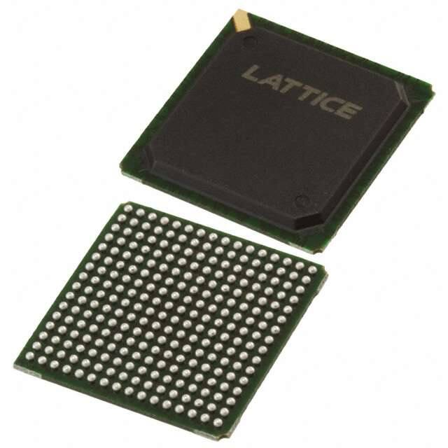


 工商网监
湘ICP备2023018690号
工商网监
湘ICP备2023018690号
