LTC4079
60V, 250mA Linear Charger
with Low Quiescent Current
Features
n
n
n
n
n
n
n
n
n
n
n
n
n
Description
Wide Input Voltage Range: 2.7V to 60V
Adjustable Battery Voltage: 1.2V to 60V
Adjustable Charge Current: 10mA to 250mA
Low Quiescent Current While Charging: IIN = 4µA
Ultralow Battery Drain When Shutdown or Charged:
IBAT < 0.01µA
Auto Recharge
Input Voltage Regulation for High Impedance Sources
Thermal Regulation Maximizes Output Current
without Overheating
Constant Voltage Feedback with ±0.5% Accuracy
NTC Thermistor Input for Temperature Qualified
Charging
Adjustable Safety Timer
Charging Status Indication
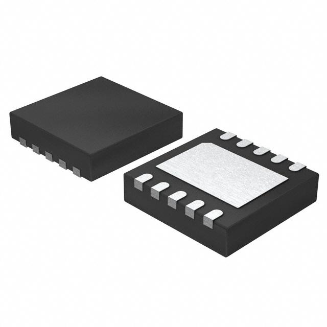
Thermally Enhanced 10-Lead (3mm × 3mm)
DFN Package
Applications
n
n
n
n
Embedded Automotive and Industrial
Backup Battery Charging from Another Battery
Energy Harvesting Charger
Thin Film Battery Products
The LTC®4079 is a low quiescent current, high voltage
linear charger for most battery chemistry types including
Li-Ion/Polymer, Lead-Acid or NiMH battery stacks up to
60V. The maximum charge current is adjustable from
10mA to 250mA with an external resistor. The battery
charge voltage is set using an external resistor divider.
With an integrated power device, current sensing and
reverse current protection, a complete charging solution
using the LTC4079 requires very few external components.
Thermal regulation ensures maximum charge current up to
the specified limit without the risk of overheating. Charging
can be terminated by either C/10 or adjustable timer.
Input voltage regulation reduces charge current when
the input voltage falls to an adjustable level or the battery
voltage, making it well suited for energy harvesting
applications. Other features include temperature qualified
charging, bad battery detection, automatic recharge with
sampled feedback in standby for negligible battery drain,
and an open-drain CHRG status output. The device is
offered in a compact, thermally enhanced 10-lead (3mm
× 3mm) DFN package.
L, LT, LTC, LTM, Linear Technology and the Linear logo are registered trademarks of Linear
Technology Corporation. All other trademarks are the property of their respective owners.
Typical Application
Li-Ion Battery Charge Cycle
Charging a Backup Battery
IN
1µF
BAT
8.4V
1.54M
LTC4079
EN
PROG NTCBIAS
10k
TIMER
NTC
GND
T 10k
+
Li-Ion
VBAT
8.4
IBAT
8.2
VBAT (V)
FBG
3.01k
120
100
FB
249k
CHRG
8.6
500mAh 2-CELL LI-ION
IBAT (mA)
9V TO 60V
140
80
8.0
60
7.8
40
C/10
7.6
TERMINATION
20
7.4
0
0
4079 TA01a
1
2
3
4
5
TIME (HOURS)
6
7
8
7.2
4079 TA01b
4079f
For more information www.linear.com/LTC4079
1
�LTC4079
Absolute Maximum Ratings
(Notes 1, 2)
IN, BAT, EN, CHRG, FB, FBG Voltage........... –0.3V to 62V
PROG TIMER Voltage...................................................3V
BAT Current....................................................... –400mA
PROG Current...................................................... –1.6mA
FBG Current..............................................................2mA
CHRG Current...........................................................2mA
Operating Junction Temperature Range
(Notes 3, 5)................................................. –40 to 125°C
Storage Temperature Range.......................–65 to 150°C
Pin Configuration
TOP VIEW
10 BAT
IN
1
EN
2
PROG
3
NTCBIAS
4
7 CHRG
NTC
5
6 TIMER
11
GND
9 FB
8 FBG
DD PACKAGE
10-LEAD (3mm × 3mm) PLASTIC DFN
TJMAX = 125°C, θJA = 43°C/W
EXPOSED PAD (PIN 11) IS GND, MUST BE SOLDERED TO PCB
Order Information
LEAD FREE FINISH
TAPE AND REEL
PART MARKING*
PACKAGE DESCRIPTION
TEMPERATURE RANGE
LTC4079EDD#PBF
LTC4079EDD#TRPBF
LGNQ
10-Lead (3mm × 3mm) Plastic DFN
–40°C to 125°C
LTC4079IDD#PBF
LTC4079IDD#TRPBF
LGNQ
10-Lead (3mm × 3mm) Plastic DFN
–40°C to 125°C
Consult LTC Marketing for parts specified with wider operating temperature ranges. *The temperature grade is identified by a label on the shipping container.
Consult LTC Marketing for information on nonstandard lead based finish parts.
For more information on lead free part marking, go to: http://www.linear.com/leadfree/
For more information on tape and reel specifications, go to: http://www.linear.com/tapeandreel/
2
4079f
For more information www.linear.com/LTC4079
�LTC4079
Electrical Characteristics
The l denotes the specifications which apply over the specified operating junction temperature range, otherwise specifications are at
TA = 25°C (Notes 2, 3). VIN = 12V, VBAT = 7.4V, VFB = 1.057V, VEN = 12V, RPROG = 3k (100mA charge current) unless otherwise specified.
SYMBOL
PARAMETER
VIN
Operating Supply Voltage
CONDITIONS
MIN
l
VBAT
Battery Voltage Range
VUVLO
VIN Undervoltage Lockout
VIN Rising
Hysteresis
l
VDUVLO
Differential Undervoltage Lockout
VIN-VBAT Rising
Hysteresis
l
VDVREG
Differential Voltage Regulation
Minimum VIN-VBAT for Charge Current
l
IQ(IN)
Input Supply Quiescent Current
Charging (Note 4)
Charging Terminated (VFB = 1.210V)
Shutdown (EN = 0)
l
l
IQ(BAT)
Battery Drain Current
Charging Terminated (VFB =1.210V)
Shutdown (EN = 0)
VIN = 0 or IN open
TYP
2.7
MAX
UNITS
60
V
60
V
2.55
140
2.7
V
mV
–20
15
80
50
mV
mV
120
160
200
mV
4
2
0.2
9
4
0.6
µA
µA
µA
0.01
0.00
0.05
0.2
0.2
0.2
µA
µA
µA
1.170
1.170
1.175
1.184
V
V
l
Charging Functions
VFB(CHG)
Feedback Pin Regulation Voltage in ConstantVoltage Charge Mode
PROG Pin Regulated Voltage
l
1.165
1.156
Constant-Current Mode
1.190
Ratio of BAT Current to PROG Pin Current
V
250
mA/mA
ICHG
Battery Charge Current in Constant-Current
Mode (Note 5)
RPROG = 1.2k
RPROG = 3k
RPROG = 30k
l
l
l
236
93
8.5
248
99
10
260
105
11.5
mA
mA
mA
ITERMINATE
Charging Termination Threshold
RPROG = 1.2k
RPROG = 3k
RPROG = 30k
l
l
l
22
8.2
0.7
25
10
1
28
11.8
1.3
mA
mA
mA
ICHG Drops Below Termination Threshold
5
9
13
ms
10
%
%
tTERMINATE
Deglitch Filter on C/10 Charge Termination
tTIMER
Safety Timer Accuracy
VRECHRG
Recharge Threshold Voltage of FB Pin
–10
Relative to VFB(CHG) with VFB Falling
VFB(LOWBAT) Low Battery Threshold
VFB for Low Battery Detection
Low Battery Time Out (Percentage of Safety
Timer)
l
Charging with VFB < VFB(LOWBAT)
96.9
97.6
98.3
0.780
0.800
0.820
V
18
%
5
Ω
RON
Resistance of the Charge Path
IFB
Feedback Pin Leakage
VFB = 1.170V (in Regulation)
VFB = 8.4V (in Shutdown)
l
l
0.1
0.1
20
100
nA
nA
IFBG
Feedback Ground Pin Leakage
VFBG = 8.4V, EN = 0
l
0.1
100
nA
RFBG
Switch Resistance from FBG Pin to GND
160
Ω
Die Temperature (TJ) at Thermal Regulation
118
°C
4079f
For more information www.linear.com/LTC4079
3
�LTC4079
Electrical Characteristics
The l denotes the specifications which apply over the specified operating junction temperature range, otherwise specifications are at
TA = 25°C (Notes 2, 3). VIN = 12V, VBAT = 7.4V, VFB = 1.057V, VEN = 12V, RPROG = 3k (100mA charge current) unless otherwise specified.
SYMBOL
PARAMETER
CONDITIONS
MIN
TYP
MAX
UNITS
%
NTC Temp Monitor
VCOLD
Low Temp. Fault NTC Threshold Voltage
VNTC/VNTCBIAS
l
72.3
73.8
75.3
VHOT
VNTC(DIS)
High Temp. Fault NTC Threshold Voltage
VNTC/VNTCBIAS
l
35.6
36.6
37.6
%
NTC Disable Voltage Threshold
VNTC
l
60
80
100
mV
Pulsed NTCBIAS Voltage
20k from NTCBIAS to Ground
NTCBIAS Period
NTCBIAS Pulse Width
NTC Input Leakage Current
VNTC = VNTCBIAS
l
4
V
3
Sec
210
µs
0.1
100
nA
Enable Input (EN)
VEN(SD)
Shutdown Threshold
VEN Falling
Hysteresis
l
0.400
0.750
55
1.100
V
mV
VEN(REG)
Enable Pin Regulation Voltage
Minimum VEN for Charge Current
l
1.170
1.190
1.210
V
l
0
20
nA
Enable Pin Leakage Current When Pulled High VEN = 60V
Status Outputs (CHRG)
Output Low Voltage
1mA Into the Open-Drain Output
l
0.16
0.4
V
Output Leakage Current
VCHRG = 60V, VEN = 0V
l
0.1
100
nA
Note 1: Stresses beyond those listed under Absolute Maximum Ratings
may cause permanent damage to the device. Exposure to any Absolute
Maximum Rating condition for extended periods may affect device
reliability and lifetime.
Note 2: Unless otherwise specified, current into a pin is positive and
current out of a pin is negative.
Note 3: The LTC4079 is tested under pulsed load conditions such that
TJ ≈ TA. The LTC4079E is guaranteed to meet performance specifications
from 0°C to 125°C junction temperature. Specifications over the –40°C
to 125°C operating junction temperature range are assured by design,
characterization and correlation with statistical process controls. The
LTC4079I is guaranteed over the full –40°C to 125°C operating junction
temperature range. Note that the maximum ambient temperature
consistent with these specifications is determined by specific operating
conditions in conjunction with board layout, the rated package thermal
impedance and other environmental factors.
4
Note 4: BAT pin charge current, PROG pin and feedback divider currents
are excluded from supply quiescent current.
Note 5: Charge current is reduced by thermal regulation as the junction
temperature rises above TLIM (118°C).
4079f
For more information www.linear.com/LTC4079
�LTC4079
Typical Performance Characteristics
Regulated Feedback Voltage
vs Temperature
Load Regulation of Regulated
Feedback Voltage
Regulated Feedback Voltage
vs VIN
1.182
1.182
1.178
1.178
1.178
1.174
1.174
VFB(CHG) (V)
INTERNAL REFERENCE
1.170
ONSET OF
THERMAL REGULATION
1.166
1.162
VFB(CHG) (V)
1.182
1.174
VFB(CHG) (V)
VIN = 12V, TA = 25°C unless otherwise noted.
1.170
1.166
1.162
1.158
–50 –25
0
25 50 75 100 125 150
TEMPERATURE (°C)
1.158
0
10
20
30
VIN (V)
50
40
5
1.158
0.15
VFB = 1.2V
(IBAT = 0)
3
IBAT (µA)
IIN (µA)
2
STANDBY
(CHARGING TERMINATED)
2
200
250
Battery Quiescent Current
vs Temperature
0.20
4
CHARGING
STANDBY
(CHARGING TERMINATED)
100
150
IBAT (mA)
50
0
4079 G03
CHARGING
4
IIN (µA)
60
Input Supply Quiescent Current
vs Supply Voltage
VFB = 1.2V
(IBAT = 0)
3
1.166
4079 G02
Input Supply Quiescent Current
vs Temperature
5
1.170
1.162
4079 G01
6
RPROG = 1.2k
ICHG = 248mA
VBAT = 8.4V
CHARGING TERMINATED
OR SHUTDOWN
0.10
0.05
1
1
SHUTDOWN (EN = 0)
SHUTDOWN (EN = 0)
0
–50 –25
0
0
25 50 75 100 125 150
TEMPERATURE (°C)
0
10
20
30
VIN (V)
50
40
4079 G04
60
120
50
SHUTDOWN (EN = 0)
40
30
VBAT (V)
50
60
4079 G07
0
ONSET OF THERMAL
REGULATION
VIN = 12V
VBAT = 8.4V
RPROG = 1.2k
200
IBAT (mA)
IBAT (nA)
IBAT (mA)
20
20
250
RPROG = 3k
60
10
10
300
80
40
0
Battery Charge Current
vs Temperature
VFB(CHG) = 8.4V
100
STANDBY
(CHARGING TERMINATED)
20
0
25 50 75 100 125 150
TEMPERATURE (°C)
4079 G06
Battery Charge Current
vs Battery Voltage
30
0
4079 G05
Battery Quiescent Current
vs Battery Voltage
40
0
–50 –25
60
150
100
50
RPROG = 30k
0
2
4
6
VBAT (V)
RPROG = 3k
RPROG = 30k
8
10
4079 G08
0
–50 –25
0
25 50 75 100 125 150
TEMPERATURE (°C)
4079 G09
4079f
For more information www.linear.com/LTC4079
5
�LTC4079
Typical Performance Characteristics
Battery Charge Current
vs VIN – VBAT
Battery Charge Current vs VEN
RPROG = 3k
100
RPROG = 3k
100
60
40
OHMIC REGION
(DROPOUT)
60
40
20
20
RPROG = 30k
0
1.18
1.19
1.12
VEN (V)
1.21
RPROG = 30k
0
0.0
1.22
0.1
0.2
0.3
0.4
VIN – VBAT (V)
10
0
6
4
0
25 50 75 100 125 150
TEMPERATURE (°C)
0
20
10
30
VIN (V)
40
4079 G13
350
50
0
25 50 75 100 125 150
TEMPERATURE (°C)
4079 G16
6
10
PIN AT 1.2V
5
0
25 50 75 100 125 150
TEMPERATURE (°C)
4079 G15
NTCBIAS Period and Pulse Width
vs Temperature
3.2
260
3.1
250
3.0
240
1.1
PERIOD (s)
TIMER DURATION (RELATIVE TO 25°C)
RFBG (Ω)
100
250
1.0
2.9
230
PERIOD
2.8
0.9
220
PULSE WIDTH
2.7
0.8
–50 –25
PULSE WIDTH (µs)
150
200
PIN AT 60V
0
–50 –25
60
1.2
200
0
–50 –25
50
15
Normalized Timer Duration
vs Temperature
250
100
150
IBAT (mA)
4079 G14
Switch Resistance from
FBG to GND vs Temperature
300
50
20
2
VIN = 5.0V
0
–50 –25
0
EN and FB Pin Leakages
vs Temperature
LEAKAGE CURRENT (nA)
RON (Ω)
RON (Ω)
5
230
4079 G12
PULSED LOAD (TJ ≈TA)
VIN – VBAT = 0.6V
RPROG = 1.2k
8
VIN = 2.7V
240
210
0.6
THERMAL REGULATION
10
250
Charge Path Dropout Resistance
vs VIN
PULSED LOAD (TJ ≈TA)
VIN – VBAT = 0.6V
RPROG = 1.2k
15
260
4079 G11
Charge Path Dropout Resistance
vs Temperature
20
270
220
0.5
4079 G10
4 DEVICES TESTED
RPROG = 1.2k
280
80
IBAT (mA)
80
IBAT (mA)
IBAT/IPROG Ratio vs IBAT
290
120
IBAT/ I PROG (mA/mA)
120
25
VIN = 12V, TA = 25°C unless otherwise noted.
0
25 50 75 100 125 150
TEMPERATURE (°C)
4079 G17
2.6
–50 –25
210
0
200
25 50 75 100 125 150
TEMPERATURE (°C)
4079 G18
4079f
For more information www.linear.com/LTC4079
�LTC4079
Pin Functions
IN (Pin 1): Input Supply Pin. This input provides power
to the battery charger. Bypass this pin with a ceramic
capacitor of at least 1µF.
EN (Pin 2): Enable Input. Charge current starts flowing
when this input rises above 1.190V, its regulation threshold.
When using a current limited power source, connect this
input to an external resistor divider from IN to GND to avoid
UVLO oscillations. This configuration can also be used
to maintain the source voltage (IN pin) at the maximum
power threshold (e.g., for solar panel). Pulling this pin
below 0.750V shuts down the device. This pin should
not be left floating.
PROG (Pin 3): Charge Current Program Pin. The current
out of this pin is 1/250th of the current out of the BAT
pin. A resistor connected from PROG to ground sets the
charge current in constant-current mode. This pin servos
to 1.190V during constant-current charging. Do not leave
this pin open. Limit parasitic capacitance on this node to
less than 50pF.
NTCBIAS (Pin 4): NTC Thermistor Bias Output. Connect
a low drift bias resistor from NTCBIAS to NTC pin, and
a thermistor from NTC pin to GND. The value of the bias
resistor is typically equal to the nominal resistance of
the thermistor at 25°C. Minimize parasitic capacitance
on this pin.
NTC (Pin 5): Input to the Battery Temperature Sense
Circuit. Connect the NTC pin to a negative temperature
coefficient (NTC) thermistor, which is typically co-packaged
with the battery, to signal the charger if the battery is too
hot or too cold to charge. The room temperature value
of the thermistor should be at least 2kΩ. If the battery’s
temperature is out of range, charging is paused until the
battery temperature re-enters the valid range. Connect a
1%, low drift bias resistor from NTCBIAS to NTC and a
thermistor from NTC to ground. Minimize parasitic capacitance on this pin. Tie the NTC pin to GND to disable
battery temperature sensing.
For maximum charge duration of tTIMER (in Hours), the
required capacitance value can be determined as follows:
CTIMER = (tTIMER • 18.2nF/Hr)
A typical value of CTIMER is 100nF which terminates the
charge cycle after 5½ hours. Minimize leakage on this pin
to maintain timer accuracy.
The timer is disabled when this pin is tied to GND. In this
case charging terminates when the charge current falls
below 1/10th of the programmed charge current ICHG.
CHRG (Pin 7): Open-Drain Charge Status Output. Typically
pulled up to a voltage source through a resistor or a low
power LED and a resistor. This pin is pulled low by an
internal NMOS when LTC4079 is charging the battery.
The pin goes to high impedance when the charge current
drops below 1/10th of the programmed current, or the
charge cycle is timer terminated.
FBG (Pin 8): Ground Reference for Battery Voltage Divider.
This pin is connected to ground internally through an NMOS
switch when the battery is charging and disconnects the
battery voltage divider from GND when it is not needed.
When sensing the battery voltage the NMOS switch
presents a low resistance (RFBG =160Ω) to GND.
FB (Pin 9): Sense Pin for Divided Battery Voltage. This pin
servos to 1.170V (VFB(CHG)) during the constant-voltage
phase of the battery charge algorithm. The battery charge
voltage is set by using an appropriate resistor divider
from BAT to FB to FBG. Minimize leakage and parasitic
capacitance on this pin.
BAT (Pin 10): Battery Charger Output. This pin provides
charge current to the battery.
GND (Exposed Pad Pin 11): Ground. The exposed pad
must be soldered to a continuous ground plane of the
printed circuit board for electrical connection and the rated
thermal performance.
TIMER (Pin 6): Timer Capacitor Input. A capacitor on this
pin sets the maximum duration for battery charging from
charger enable or from the beginning of a recharge cycle.
4079f
For more information www.linear.com/LTC4079
7
�LTC4079
Block Diagram
1
IN
BAT
P1
IBAT
250
CC/CV REGULATION,
EN REGULATION,
VIN-VBAT REGULATION
THERMAL REGULATION
BG REF
10
RFB1
FB
+
9
T
–
BATTERY PACK
+
2
7
EN
RECHARGE
REFERENCE
FBG
RFB2
8
UVLO,
DIFF UVLO
CHRG
NTCBIAS
CONTROL
4
RBIAS
NTC
5
OSC
PROG
TIMER
6
3
CTIMER
4079 F01
RPROG
Figure 1. Block Diagram of LTC4079
8
4079f
For more information www.linear.com/LTC4079
�LTC4079
Operation
The LTC4079 is a full featured constant-current, constantvoltage charger designed to charge multiple chemistry
types of batteries from voltage sources up to 60V. The low
quiescent current of the device minimizes power drain on
the source and the battery, making it suitable for a variety
of applications including backup and energy harvesting
from an intermittent power source. The battery charge
voltage is set using an external resistor divider. Charge
duration can be set using a capacitor on the TIMER pin.
For safety and improved battery life, the LTC4079 includes
a thermistor input for temperature qualified charging.
A 6ms filter (tTERMINATE) is used on the C/10 detector to
prevent premature termination due to transient loads on
the battery during charging.
Charge current starts when the EN pin is brought above
1.190V. Figure 2 shows a flow chart of the primary states
and state transitions of the LTC4079. A typical charge
cycle includes:
The battery charge voltage is set by connecting a resistor
divider from the battery to the FB and FBG pins as shown
in Figure 3. The charge voltage is determined as follows:
1. Constant-Current (CC) Charging: The programmed
charge current is used to charge the battery until the
battery voltage reaches the charge voltage set using
the feedback divider. For a low ESR battery, this mode
provides the bulk of the charge. The charge timer should
generally be set long enough to charge the battery above
the recharge threshold, otherwise another charge cycle
would immediately follow.
4. Automatic Recharge: When VBAT drops below the
recharge threshold (97.6% of the charge voltage),
whether by battery drainage or replacement of the
battery, the charger automatically re-engages and starts
charging.
Setting The Battery Charge Voltage
where RFB1 is the resistor from BAT to FB, RFB2 is the
resistor from FB to FBG and RFBG is the resistance of the
internal switch of the FBG pin (160Ω typical).
BAT
RFB1
LTC4079
2. Constant-Voltage (CV) Charging: Once the battery
reaches the set charge voltage, constant voltage is
maintained across the battery by controlling the charge
current. The charge current reduces with time in this mode
as the battery nears its full charge capacity.
3. Charging Termination: The LTC4079 can be configured
to terminate charging automatically based on time or
current. The CHRG status pin goes to high impedance
when the charge current reduces below 1/10th of the
programmed current, indicating that the battery is almost
fully charged. The charge current continues to top-off the
battery until the timer terminates the charge current. Timer
termination can be disabled by connecting the TIMER
pin to ground. In this case, charging terminates when
the charge current falls below 1/10th of the programmed
charge current.
RFB1
VCHG = 1.170V • 1+
RFB2 +RFBG
FB
FBG
RFB2
+
BATTERY
4079 F03
ENABLE
Figure 3. Setting the Battery Charge Voltage
Setting and Monitoring the Charge Current
The charge current delivered to the battery in constantcurrent mode, ICHG is set using a resistor from the PROG
pin to ground. The value of this resistor is calculated using:
RPROG =
297.5V
ICHG
4079f
For more information www.linear.com/LTC4079
9
�LTC4079
Operation
SHUTDOWN*
VEN > 0.805V
VIN > 2.57V
VIN – VBAT > 15mV?
NO
YES
ASSERT CHRG STATUS
START SAFELY TIMER IF
TIMER NOT GROUNDED
BATTERY TEMP
IN RANGE?
NO
PAUSE CHARGE CURRENT
PAUSE TIMER
YES
EN REG, DIFF REG
OR THERMAL REG
NO CV REG?
YES
NO
YES
BAD BATTERY*
CHRG REMAINS
ASSERTED
YES
RUN TIMER
PAUSE TIMER
CC-CV CHARGING
CHARGING IN EN REG,
DIFF REG OR THERMAL REG
LATCH-OFF*
CHRG REMAINS
ASSERTED
VFB < 0.8V?
NO
YES
SAFETY TIMER
EXPIRED?
1/4 SAFETY TIMER
EXPIRED?
NO
YES
NO
NO
VFB < VRECHG?
YES
RETRY COUNT = 5?
NO
INCREMENT
RETRY
COUNTER
NO
ICHG < C/10?
IN CV REG, NO EN REG,
DIFF REG OR
THERM REG
STANDBY
CHARGING TERMINATED
RESET SAFETY TIMER
RESET RETRY COUNTER
DEASSERT CHRG STATUS
SAMPLE FB PIN EVERY 3 SEC
YES
VFB < VRECHG
4079 F02
DEASSERT CHRG SATUS
TIMER
GROUNDED?
YES
NO
* VEN < 0.75V OR ULVO TAKES THE DEVICE
TO SHUTDOWN FROM ANY STATE
Figure 2. Battery Charger Operations Flow Chart
10
4079f
For more information www.linear.com/LTC4079
�LTC4079
Operation
The PROG pin also provides a voltage signal proportional
to the battery charge current. Therefore, the instantaneous
battery current can be determined as follows by monitoring
the PROG pin voltage:
IBAT =
250 • VPROG
RPROG
Minimize the parasitic capacitance while monitoring the
PROG pin voltage as any capacitance on this pin forms a
pole that may cause instability in the charge control loop.
LTC4079
NTC SAMPLE
PULSE
BAT
NTCBIAS
INTERNAL SUPPLY
NTC
TOO COLD
+
–
TOO HOT
+
–
36.6% VNTCBIAS
IGNORE NTC
+
–
0.1V
Undervoltage Detection
RBIAS
73.8% VNTCBIAS
RNTC
T
+
4079 F04
An internal undervoltage lockout circuit monitors the VIN
voltage and disables the battery charging circuit until VIN
rises above the undervoltage lockout threshold, 2.55V
(typically). The UVLO threshold has built-in hysteresis
of 140mV. Furthermore, the differential UVLO circuit
also keeps the charger in a low quiescent current mode
by disabling the battery charging circuits when VIN falls
below VBAT by more than 65mV. The differential UVLO
has hysteresis of 80mV, with turn-on at VIN-VBAT = 15mV
(typical).
Battery Temperature Qualified Charging
During battery charging, the battery temperature is sensed
by sampling the voltage on the NTC pin every 3 seconds.
Connect a low drift bias resistor from the NTCBIAS output
to the NTC input and a negative temperature coefficient
(NTC) thermistor, close to the battery pack, from the NTC
pin to ground, as shown in Figure 4. The bias resistor should
be equal to the value of the chosen thermistor at 25°C.
The LTC4079 pauses charging and the charge timer when
the NTC pin voltage indicates that the thermistor resistance
has dropped to 0.576 times its room temperature value.
For a Vishay curve 2 thermistor, this corresponds to 40°C.
Charging is also paused when the thermistor resistance
increases to 2.816 times the room temperature value. For
a Vishay curve 2 thermistor, this increase corresponds
to 0°C.
The hot and cold trip points can be adjusted using a
different type of thermistor, or a different RBIAS resistor,
or by adding a desensitizing resistor in series with the
thermistor, or by a combination of these measures.
Figure 4. Battery Temperature Sensing Using NTC Thermistor
Charging resumes when the battery temperature returns to
the normal range and the timer continues from the point
where it was paused.
Input Voltage Regulation
The LTC4079 can regulate a constant voltage on the IN pin
when charging from a current-limited power source such
as a weak battery or a solar panel. This feature can be used
to prevent the input voltage from collapsing below UVLO,
or to maintain the input source voltage at peak power.
The charge current is reduced as the input voltage falls to
the threshold set by an external resistor divider from the
input power source to the EN pin and GND, as shown in
Figure 5. The input voltage regulation threshold, VIN(REG)
is calculated as follows:
R
VIN(REG) = 1.190V • 1+ EN1
REN2
This regulation mechanism allows the charge current to be
selected based on battery requirement and the maximum
power available from the charging source. The LTC4079
automatically reduces the charge current when the input
source cannot provide the programmed charge current.
When input voltage regulation is not needed, connect the
EN pin to the input power source or a digital enable signal.
For more information www.linear.com/LTC4079
4079f
11
�LTC4079
Operation
INPUT POWER
SOURCE
IN
REN1
LTC4079
EN
REN2
4079 F05
Figure 5. Setting Input Voltage Regulation
Differential Voltage (VIN-VBAT) Regulation
The LTC4079 provides an additional method to keep the
input voltage from collapsing when the input power comes
from a weak power source. If the input voltage falls close
to the battery voltage, the differential voltage regulation
loop in LTC4079 keeps the input voltage above the battery
voltage by 160mV (typical value) by reducing the charge
current as the input to battery differential voltage falls.
When C/10 termination is used, the LTC4079 provides
battery charge current as long as the current remains
above the C/10 threshold. As the battery terminal voltage
reaches the target charge voltage, the charge current falls
until the C/10 threshold is reached, at which time the
charger terminates and the LTC4079 enters standby mode.
Premature termination is prevented when input voltage,
differential or thermal regulation is active.
To prevent termination-recharge oscillations, it is important
to set the termination charge current low enough for batteries with high internal resistance. For a nominal recharge
threshold of 2.4% below the charge voltage, the charge
current should be set as follows with sufficient margin:
V
ICHG < 0.24 • CHG
RBAT
In both of the above regulation conditions, the input source
must provide at least the quiescent current of the device to
prevent UVLO. The charge timer is paused whenever the
charge current is reduced due to input voltage regulation
or differential voltage regulation.
where RBAT is the battery's internal series resistance. The
CHRG status pin is high impedance when the charger is
not actively charging.
Thermal Regulation
The LTC4079 also supports a timer-based termination
scheme, where the battery charge cycle is terminated after
a specific amount of time elapses. Connect a capacitor
from the TIMER pin to ground to engage timer based
charge termination. Calculate the capacitance required
for the desired charge cycle duration, tTIMER as follows:
An internal thermal feedback loop reduces the charge
current below the programmed value if the die temperature
approaches 118°C. This feature protects the LTC4079
from excessive temperature and allows the user to set
the charge current to typical (not worst case) ambient
temperature with the assurance that the charger will
automatically reduce the current to prevent overheating
in worst-case conditions.
The charge timer is paused during thermal limiting to
prevent under-charging the battery and to allow the full
charge current to flow for the set timer duration.
C/10 Termination
The LTC4079 supports a current based termination scheme,
where a battery charge cycle terminates when the current
output from the charger falls below one-tenth of the
programmed charge current. The C/10 threshold current
corresponds to 119mV on the PROG pin. This termination
mode is engaged by shorting the TIMER pin to ground.
12
Timer Termination
CTIMER = tTIMER • 18.2nF/Hr
A 200nA current source is used to source/sink current
to/from CTIMER to generate a sawtooth periodic signal
(nominally 0.8V to 1.2V) for use by the timer. Since the
TIMER pin current is small, minimize leakage on this pin
to maintain timer accuracy.
The timer starts on charger enable or the beginning of a
recharge cycle, and is reset on disable or when VIN falls
below UVLO or DUVLO.
The timer is paused whenever the charge current is limited
by EN pin or differential voltage or thermal regulation,
unless the charger is also in constant-voltage regulation
mode. It is also paused with the charge current during an
NTC fault. The timer is not paused if the charge current is
4079f
For more information www.linear.com/LTC4079
�LTC4079
Operation
limited by dropout. For example, for a programmed charge
current of 100mA, this occurs when VIN-VBAT falls below
about 0.5V due to the voltage drop across the charge path
(5Ω typically). If VIN-VBAT falls below 160mV to trigger
differential voltage regulation, the timer will be paused.
The CHRG status pin signals charging at a rate of more
than C/10, regardless of which termination scheme is
used. When timer termination is used, the CHRG status
pin pulls low during a charging cycle until the charger
output current falls below the C/10 threshold. The charger
continues to top off the battery until timer termination,
when the LTC4079 enters standby mode.
Standby and Automatic Recharge
If the LTC4079 remains enabled after charge cycle
termination, it monitors the battery voltage in standby
mode by sampling the FB pin connected to the external
resistor divider. In order to minimize the battery drain, the
feedback divider is only turned on (by connecting FBG pin
to ground) for 210µs once every 3 seconds. When this
sampling detects that the battery voltage has dropped
by more than 2.4%, the feedback divider is kept on for
1.5 seconds (typical). If the FB voltage remains below
the recharge threshold for more than 2.5ms (typical), a
recharge cycle starts. This 2.5ms filter prevents premature
recharge due to load transients. The recharge cycle also
terminates in constant-voltage charge mode as described
above. The automatic recharge function maintains that the
battery at, or near, a fully charged condition.
If the battery voltage remains below the recharge threshold
on timer expiration, another recharge cycle begins as
explained below.
Timer Retry and Latch-off
A new charge cycle is started if the battery voltage remains
below the recharge threshold at the end of a charge cycle.
This happens in the following situations: 1) the timer is
not set long enough for the battery with the programmed
charge current, 2) the battery is defective, 3) a load drains
the battery during charging, 4) charge current is limited
by dropout.
In order to avoid wasting power in recharging a defective
battery indefinitely, LTC4079 contains a recharge latchoff feature. Charging is latched off and the CHRG pin
remains asserted after 5 recharge attempts if the battery
voltage remains below the recharge threshold at the end
of all five recharge cycles. The latch-off counter is reset
if a charge cycle terminates normally during any recharge
attempt, or if the charge current falls below ICHG/10 in
constant-voltage regulation mode during a charge cycle.
Charger disable using the EN pin or UVLO also resets the
latch-off counter..
Bad Battery Scenario
If the feedback voltage remains below VFB(LOWBAT) for
longer than 1/4th of the safety timer set by CTIMER, the
battery is considered bad. Charging stops in this case and
the CHRG pin remains asserted. NTC sampling and FB
sampling for recharge is also turned-off. The charge cycle
is restarted by toggling the EN pin below VEN(SD) (typically
0.75V) and then back high. UVLO also clears the bad battery
lockout. There is no bad battery detection when the battery
charge timer is disabled (TIMER pin grounded).
CHRG Status Output
The charge status open-drain output (CHRG) has two
states: pull down and high impedance. The pull-down
state indicates that LTC4079 is in charging mode. A high
impedance state indicates that the charge current has
dropped below 10% of the programmed charge current. In
most cases, charge current is reduced due to the constantvoltage loop, meaning that the battery voltage is near the
target charge voltage. But if charge current is reduced due
to VIN regulation (through EN or VIN-VBAT regulation) or
thermal regulation, CHRG remains asserted until only the
constant-voltage regulation loop reduces charge current
below 10% of the programmed charge current.
A high impedance state at the CHRG pin occurs on timer
termination, or UVLO or differential UVLO, or when the
LTC4079 is disabled by pulling EN low. This output can
be used as a logic interface or to light a low power LED.
4079f
For more information www.linear.com/LTC4079
13
�LTC4079
Applications Information
Feedback Divider Selection
Using too low or too high values of resistors for the
feedback divider can cause small charge voltage errors
due to: 1) Finite on-resistance of the internal switch on
the FBG pin and 2) leakage on the FB pin. The impact of
these two factors on the target battery charge voltage is
calculated as follows:
RFB1
VCHG = 1.170V • 1+
+RFB1 •(IFB +ILEAK )
RFB2 +RFBG
where RFB1 and RFB2 are the top and bottom resistors of
the feedback divider, RFBG is the resistance of the internal
switch from the FBG pin to GND (160Ω typical) and ILEAK
is the parasitic leakage on the FB pin as shown in Figure
6. A graph of IFB vs Temperature is given in the Typical
Performance section.
According to the above equation, high value feedback
resistors minimize the impact of RFBG, while low values
minimize the impact of IFB and lLEAK. A Thevenin equivalent
resistance of 100k to 500k on the FB node is generally a
good compromise in most scenarios.
BAT
LTC4079
IFB
ENABLE
FB
FBG
+
RFB1
RFB2
ILEAK
BATTERY
4079 F06
PARASITIC
LOAD
VCHG
RFB1
RFB2
TYPICAL ERROR
3.6V
1070k
511k
+0.53%
4.1V
422k
169k
–0.27%
4.2V
1070k
412k
+0.18%
7.2V
1370k
267k
–0.42%
8.2V
1070k
178k
-0.04%
8.4V
1540k
249k
+0.02%
12.3V
1780k
187k
-0.02%
12.6V
2550k
261k
-0.05%
Stability Considerations
When the charger is in constant-current mode, the PROG
pin impedance forms part of the charger current control
loop. The constant-current mode stability is therefore
affected by the roll-off frequency of the PROG pin
impedance. With minimum capacitance on this pin (less
than about 10pF), the charger is stable with a program
resistor, RPROG, as high as 60k (ICHG = 5mA); however,
any additional capacitance at this pin limits the maximum
allowed program resistor.
The constant-voltage loop is stable without any
compensation as long as a typical low impedance battery
is connected to the BAT pin. However, a 1µF capacitor with
1Ω series resistor is recommended when charging high
ESR batteries, typically more than 1kΩ.
Charging High Resistance Batteries
Figure 6. Feedback Divider Considerations
For example, for RFB1 = 1.54M and RFB2 = 249k (for battery charge voltage of 8.4V), accounting for RFBG =160Ω
lowers the charge voltage by 0.06%, while ILEAK = 10nA
raises it by 0.18%.
Table 1 lists possible choices of standard 1% resistor
values for common battery charge voltages. The Typical
Error column gives systematic error due to the granularity
in the values of 1% resistors.
14
Table 1. Recommended 1% Resistors for Common Battery
Charge Voltages
When charging a battery with high internal resistance,
the battery voltage can rise quickly, entering constantvoltage mode. If the charge current falls below 1/10th of
the programmed charge current, charging may terminate
based on C/10 even if a timer capacitor is connected
on the TIMER pin. This is because C/10 termination is
assumed if the timer pin remains below 0.3V. With only
200nA being sourced from the TIMER pin, a large timer
capacitance may limit the TIMER voltage below 0.3V for
a short duration at the beginning of a charge cycle. After
charging terminates, a recharge cycle would begin if the
4079f
For more information www.linear.com/LTC4079
�LTC4079
Applications Information
internal battery voltage has not been charged above the
recharge threshold, determined by ∆VRECHRG and the
feedback divider. As shown in Figure 7, this charge/recharge
cycle continues until the TIMER pin rises above 0.3V, at
which point timer termination is engaged and the battery
is charged for the duration set by the timer capacitor.
4.2V
VBAT
0.2V/DIV
PROG
0.1V/DIV
TA = 118°C – (12V-6.6V) • 100mA • 43°C/W = 95°C
Increasing Thermal Regulation Current
CHRG
5V/DIV
20ms/DIV
4079 F01
Figure 7. Repeated Charge Terminations on
Startup Due to High Resistance of the Battery,
CTIMER = 82nF, VCHG = 4.2V, ICHG = 10mA and
Battery Resistance = 300Ω
Power Dissipation and Thermal Regulation
The LTC4079 automatically reduces charge current
during high power conditions that result in high junction
temperature. Therefore, it is not necessary to design
the charging system for worst-case power dissipation
scenarios. The conditions that cause the LTC4079 to
reduce charge current through thermal regulation can be
approximated by considering the power dissipated in the
IC. Most of the power dissipation is in the charge path.
Thus the power dissipation is approximately:
PD = (VIN-VBAT) • IBAT
The approximate ambient temperature at which the thermal
regulation begins to lower the charge current is:
TA = 118°C – PD • θJA
TA = 118°C – (VIN-VBAT) • IBAT • θJA
The reduced charge current at an ambient temperature
above the onset of thermal regulation can be calculated
as follows:
Assuming θJA is 43°C/W the ambient temperature at which
the charge current begins to fall due to thermal regulation is:
The LTC4079 can be used above 95°C ambient but the
charge current will be reduce linearly from the programmed
value of 100mA to 0mA as the ambient temperature
increases from 95°C to 118°C.
TIMER
0.5V/DIV
IBAT =
Example: Consider an LTC4079 operating from a 12V
input source programmed to supply 100mA current to
a discharged 2-cell Li-Ion battery with a voltage of 6.6V.
In applications with large VIN to VBAT drop, the charge
current can be significantly reduced during thermal regulation. One way to increase the thermally regulated charge
current is to dissipate some of the power in a resistor in
series with the IN pin. This works well when the resistor
value is designed to be small enough to avoid pushing the
LTC4079 into dropout.
Input Capacitor Selection
When an input supply is connected to a portable product,
the inductance of the cable and the high Q ceramic input
capacitor form an L-C resonant circuit. While the LTC4079
is capable of withstanding input voltages as high as 62V, if
the input cable does not have adequate mutual inductance
or if there is not much impedance in the cable, it is possible
for the voltage at the input of LTC4079 to reach as high as
2x the cable input voltage before it settles out. To prevent
excessive voltage from damaging the LTC4079 during a
hot insertion, it is best to have a low voltage coefficient
capacitor at the supply input pin of the LTC4079.
Using a tantalum capacitor or an aluminum electrolytic
capacitor for input bypassing, or paralleling with a ceramic capacitor will also reduce voltage overshoot during
a hot insertion.
118°C – TA
( VIN – VBAT ) • θJA
4079f
For more information www.linear.com/LTC4079
15
�LTC4079
Applications Information
Board Layout Considerations
When laying out the printed circuit board, the following
checklist should be followed to ensure proper operation
of the LTC4079:
1. Connect the exposed pad of the package (Pin 11)
directly to a large PC board ground to minimize thermal
impedance. Correctly soldered to a 1500mm2 double
sided 1oz copper board, the LTC4079 DFN package has
a thermal resistance (θJA) of approximately 43°C/W.
Failure to make good contact between the exposed pad
on the backside of the package and an adequately sized
ground plane results in much larger thermal resistance.
3. Minimize the parasitic capacitance and leakage on the
FB node for stability and charge voltage accuracy.
4. Minimize the parasitic capacitance and leakage on the
TIMER pin for timer accuracy.
5. Minimize the parasitic capacitance on the PROG pin for
stable operation.
6. Minimize the parasitic capacitance and leakage on the
EN pin if it is connected to a resistor divider from the
input supply for input voltage regulation.
2. The top of the feedback divider resistor should be
connected as close to the positive battery terminal as
possible in order to avoid inaccuracies due to voltage
drop in the charge current path. The negative terminal
of the battery should be connected to the chip ground
plane directly to avoid any ground loop induced charge
voltage inaccuracy.
16
4079f
For more information www.linear.com/LTC4079
�LTC4079
Typical Applications
Li-Ion Charger with Timer Termination
In the Figure 8 configuration, the input source charges
the battery for 5½ hours and also supplies current to the
load. The maximum current provided by the charger (on
BAT pin) is limited to the charge current of 246mA set by
the 1.21k resistor on the PROG pin. A small resistor is
used in series with the input supply to reduce VIN-VBAT,
and thereby increase the available charge current during
thermal regulation. Once the battery is charged, it supplies power to the load until VBAT falls below the recharge
threshold, at which point a recharge cycle starts.
Li-Ion Charging from a Solar Panel with Differential
Voltage Regulation, C/10 Termination
Figure 10 shows a simple charging solution from a solar
panel. Differential voltage regulation reduces charge current
to prevent the panel voltage from drooping below the
battery voltage when charging under low light conditions.
The LTC4079 does not require a Schottky diode in series
with the panel.
IN
1µF
24V
SUPPLY
25Ω, 2W
IN
BAT
LTC4079
EN
1µF
1.54M
–
249k
CHRG
FBG
NTCBIAS
CHRG
FBG
PROG
NTCBIAS
TIMER
NTC
TIMER
100nF
NTC
GND
T
VCHG = 8.4V
ICHG = 246mA
10k
1.21k
VCHG = 8.4V
ICHG = 246mA
GND
T
+
BATTERY
PACK
10k
+
BATTERY
PACK
10k
TO
LOAD
FB
10k
1.21k
1µF
1.54M
249k
SOLAR
PANEL
FB
PROG
EN
+
TO
LOAD
BAT
LTC4079
4079 F10
Figure 10. Li-Ion Charger with Differential Voltage Regulation
4079 F08
Figure 8. Li-Ion Charger with Timer Termination
Supercapacitor Charger from 2-Cell Li-ion
2-Cell NiMH Trickle Charger from Automotive Supply
with Timer Termination
Figure 9 shows a trickle charger for 2-cell, 2500mAh,
AA NiMH battery with timer termination after 31 hours.
Charge current drops when the battery voltage reaches
1.65V per cell.
12V
CAR BATTERY
IN
BAT
LTC4079
EN
1µF
324k
2-CELL
Li-Ion
IN
+
CHRG
FBG
EN
VCHG = 3.3V
ICHG = 99mA
PROG
NTCBIAS
TIMER
NTC
3.01k
+
2500mAh
2-CELL
NiMH
4079 F09
TO
LOAD
BAT
LTC4079
FB
178k
560nF
TO
LOAD
Charging terminates when the stacked supercapacitor
voltage reaches the set charge voltage. A recharge cycle
begins automatically when the supercap voltage falls
below the recharge threshold. A resistor divider balancer
can optionally be switched in for balancing a stacked
supercapacitor during charging.
1.02M
VCHG = 5.0V
ICHG = 10mA
FB
309k
CHRG
FBG
PROG
NTCBIAS
TIMER
NTC
30.1k
1k
FDG6308P
CSC
0.6F
HS206
1k
GND
GND
SUPERCAP BALANCER (OPTIONAL)
4079 F11
Figure 9. NiMH Trickle Charger with Timer Termination
Figure 11. Supercap Charger with C/10 Termination
4079f
For more information www.linear.com/LTC4079
17
�LTC4079
Typical Applications
12V Lead-Acid Charger from Rectified 24V AC
In the following charging circuit example, a lead acid
battery is trickle charged at a C/10 rate for 15 hours. An
NTC thermistor is used to alter the target charge voltage
of the lead-acid battery based on the battery temperature.
IN
100µF
BAT
LTC4079
ICHG = 99mA
+
1M
EN
100k
CHRG
FB
102k
24V AC
T
1µF
TO
LOAD
12V
LEAD-ACID
BATTERY
100k
FBG
PROG
NTCBIAS
3.01k
NTC
TIMER
270nF
GND
4079 F12
Figure 12. Lead-Acid Battery Trickle Charger from Rectified 24V AC
18
4079f
For more information www.linear.com/LTC4079
�LTC4079
Package Description
Please refer to http://www.linear.com/designtools/packaging/ for the most recent package drawings.
DD Package
10-Lead Plastic DFN (3mm × 3mm)
(Reference LTC DWG # 05-08-1699 Rev C)
0.70 ±0.05
3.55 ±0.05
1.65 ±0.05
2.15 ±0.05 (2 SIDES)
PACKAGE
OUTLINE
0.25 ± 0.05
0.50
BSC
2.38 ±0.05
(2 SIDES)
RECOMMENDED SOLDER PAD PITCH AND DIMENSIONS
3.00 ±0.10
(4 SIDES)
R = 0.125
TYP
6
0.40 ± 0.10
10
1.65 ± 0.10
(2 SIDES)
PIN 1 NOTCH
R = 0.20 OR
0.35 × 45°
CHAMFER
PIN 1
TOP MARK
(SEE NOTE 6)
0.200 REF
0.75 ±0.05
0.00 – 0.05
5
1
(DD) DFN REV C 0310
0.25 ± 0.05
0.50 BSC
2.38 ±0.10
(2 SIDES)
BOTTOM VIEW—EXPOSED PAD
NOTE:
1. DRAWING TO BE MADE A JEDEC PACKAGE OUTLINE M0-229 VARIATION OF (WEED-2).
CHECK THE LTC WEBSITE DATA SHEET FOR CURRENT STATUS OF VARIATION ASSIGNMENT
2. DRAWING NOT TO SCALE
3. ALL DIMENSIONS ARE IN MILLIMETERS
4. DIMENSIONS OF EXPOSED PAD ON BOTTOM OF PACKAGE DO NOT INCLUDE
MOLD FLASH. MOLD FLASH, IF PRESENT, SHALL NOT EXCEED 0.15mm ON ANY SIDE
5. EXPOSED PAD SHALL BE SOLDER PLATED
6. SHADED AREA IS ONLY A REFERENCE FOR PIN 1 LOCATION ON THE
TOP AND BOTTOM OF PACKAGE
4079f
Information furnished by Linear Technology Corporation is believed to be accurate and reliable.
However, no responsibility is assumed for its use. Linear Technology Corporation makes no representation that the interconnection
of its circuits
as described
herein will not infringe on existing patent rights.
For more
information
www.linear.com/LTC4079
19
�LTC4079
Typical Application
Energy Harvesting Charger with Buck, Buck-Boost and LDO Supplies
4V TO 19V
3V TO 19V
+
1µF
6.3V
10µF
25V
4.7µF
6.3V
SOLAR
PANEL
–
VIN(REG) = 15V
VIN
SW
LTC3330
CAP
SWB
VIN2
VOUT
EN
4.7µF
FB
102k
3
3
412k
3
CHRG
FBG
PROG
NTCBIAS
4
TIMER
NTC
GND
T
+
OUT[2:0]
BAL
LDO[2:0]
EH_ON
IPK[2:0]
PGVOUT
UV[3:0]*
PGLDO
47µF
6.3V
GND
VIN3
Li-Ion
10k
1.8V TO 5V
50mA
10mF
2.7V
10mF
2.7V
OPTIONAL
LDO_OUT
LDO_EN
10k
3.01k
22µH
SCAP
BAT
1.07M
SWA
PIEZO
MIDE
V25W
22µH
LDO_IN
BAT
LTC4079
100nF
AC2
ICHG = 99mA
IN
1.2M
AC1
1µF
6.3V
22µF
6.3V
1.2V TO 3.6V
50mA
4079 TA02
* SET VIN(REG) OF LTC4079 ABOVE THE UVLO THRESHOLDS OF LTC3330.
E.G. VIN(REG) = 15V FOR UVLO RISING = 14V AND UVLO FALLING = 13V.
THIS ENSURES THAT THE BATTERY IS CHARGED ONLY WHEN EXCESS
POWER IS AVAILABLE FROM THE INPUT SOURCE.
Related Parts
PART NUMBER
DESCRIPTION
COMMENTS
LTC4078
Dual Input Li-Ion Battery Charger with Overvoltage
Protection
Overvoltage Protection Up to 22V. Charge Current 100mA to 950mA.
LTC4065/LTC4065A 250mA Li-Ion Battery Charger
3.75V to 5.5V Input. Up to 250mA Programmable Charge Current. Internal
4.5Hrs Safety Timer.
LTC4054L-4.2
150mA Linear Li-Ion Battery Charger
4.25V to 6.5V Input. 10mA to 150mA Programmable Charge Current.
LTC4070
Li-Ion/Polymer Shunt Battery Charger
IQ = 0.5µA, Pin Selectable Battery Charge Voltage: 4.0V, 4.1V or 4.2V
LTC4071
Li-Ion/Polymer Shunt Battery Charger with Low Battery Pack Protection Version of LTC4070
Disconnect
LT®3650
High Voltage 2A Monolithic Li-Ion Battery Charger
4.75V to 32V Input. Buck Architecture.
LTC4121/
LTC4121-4.2
High Voltage 400mA Synchronous Step-Down Battery
Charger
4.4V to 40V Input. Low Dropout Buck Architecture with MPPT.
20 Linear Technology Corporation
1630 McCarthy Blvd., Milpitas, CA 95035-7417
For more information www.linear.com/LTC4079
(408) 432-1900 ● FAX: (408) 434-0507 ● www.linear.com/LTC4079
4079f
LT 0914 • PRINTED IN USA
LINEAR TECHNOLOGY CORPORATION 2014
�


 工商网监
湘ICP备2023018690号
工商网监
湘ICP备2023018690号