LTP5901-IPM/LTP5902-IPM
SmartMesh IP Node 2.4GHz
802.15.4e Wireless Mote Module
Network Features
Description
Complete Radio Transceiver, Embedded Processor,
and Networking Software for Forming a Self-Healing
Mesh Network
n SmartMesh® Networks Incorporate:
n Time Synchronized Network-Wide Scheduling
n Per Transmission Frequency Hopping
n Redundant Spatially Diverse Topologies
n Network-Wide Reliability and Power Optimization
n NIST Certified Security
n SmartMesh Networks Deliver:
n >99.999% Network Reliability Achieved in the
Most Challenging RF Environments
n Sub 50µA Routing Nodes
n Compliant to 6LoWPAN Internet Protocol (IP) and
IEEE 802.15.4e Standards
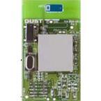
SmartMesh IP™ wireless sensor networks are self managing, low power Internet Protocol (IP) networks built
from wireless nodes called motes. The LTP™5901-IPM/
LTP5902-IPM is the IP mote product in the Eterna®* family
of IEEE 802.15.4e printed circuit board assembly solutions,
featuring a highly-integrated, low power radio design by
Dust Networks® as well as an ARM Cortex-M3 32-bit
microprocessor running Dust’s embedded SmartMesh IP
networking software. Both the LTP5901-IPM (with chip
antenna), at 24mm × 42mm, and the LTP5902-IPM (with
MMCX connector), at 24mm × 37mm, are designed for
surface mount assembly.
n
LTP5901-IPM/LTP5902-IPM
Features
Industry-Leading Low Power Radio Technology with
4.5mA to Receive and 9.7mA to Transmit at 8dBm
n RF Modular Certification Include USA, Canada, EU,
Japan, Taiwan, Korea, India, Australia and New Zealand
n PCB Assembly with Chip Antenna (LTP5901-IPM) or
with MMCX Antenna Connector (LTP5902-IPM). QFN
Version (LTC®5800-IPM) Available
n Micrium µCOS-II Real Time Operating System Based
On-Chip Software Development Kit
n
With Dust’s time-synchronized SmartMesh IP networks,
all motes in the network may route, source or terminate
data, while providing many years of battery powered
operation. The SmartMesh IP software provided with the
LTP5901-IPM/LTP5902-IPM is fully tested and validated,
and is readily configured via a software Application Programming Interface.
SmartMesh IP motes deliver a highly flexible network
with proven reliability and low power performance in an
easy-to-integrate platform.
L, LT, LTC, LTM, Linear Technology, the Linear logo, Dust, Dust Networks, SmartMesh and
Eterna are registered trademarks and LTP, the Dust Networks logo and SmartMesh IP are
trademarks of Linear Technology Corporation. All other trademarks are the property of their
respective owners. Protected by U.S. Patents, including 7375594, 7420980, 7529217, 7791419,
7881239, 7898322, 8222965.
* Eterna is Dust Networks’ low power radio SoC architecture.
Typical Application
LTP5901-IPM
LTP5901-IPR/
LTP5902-IPR
ANTENNA
IN+
LTC2379-18 SPI
SENSOR
µCONTROLLER
UART
UART
IN–
HOST
APPLICATION
59012ipm TA01
59012ipmfa
For more information www.linear.com/LTP5901-IPM or www.linear.com/LTP5902-IPM
1
�LTP5901-IPM/LTP5902-IPM
Table of Contents
Network Features........................................... 1
LTP5901-IPM/LTP5902-IPM Features.................... 1
Typical Application ......................................... 1
Description.................................................. 1
Table of Contents ........................................... 2
SmartMesh Network Overview............................ 3
Absolute Maximum Ratings............................... 4
Pin Configuration........................................... 4
Order Information........................................... 5
Recommended Operating Conditions.................... 5
DC Characteristics.......................................... 5
Radio Specifications....................................... 6
Radio Receiver Characteristics........................... 6
Radio Transmitter Characteristics........................ 7
Digital I/O Characteristics................................. 7
Temperature Sensor Characteristics..................... 8
Analog Input Chain Characteristics...................... 8
System Characteristics.................................... 8
UART AC Characteristics................................... 9
TIMEn AC Characteristics................................. 10
Radio_Inhibit AC Characteristics........................ 10
Flash AC Characteristics.................................. 11
Flash SPI Slave AC Characteristics..................... 11
SPI Master AC Characteristics........................... 12
I2C AC Characteristics..................................... 13
1-Wire Master.............................................. 13
Flash SPI Slave AC Characteristics..................... 14
Typical Performance Characteristics................... 15
Pin Functions............................................... 20
Operation................................................... 24
Power Supply........................................................... 24
Supply Monitoring and Reset..................................25
Precision Timing......................................................25
Application Time Synchronization...........................25
Time References......................................................25
Radio.......................................................................26
UARTs......................................................................26
Autonomous MAC.................................................... 27
Security................................................................... 27
Temperature Sensor................................................ 27
RADIO INHIBIT........................................................ 27
Software Installation................................................ 27
Flash Data Retention................................................ 28
State Diagram.......................................................... 28
I2C Master...............................................................30
SPI Master...............................................................30
1-Wire Master..........................................................30
Applications Information................................. 31
Modes of Operation................................................. 31
Regulatory and Standards Compliance.................... 31
Soldering Information.............................................. 32
Related Documentation................................... 32
Package Description...................................... 33
Revision History........................................... 35
Typical Application........................................ 36
Related Parts............................................... 36
59012ipmfa
2
For more information www.linear.com/LTP5901-IPM or www.linear.com/LTP5902-IPM
�LTP5901-IPM/LTP5902-IPM
SmartMesh Network Overview
A SmartMesh network consists of a self-forming multi-hop
mesh of nodes, known as motes, which collect and relay
data, and a network manager that monitors and manages
network performance and security, and exchanges data
with a host application.
SmartMesh networks communicate using a time slotted
channel hopping (TSCH) link layer, pioneered by Dust
Networks. In a TSCH network, all motes in the network
are synchronized to within less than a millisecond. Time
in the network is organized into time slots, which enables
collision-free packet exchange and per-transmission
channel-hopping. In a SmartMesh network, every device
has one or more parents (e.g. mote 3 has motes 1 and
2 as parents) that provide redundant paths to overcome
communications interruption due to interference, physical
obstruction or multi-path fading. If a packet transmission
fails on one path, the next retransmission may try on a
different path and different RF channel.
A network begins to form when the network manager
instructs its on-board Access Point (AP) radio to begin
sending advertisements—packets that contain information
that enables a device to synchronize to the network and
request to join. This message exchange is part of the security handshake that establishes encrypted communications
between the manager or application, and mote. Once motes
have joined the network, they maintain synchronization
through time corrections when a packet is acknowledged.
The Network Manager uses health reports to continually
optimize the network to maintain >99.999% data reliability
even in the most challenging RF environments.
The use of TSCH allows SmartMesh devices to sleep in
between scheduled communications and draw very little
power in this state. Motes are only active in time slots
where they are scheduled to transmit or receive, typically
resulting in a duty cycle of < 1%. The optimization software in the Network Manager coordinates this schedule
automatically. When combined with the Eterna low power
radio, every mote in a SmartMesh network—even busy
routing ones—can run on batteries for years. By default,
all motes in a network are capable of routing traffic from
other motes, which simplifies installation by avoiding the
complexity of having distinct routers vs non-routing end
nodes. Motes may be configured as non-routing to further
reduce that particular mote’s power consumption and to
support a wide variety of network topologies.
ALL NODES ARE ROUTERS.
THEY CAN TRANSMIT AND RECEIVE.
THIS NEW NODE CAN JOIN
ANYWHERE BECAUSE ALL
NODES CAN ROUTE.
HOST
APPLICATION
SNO 02
NETWORK MANAGER
AP
Mote
1
Mote
2
Mote
3
SNO 01
An ongoing discovery process ensures that the network
continually discovers new paths as the RF conditions
change. In addition, each mote in the network tracks performance statistics (e.g. quality of used paths, and lists of
potential paths) and periodically sends that information
to the network manager in packets called health reports.
At the heart of SmartMesh motes and network managers is the Eterna IEEE 802.15.4e System-on-Chip (SoC),
featuring Dust Networks’ highly integrated, low power
radio design, plus an ARM Cortex-M3 32-bit microprocessor running SmartMesh networking software. The
SmartMesh networking software comes fully compiled
yet is configurable via a rich set of Application Programming Interfaces (APIs) which allows a host application
to interact with the network, e.g. to transfer information
to a device, to configure data publishing rates on one or
more motes, or to monitor network state or performance
metrics. Data publishing can be uniform or different for
each device, with motes being able to publish infrequently
or faster than once per second as needed.
59012ipmfa
For more information www.linear.com/LTP5901-IPM or www.linear.com/LTP5902-IPM
3
�LTP5901-IPM/LTP5902-IPM
Absolute Maximum Ratings
Pin Configuration
(Note 1)
Pin functions shown in italics are currently not supported in software.
1
2
3
4
5
6
7
8
9
10
11
12
13
14
15
16
17
18
19
20
21
22
23
24
25
26
27
28
29
30
66
65
64
63
62
61
60
59
58
57
56
55
54
53
52
51
50
49
48
47
46
45
44
43
42
41
40
39
38
37
UARTC0_TX 31
UARTC0_RX 32
IPCS_MISO / GPIO6 33
CAUTION: This part is sensitive to electrostatic discharge
(ESD). It is very important that proper ESD precautions be
observed when handling the LTP5901-IPM/LTP5902-IPM.
GND
RESERVED
NC
GPIO17
GPIO18
GPIO19
AI_2
AI_1
AI_3
AI_0
GND
RESERVED
NC
NC
RESETn
TDI
TDO
TMS
TCK
GND
DP4 (GPIO23)
RESERVED
RESERVED
RESERVED
DP3 (GPIO22) / TIMER8_IN
DP2 (GPIO21) / LPTIMER_IN
SLEEPn / GPIO14
DP0 (GPIO0) / SPIM_SS_2n
NC
GND
GND
NC
RADIO_INHIBIT / GPIO15
TIMEn / GPIO1
UART_TX
UART_TX_CTSn
UART_TX_RTSn
UART_RX
UART_RX_CTSn
UART_RX_RTSn
GND
VSUPPLY
RESERVED
NC
NC
FLASH_P_ENn / GPIO2
SPIS_SSn / SDA
SPIS_SCK / SCL
SPIS_MOSI / GPIO26 / UARTC1_RX
SPIS_MISO / 1_WIRE / UARTC1_TX
PWM0 / GPIO16
DP1 (GPIO20) / TIMER16_IN
SPIM_SS_0n / GPIO12
SPIM_SS_1n / GPIO13
GND
SPIM_SCK / GPIO9
SPIM_MOSI / GPIO10
IPCS_SSn / GPIO3
SPIM_MISO / GPIO11
GND
GND 34
IPCS_MOSI / GPIO5 35
IPCS_SCK / GPIO4 36
Supply Voltage on VSUPPLY...................................4.20V
Input Voltage on AI_0/1/2/3 Inputs.........................1.98V
Voltage on Any Digital
I/O pin..................................... –0.3V to VSUPPLY + 0.3V
Input RF Level..................................................... +10dBm
Storage Temperature Range (Note 3)...... –55°C to 105°C
Operating Temperature Range
LTP5901I/LPT5902I..............................–40°C to 85°C
PC PACKAGE
66-LEAD PCB
59012ipmfa
4
For more information www.linear.com/LTP5901-IPM or www.linear.com/LTP5902-IPM
�LTP5901-IPM/LTP5902-IPM
Order Information
LEAD FREE FINISH†
PART MARKING*
PACKAGE DESCRIPTION
TEMPERATURE RANGE
LTP5901IPC-IPMA#PBF
LTP5901IPC-IPMA#PBF
66-Lead (42mm × 24mm × 5.5mm) PCB with Chip Antenna
–40°C to 85°C
LTP5902IPC-IPMA#PBF
LTP5902IPC-IPMA#PBF
66-Lead (37.5mm × 24mm × 5.5mm) PCB with MMCX Connector –40°C to 85°C
†This product ships with the flash erased at the time of order. OEMs will need to program devices during development and manufacturing.
For legacy part numbers and ordering information go to: http://www.linear.com/product/LTP5901-IPM#orderinfo or
http://www.linear.com/product/LTP5902-IPM#orderinfo
*The temperature grade is identified by a label on the shipping container.
For more information on lead free part marking, go to: http://www.linear.com/leadfree/
Recommended Operating Conditions
The l denotes the specifications which apply over
the full operating temperature range, otherwise specifications are at TA = 25°C and VSUPPLY = 3.6V unless otherwise noted.
SYMBOL
PARAMETER
CONDITIONS
MIN
TYP
VSUPPLY
Supply Voltage
Including Noise and Load Regulation
l
Supply Noise
50Hz to 2MHz
l
250
mV
Operating Relative Humidity
Non-Condensing
l
10
90
% RH
Temperature Ramp Rate
While Operating in Network
l
–8
+8
°C/min
2.1
MAX
UNITS
3.76
V
DC Characteristics
The l denotes the specifications which apply over the full operating temperature range,
otherwise specifications are at TA = 25°C and VSUPPLY = 3.6V unless otherwise noted.
OPERATION/STATE
CONDITIONS
Power-on Reset
During Power-On Reset, Maximum 750µs + VSUPPLY Rise Time
from 1V to 1.9V
MIN
TYP
12
MAX
UNITS
mA
Doze
RAM on, ARM Cortex-M3, Flash, Radio, and Peripherals Off, All
Data and State Retained, 32.768kHz Reference Active
1.2
µA
Deep Sleep
RAM on, ARM Cortex-M3, Flash, Radio, and Peripherals Off, All
Data and State Retained, 32.768kHz Reference Inactive
0.8
µA
In-Circuit Programming
RESETn and FLASH_P_ENn Asserted, IPCS_SCK at 8MHz
20
mA
Peak Operating Current
+8dBm
+0dBm
System Operating at 14.7MHz, Radio Transmitting, During Flash
Write. Maximum Duration 4.33 ms.
30
26
mA
mA
Active
ARM Cortex M3, RAM and Flash Operating, Radio and All Other
Peripherals Off. Clock Frequency of CPU and Peripherals Set to
7.3728MHz, VCORE = 1.2V
1.3
mA
Flash Write
Single Bank Flash Write
3.7
mA
Flash Erase
Single Bank Page or Mass Erase
2.5
mA
Radio Tx
+0dBm
+8dBm
Current with Autonomous MAC Managing Radio Operation,
CPU Inactive. Clock Frequency of CPU and Peripherals Set to
7.3728MHz.
5.4
9.7
mA
mA
Radio Rx
Current with Autonomous MAC Managing Radio Operation,
CPU Inactive. Clock Frequency of CPU and Peripherals Set to
7.3728MHz.
4.5
mA
59012ipmfa
For more information www.linear.com/LTP5901-IPM or www.linear.com/LTP5902-IPM
5
�LTP5901-IPM/LTP5902-IPM
Radio Specifications
The l denotes the specifications which apply over the full operating temperature range,
otherwise specifications are at TA = 25°C and VSUPPLY = 3.6V unless otherwise noted.
PARAMETER
CONDITIONS
MIN
TYP
2.4000
MAX
UNITS
2.4835
GHz
Frequency Band
l
Number of Channels
l
15
Channel Separation
l
5
MHz
l
2405 + 5•(k-11)
MHz
l
250
kbps
Channel Center Frequency
Where k = 11 to 25, as Defined by IEEE 802.15.4
Modulation
IEEE 802.15.4 Direct Sequence Spread Spectrum (DSSS)
Raw Data Rate
Antenna Pin ESD Protection
HBM per JEDEC JESD22-A114F (Note 2)
Range (Note 4)
Indoor
Outdoor
Free Space
25°C, 50% RH, +2dBi Omni-Directional Antenna, Antenna 2m
Above Ground
±6000
V
100
300
1200
m
m
m
Radio Receiver Characteristics
The l denotes the specifications which apply over the full
operating temperature range, otherwise specifications are at TA = 25°C and VSUPPLY = 3.6V unless otherwise noted.
PARAMETER
CONDITIONS
Receiver Sensitivity
Packet Error Rate (PER) = 1% (Note 5)
MIN
–93
dBm
Receiver Sensitivity
PER = 50%
–95
dBm
Saturation
Maximum Input Level the Receiver Will
Properly Receive Packets
0
dBm
Adjacent Channel Rejection (High Side) Desired Signal at –82dBm, Adjacent Modulated Channel 5MHz
Above the Desired Signal, PER = 1% (Note 5)
22
dBc
Adjacent Channel Rejection (Low Side) Desired Signal at –82dBm, Adjacent Modulated Channel 5MHz
Below the Desired Signal, PER = 1% (Note 5)
19
dBc
Alternate Channel Rejection
(High Side)
Desired Signal at –82dBm, Alternate Modulated Channel 10MHz
Above the Desired Signal, PER = 1% (Note 5)
40
dBc
Alternate Channel Rejection (Low Side) Desired Signal at –82dBm, Alternate Modulated Channel 10MHz
Below the Desired Signal, PER = 1% (Note 5)
36
dBc
Second Alternate Channel Rejection
Desired Signal at –82dBm, Second Alternate Modulated Channel
Either 15MHz Above or Below, PER = 1% (Note 5)
42
dBc
Co-Channel Rejection
Desired Signal at –82dBm, Undesired Signal is an 802.15.4
Modulated Signal at the Same Frequency, PER = 1%
–6
dBc
LO Feed Through
–55
dBm
Frequency Error Tolerance (Note 6)
±50
ppm
Symbol Error Tolerance
Received Signal Strength Indicator
(RSSI) Input Range
TYP
MAX
UNITS
±50
ppm
–90 to –10
dBm
RSSI Accuracy
±6
dB
RSSI Resolution
1
dB
59012ipmfa
6
For more information www.linear.com/LTP5901-IPM or www.linear.com/LTP5902-IPM
�LTP5901-IPM/LTP5902-IPM
Radio Transmitter Characteristics
The l denotes the specifications which apply over the
full operating temperature range, otherwise specifications are at TA = 25°C and VSUPPLY = 3.6V unless otherwise noted.
PARAMETER
CONDITIONS
Output Power
High Calibrated Setting
Low Calibrated Setting
Delivered to a 50Ω load
Spurious Emissions
Conducted Measurement with a 50Ω Single-Ended Load,
+8dBm Output Power. All Measurements Made with Max
Hold.
30MHz to 1000MHz
1GHz to 12.75GHz
2.4GHz ISM Upper Band Edge (Peak)
2.4GHz ISM Upper Band Edge (Average)
2.4GHz ISM Lower Band Edge
RBW = 120kHz, VBW = 100Hz
RBW = 1MHz, VBW = 3MHz
RBW = 1MHz, VBW = 3MHz
RBW = 1MHz, VBW = 10Hz
RBW = 100kHz, VBW = 100kHz
Harmonic Emissions
2nd Harmonic
3rd Harmonic
Conducted Measurement Delivered to a 50Ω Load,
Resolution Bandwidth = 1MHz, Video Bandwidth = 1MHz
MIN
TYP
MAX
UNITS
8
0
dBm
dBm
85°C
can be approximated by calculating the dimensionless
acceleration factor using the following equation.
AF = e
Ea
1
1
−
•
k TUSE +273 TSTRESS +273
State Diagram
In order to provide capabilities and flexibility in addition
to ultralow power, Eterna operates in various states, as
shown in Figure 11. Eterna State Diagram and described
in this section. State transitions shown in red are not
recommended.
Start-Up
Start-up occurs as a result of either crossing the power-on
reset threshold or asserting RESETn. After the completion
of power-on reset or the falling edge of an internally
synchronized RESETn, Eterna loads its fuse table which,
as described in the previous section, includes setting
I/O direction. In this state, Eterna checks the state of
the FLASH_P_ENn and RESETn and enters the serial
flash emulation mode if both signals are asserted. If the
FLASH_P_ENn pin is not asserted but RESETn is asserted,
Eterna automatically reduces its energy consumption to
a minimum until RESETn is released. Once RESETn is
de-asserted, Eterna goes through a boot sequence, and
then enters the active state.
Where:
Serial Flash Emulation
AF = acceleration factor
When both RESETn and FLASH_P_ENn are asserted,
Eterna disables normal operation and enters a mode to
emulate the operation of a serial flash. In this mode, its
flash can be programmed.
Ea = activation energy = 0.6eV
k = 8.625 • 10–5eV/°K
TUSE = is the specified temperature retention in °C
TSTRESS = actual storage temperature in °C
Example: Calculate the effect on retention when storing
at a temperature of 105°C.
TSTRESS = 105°C
TUSE = 85°C
AF = 2.8
So the overall retention of the flash would be degraded
by a factor of 2.8, reducing data retention from 20 years
at 85°C to 7.1 years at 105°C.
Operation
Once Eterna has completed start-up, Eterna transitions to
the operational group of states (active/CPU active, active/
CPU inactive, and Doze). There, Eterna cycles between the
various states, automatically selecting the lowest possible power state while fulfilling the demands of network
operation.
Active State
In the active state, Eterna’s relaxation oscillator is running
and peripherals are enabled as needed. The ARM Cortex-M3
59012ipmfa
28
For more information www.linear.com/LTP5901-IPM or www.linear.com/LTP5902-IPM
�LTP5901-IPM/LTP5902-IPM
Operation
cycles between CPU-active and CPU-inactive (referred
to in the ARM Cortex-M3 literature as sleep now mode).
Eterna’s extensive use of DMA and intelligent peripherals
that independently move Eterna between active state and
doze state minimizes the time the CPU is active, significantly reducing Eterna’s energy consumption.
POWER-ON
RESET
Doze State
The doze state consumes orders of magnitude less current than the active state and is entered when all of the
peripherals and the CPU are inactive. In the doze state
Eterna’s full state is retained, timing is maintained, and
Eterna is configured to detect, wake, and rapidly respond
to activity on I/Os (such as UART signals and the TIMEn
pin). In the doze state the 32.768kHz oscillator and associated timers are active.
VSUPPLY > PoR
RESETn LOW AND
FLASH_P_ENn LOW
LOAD FUSE
SETTINGS
RESETn LOW AND
FLASH_P_ENn HIGH
SET RESETn HIGH AND
FLASH_P_ENn HIGH
FOR 125µs, THEN
SET RESETn LOW
SERIAL FLASH
EMULATION
RESETn HIGH
AND
FLASH_P_ENn
HIGH
RESET
DEASSERT
RESETn
BOOT
START-UP
ASSERT RESETn
DOZE
ASSERT RESETn
CPU AND
PERIPHERALS
INACTIVE
HW OR PMU EVENT
OPERATION
ASSERT RESETn
CPU
ACTIVE
ACTIVE
CPU
INACTIVE
DEEP SLEEP
LOW POWER SLEEP
COMMAND
INACTIVE
59012ipm F15
Figure 15. Eterna State Diagram
59012ipmfa
For more information www.linear.com/LTP5901-IPM or www.linear.com/LTP5902-IPM
29
�LTP5901-IPM/LTP5902-IPM
Operation
I2C Master
The I2C Master enables control of I2C slave devices,
including support for clock stretching slaves. I2C Multimaster and bus arbitration protocols are not supported.
For implementation details refer to the On-Chip Software
Development Kit (On-Chip SDK).
SPI Master
The Eterna SPI master controller supports all configurations
of clock polarity and phase, supporting shift clock frequencies of 460.8kHz, 921.6kHz, 1.8432MHz, or 3.6864MHz.
In addition the SPI master controller can be configured to
repetitively issue commands and capture the correspond-
ing output, enabling repetitive sampling of signals from a
SPI ADC or SPI sensor based upon a clock reference of
better than ±50ppm. For implementation details refer to
the On-Chip Software Development Kit (On-Chip SDK).
1-Wire Master
The Eterna 1-Wire Master controller supports the reset,
presence detect, read and write 1-Wire protocol operations,
incorporating an active pull-up. The active pull-up becomes
active when the passive pull-up raises the voltage on the
1_WIRE pin nominally above 1.4V, driving the 1_WIRE
signal as specified in Digital I/O Characteristics. For
implementation details refer to the On-Chip Software
Development Kit (On-Chip SDK).
59012ipmfa
30
For more information www.linear.com/LTP5901-IPM or www.linear.com/LTP5902-IPM
�LTP5901-IPM/LTP5902-IPM
Applications Information
Modes of Operation
General Purpose Input-Output (GPIO) pins
n Analog-to-Digital Converter (ADC)
n Universal Asynchronous Receiver/Transmitter
(UART)
n Serial Peripheral Interface (SPI) Master
n Inter-Integrated Circuit (I2C) Master
n
The SmartMesh IP Mote software can be operated in three
distinct modes, namely, namely Slave, Master, and OnChip SDK. Mode selection should be considered during
the architecture/design phase of the development process.
Slave Mode
In Slave mode, the Eterna is connected to an external
microprocessor through the API UART and is solely used
as a networking device. None of the built in I/Os are accessible in this mode. Refer to the SmartMesh IP User's
Guide for more detailed information.
Master Mode
In Master mode, no external µProcessor is required and a
limited set of functionality is made available with no programming required on the device. The following features
are available
n On-Chip Temperature Sensor
n 4 Analog Inputs
n 4 Digital Inputs
n 3 Digital Outputs
Refer to the SmartMesh IP User's Guide for more detailed
information.
On-Chip SDK (OCSDK)
The SmartMesh IP On-Chip Software Development Kit (OnChip SDK) enables development of C-code applications for
execution on the LTC5800-IPM, running Micrium’s µCOS-II
real-time operating system. With the On-Chip SDK, users
may quickly and easily develop application code without
the need for an external microprocessor.
Applications written within the On-Chip SDK may send
and receive wireless messages through the mesh network;
process data, such as statistical analysis; execute local
decision-making and control; and manage the following
peripherals:
1-Wire Master
n
Network connectivity and quality of service is handled by
the SmartMesh IP protocol stack. The SmartMesh IP stack
comes as a pre-compiled library and delivers >99.999%
data reliability while providing ultra low power operation.
Regulatory and Standards Compliance
Radio Certification
The LTP5901 and LTP5902 have been certified under a
single modular certification, with the module name of
ETERNA2. Following the regulatory requirements provided in the ETERNA2 User’s Guide enables customers
to ship products in the supported geographies, by simply
completing an unintentional radiator scan of the finished
product(s). The ETERNA2 User’s Guide also provides
the technical information needed to enable customers
to further certify either the modules or products based
upon the modules in geographies that have not or do not
support modular certification.
Compliance to Restriction of Hazardous Substances
(RoHS)
Restriction of Hazardous Substances 2 (RoHS 2) is a
directive that places maximum concentration limits on
the use of certain hazardous substances in electrical and
electronic equipment. Linear Technology is committed to
meeting the requirements of the European Community
directive 2011/65/EU.
59012ipmfa
For more information www.linear.com/LTP5901-IPM or www.linear.com/LTP5902-IPM
31
�LTP5901-IPM/LTP5902-IPM
Applications Information
This product has been specifically designed to utilize
RoHS-compliant materials and to eliminate or reduce the
use of restricted materials to comply with 2011/65/EU.
The RoHS-compliant design features include:
RoHS-compliant solder for solder joints
Note: Customers may elect to use certain types of leadfree solder alloys in accordance with the European Community directive 2011/65/EU. Depending on the type of
solder paste chosen, a corresponding process change to
optimize reflow temperatures may be required.
n
RoHS-compliant base metal alloys
Soldering Information
RoHS-compliant precious metal plating
The LTP5901 and LTP5902 are suitable for both eutectic
PbSn and RoHS-6 reflow. The maximum reflow soldering temperature is 260°C. A more detailed description of
layout recommendations, assembly procedures and design
considerations is included in the LTP5901 and LTP5902
Hardware Integration Guide.
n
n
RoHS-compliant cable assemblies and connector
choices
n
RoHS-compliant and 245°C reflow compatible
n
Related Documentation
TITLE
LOCATION
DESCRIPTION
SmartMesh IP Users Guide
http://www.linear.com/docs/41880
Theory of operation for SmartMesh IP networks and motes
SmartMesh IP Mote API Guide
http://www.linear.com/docs/41886
Definitions of the applications interface commands available over
the API UART
SmartMesh IP Mote CLI Guide
http://www.linear.com/docs/41885
Definitions of the command line interface commands available
over the CLI UART
LTP5901 and LTP5902 Hardware
Integration Guide
http://www.linear.com/docs/41877
Recommended practices for designing with the LTP5901 and
LTP5902
ETERNA2 User’s Guide
http://www.linear.com/docs/42916
The ETERNA2 module user’s guide includes certification
requirements applicable to certified geographies and support
documentation enabling customer certification in additional
geographies for the LTP5901 and LTP5902
SmartMesh IP Tools Guide
http://www.linear.com/docs/42453
The user’s guide for all IP related tools, and specifically the
definition for the On-chip Application Protocol (OAP)
59012ipmfa
32
For more information www.linear.com/LTP5901-IPM or www.linear.com/LTP5902-IPM
�LTP5901-IPM/LTP5902-IPM
Package Description
Please refer to http://www.linear.com/product/LTP5901#packaging for the most recent package drawings.
1
2
4
3
5
PC Package
66-Lead PCB (24mm × 42mm)
(Reference LTC DWG # 05-08-10002 Rev A)
D
.100
2.54
.039
1.00
.945
24.00
.039
1.00
1.57
40.00
.039
1.00
C
1.213
30.80
1.122
28.50
1.102
28.00
1.063
27.00
1.031
26.20
R.010 TYP
0.25
1.654
42.00
.039 TYP
1.00
B
.079
2.00
4X
.039
1.00
.035
0.90
0
0.00
.039
1.00
.87
22.00
.728
18.50
.630
16.00
.591
15.00
.551
14.00
.444
11.28
.394
10.00
.197
5.00
.236
6.00
.344
8.74
A
0
0.00
.157
4.00
.039
1.00
.08
2.00
.08
2.00
LTP5901 Mechanical Drawing
1
2
3
PROPRIETARY AND CONFIDENTIAL
THE INFORMATION CONTAINED IN THIS DRAWING IS THE S
PROPERTY OF LINEAR INCORPORATED. ANY REPRODUCT
IN PART OR AS A WHOLE WITHOUT THE WRITTEN PERMISS
OF LINEAR INCORPORATED IS PROHIBITED.
4
5
59012ipmfa
For more information www.linear.com/LTP5901-IPM or www.linear.com/LTP5902-IPM
33
�LTP5901-IPM/LTP5902-IPM
Package Description
Please refer to http://www.linear.com/product/LTP5902#packaging for the most recent package drawings.
1
2
4
3
5
6
PC Package
66-Lead PCB (24mm × 37.5mm)
(Reference LTC DWG # 05-08-10003 Rev A)
D
.100
2.54
.177
4.50
.039
1.00
.945
24.00
.039
1.00
.029
0.73
1.40
35.50
1.272
32.30
C
.039
1.00
1.213
30.80
1.122
28.50
1.102
28.00
1.063
27.00
1.031
26.20
R.010 TYP
0.25
1.476
37.50
.039 TYP
1.00
B
4X
.035
0.90
.079
2.00
.039
1.00
0
0.00
.866
22.00
.591
15.00
.630
16.00
.728
18.50
.551
14.00
.394
10.00
.444
11.28
.344
8.73
.197
5.00
.236
6.00
.157
4.00
A
0
0.00
.071
1.80
.039
1.00
.078
2.0
.039
1.00
.079
2.01
DRN BY:
CHK:
APPD:
LTP5902 Mechanical Drawing
1
2
3
APPD:
PROPRIETARY AND CONFIDENTIAL
4
THE INFORMATION CONTAINED IN THIS DRAWING IS THE SOLE
PROPERTY OF LINEAR TECHNOLOGY CORPORATION. ANY
REPRODUCTION IN PART OR AS A WHOLE WITHOUT THE
WRITTEN PERMISSION OF LINEAR TECHNOLOGY
CORPORATION IS PROHIBITED.
5
6
59012ipmfa
34
For more information www.linear.com/LTP5901-IPM or www.linear.com/LTP5902-IPM
PROJ MGR
PROD R
ENG
�LTP5901-IPM/LTP5902-IPM
Revision History
REV
DATE
DESCRIPTION
A
11/15
Updated ordering part number
PAGE NUMBER
Added On-Chip SDK section
Added Software Installation section
5
23, 30, 31
27
59012ipmfa
Information furnished by Linear Technology Corporation is believed to be accurate and reliable.
However, no responsibility is assumed for its use. Linear Technology Corporation makes no representationmore
that theinformation
interconnection
of its circuits as described herein will
infringe on existing patent rights.
For
www.linear.com/LTP5901-IPM
or not
www.linear.com/LTP5902-IPM
35
�LTP5901-IPM/LTP5902-IPM
Typical Application
Mesh Network Thermistor
TADIRAN TL-5903
Li-SOCI2
LTP5902-IPM
ANTENNA
VSUPPLY
LT6654
VIN
IPCS_MISO
VOUT
0.1µF
0.1µF
GND2
5k
0.1%
AI_0
1000pF
59012ipm TA02
10k, 0.2C
OMEGA 4406
5k
0.1%
AI_1
GND
GND1
1000pF
5k
0.1%
RT = 5k • AI_0 / (2 • AI_1 – AI_0)
T(°C) = 1 / {A + B [Ln(RT)] + C[Ln(RT)]3} – 273.15
A = 1.032 • 10–3
B = 2.387 • 10–4
C = 1.580 • 10–7
Related Parts
PART NUMBER DESCRIPTION
COMMENTS
LTC5800-IPM
IP Wireless Mote
Ultralow Power Mote, 72-Lead 10mm × 10mm QFN
LTP5901-IPR
IP Wireless Mesh Manager PCB Module with Chip Includes Modular Radio Certification in the United States, Canada, Europe, Japan,
Antenna
South Korea, Taiwan, India, Australia and New Zealand
LTP5902-IPR
IP Wireless Mesh Manager PCB Module with
MMCX Antenna Connector
LT6654
Precision High Output Drive Low Noise Reference 1.6ppm Peak-to-Peak Noise (0.1Hz to 10Hz, Sink/Source ±10mA, 5ppm/°C Max Drift
LTC2379-18
18-Bit,1.6Msps/1Msps/500ksps/250ksps Serial,
Low Power ADC
2.5V Supply, Differential Input, 101.2dB SNR, ±5V Input Range, DGC
LTC3388-1/
LTC3388-3
20V High Efficiency Nanopower Step-Down
Regulator
860nA IQ in Sleep, 2.7V to 20V Input, VOUT = 1.2V to 5V, Enable and Standby Pins
LTC3588-1
Piezoelectric Energy Generator with Integrated
High Efficiency Buck Converter
VIN = 2.7V to 20V, VOUT(MIN) = Fixed to 1.8V/2.5V/3.3V/3.6V, IQ = 0.95μA,
3mm × 3mm DFN-10 and MSOP-10E Packages
LTC3108-1
Ultralow Voltage Step-Up Converter and Power
Manager
VIN = 0.02V to 1V, VOUT = 2.5V/3V/3.7V/4.5V Fixed, IQ = 6μA, 3mm × 4mm DFN-12
and SSOP-16 Packages
LTC3459
Micropower Synchronous Boost Converter
VIN = 1.5V to 5.5V, VOUT(MAX) = 10V, IQ = 10μA, 2mm × 2mm DFN,
2mm × 3mm DFN or SOT-23 Package
Includes Modular Radio Certification in the United States, Canada, Europe, Japan,
South Korea, Taiwan, India, Australia and New Zealand
59012ipmfa
36 Linear Technology Corporation
1630 McCarthy Blvd., Milpitas,
CA 95035-7417
For more information
www.linear.com/LTP5901-IPM or www.linear.com/LTP5902-IPM
(408) 432-1900 ● FAX: (408) 434-0507
●
www.linear.com/LTP5901-IPM or www.linear.com/LTP5902-IPM
LT 1115 REV A • PRINTED IN USA
LINEAR TECHNOLOGY CORPORATION 2014
�


 工商网监
湘ICP备2023018690号
工商网监
湘ICP备2023018690号

