LESHAN RADIO COMPANY, LTD.
Bias Resistor Transistors
PNP Silicon Surface Mount Transistors with Monolithic Bias Resistor Network
This new series of digital transistors is designed to replace a single device and its external resistor bias network. The BRT (Bias Resistor Transistor) contains a single transistor with a monolithic bias network consisting of two resistors; a series base resistor and a base-emitter resistor. The BRT eliminates these individual components by integrating them into a single device. The use of a BRT can reduce both system cost and board space. The device is housed in the SOT-23 package which is designed for low power surface mount applications.
MMUN2111LT1 Series
MMUN2111LT1 SERIES
3 1 2
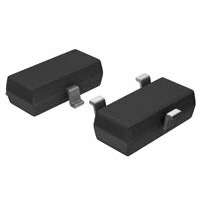
CASE 318, STYLE 6 SOT–23 (TO–236AB)
• • • • •
Simplifies Circuit Design Reduces Board Space Reduces Component Count The SOT-23 package can be soldered using wave or reflow. The modified gull-winged leads absorb thermal stress during soldering eliminating the possibility of damage to the die. Available in 8 mm embossed tape and reel. Use the Device Number to order the 7 inch/3000 unit reel. Replace “T1” with “T3” in the Device Number to order the 13 inch/10,000 unit reel.
PIN 1 BASE (INPUT)
R1
PIN 3 COLLECTOR (OUTPUT)
R2
PIN 2 EMITTER (GROUND)
MARKINGDIAGRAM
A6x M
MAXIMUM RATINGS (TA = 25°C unless otherwise noted)
Rating Collector-Base Voltage Collector-Emitter Voltage Collector Current Symbol VCBO VCEO IC Value 50 50 100 Unit Vdc Vdc mAdc
A6x = Device Marking x M = A – L(See Page 2) = Date Code
DEVICE MARKING INFORMATION
See specific marking information in the device marking table on page 2 of this
THERMAL CHARACTERISTICS
Characteristic Total Device Dissipation TA = 25°C Derate above 25°C Thermal Resistance – Junction-to-Ambient Thermal Resistance – Junction-to-Lead Junction and Storage Temperature Range 1. FR–4 @ Minimum Pad 2. FR–4 @ 1.0 x 1.0 inch Pad Symbol PD Max 246 (Note 1.) 400 (Note 2.) 1.5 (Note 1.) 2.0 (Note 2.) 508 (Note 1.) 311 (Note 2.) 174 (Note 1.) 208 (Note 2.) –55 to +150 Unit mW °C/W °C/W °C/W °C
data sheet.
RθJA RθJL TJ, Tstg
MMUN2111S-1/11
�LESHAN RADIO COMPANY, LTD.
MMUN2111LT1 Series
DEVICE MARKING AND RESISTOR VALUES
Device MMUN2111LT1 MMUN2111LT3 MMUN2112LT1 MMUN2112LT3 MMUN2113LT1 MMUN2113LT3 MMUN2114LT1 MMUN2114LT3 MMUN2115LT1 (Note 3.) MMUN2115LT3 MMUN2116LT1 (Note 3.) MMUN2116LT3 MMUN2130LT1 (Note 3.) MMUN2130LT3 MMUN2131LT1 (Note 3.) MMUN2131LT3 MMUN2132LT1 (Note 3.) MMUN2132LT3 MMUN2133LT1 (Note 3.) MMUN2133LT3 MMUN2134LT1 (Note 3.) MMUN2134LT3 Package SOT–23 SOT–23 SOT–23 SOT–23 SOT–23 SOT–23 SOT–23 SOT–23 SOT–23 SOT–23 SOT–23 Marking A6A A6B A6C A6D A6E A6F A6G A6H A6J A6K A6L R1 (K) 10 22 47 10 10 4.7 1.0 2.2 4.7 4.7 22 R2 (K) 10 22 47 47 ∞ ∞ 1.0 2.2 4.7 47 47 Shipping 3000/Tape & Reel 10,000/Tape & Reel 3000/Tape & Reel 10,000/Tape & Reel 3000/Tape & Reel 10,000/Tape & Reel 3000/Tape & Reel 10,000/Tape & Reel 3000/Tape & Reel 10,000/Tape & Reel 3000/Tape & Reel 10,000/Tape & Reel 3000/Tape & Reel 10,000/Tape & Reel 3000/Tape & Reel 10,000/Tape & Reel 3000/Tape & Reel 10,000/Tape & Reel 3000/Tape & Reel 10,000/Tape & Reel 3000/Tape & Reel 10,000/Tape & Reel
ELECTRICAL CHARACTERISTICS (TA = 25°C unless otherwise noted)
Characteristic Symbol Min Typ Max Unit
OFF CHARACTERISTICS
Collector-Base Cutoff Current (VCB = 50 V, IE = 0) Collector-Emitter Cutoff Current (VCE = 50 V, IB = 0) Emitter-Base Cutoff Current (V EB = 6.0 V, IC = 0 ) MMUN2111LT1 MMUN2112LT1 MMUN2113LT1 MMUN2114LT1 MMUN2115LT1 MMUN2116LT1 MMUN2130LT1 MMUN2131LT1 MMUN2132LT1 MMUN2133LT1 MMUN2134LT1 ICBO ICEO IEBO – – – – – – – – – – – – – 50 50 – – – – – – – – – – – – – – – 100 500 0.5 0.2 0.1 0.2 0.9 1.9 4.3 2.3 1.5 0.18 0.13 – – nAdc nAdc mAdc
Collector-Base Breakdown Voltage (IC = 10 µA, IE = 0) Collector-Emitter Breakdown Voltage (Note 4.) (IC = 2.0 mA, IB = 0) 3. New devices. Updated curves to follow in subsequent data sheets. 4. Pulse Test: Pulse Width < 300 µs, Duty Cycle < 2.0%
V(BR)CBO V(BR)CEO
Vdc Vdc
MMUN2111S–2/11
�LESHAN RADIO COMPANY, LTD.
MMUN2111LT1 Series
ELECTRICAL CHARACTERISTICS (TA = 25°C unless otherwise noted) (Continued)
Characteristic Symbol Min Typ Max Unit
ON CHARACTERISTICS (Note 5.)
DC Current Gain (V CE = 10 V, IC = 5.0 mA ) MMUN2111LT1 MMUN2112LT1 MMUN2113LT1 MMUN2114LT1 MMUN2115LT1 MMUN2116LT1 MMUN2130LT1 MMUN2131LT1 MMUN2132LT1 MMUN2133LT1 MMUN2134LT1 hFE 35 60 80 80 160 160 3.0 8.0 15 80 80 – 60 100 140 140 250 250 5.0 15 27 140 130 – – – – – – – – – – – – 0.25 Vdc
Collector-Emitter Saturation Voltage (IC = 10 mA, IE = 0.3 mA) (IC = 10 mA, IB = 5 mA) MMUN2130LT1/MMUN2131LT1 (IC = 10 mA, IB = 1 mA) MMUN2115LT1/MMUN2116LT1/ MMUN2132LT1/MMUN2133LT1/MMUN2134LT1 Output Voltage (on) (V CC = 5.0 V, VB = 2.5 V, RL = 1.0 kΩ ) MMUN2111LT1 MMUN2112LT1 MMUN2114LT1 MMUN2115LT1 MMUN2116LT1 MMUN2130LT1 MMUN2131LT1 MMUN2132LT1 MMUN2133LT1 MMUN2134LT1 MMUN2113LT1
VCE(sat)
VOL – – – – – – – – – – – VOH 4.9 – – – – – – – – – – – – 0.2 0.2 0.2 0.2 0.2 0.2 0.2 0.2 0.2 0.2 0.2 –
Vdc
(V
CC =
5.0 V, VB = 3.5 V, RL = 1.0 kΩ )
Output Voltage (off) (VCC = 5.0 V, VB = 0.5 V, RL = 1.0 kΩ) (VCC = 5.0 V, VB = 0.25 V, RL = 1.0 kΩ )
Vdc
(VCC
MMUN2115LT1 MMUN2116LT1 MMUN2131LT1 MMUN2132LT1 = 5.0 V, VB = 0.050 V, RL = 1.0 kΩ ) MMUN2130LT1 MMUN2111LT1 MMUN2112LT1 MMUN2113LT1 MMUN2114LT1 MMUN2115LT1 MMUN2116LT1 MMUN2130LT1 MMUN2131LT1 MMUN2132LT1 MMUN2133LT1 MMUN2134LT1 R1 7.0 15.4 32.9 7.0 7.0 3.3 0.7 1.5 3.3 3.3 15.4 0.8 0.17 – 0.8 0.055 10 22 47 10 10 4.7 1.0 2.2 4.7 4.7 22 1.0 0.21 – 1.0 0.1 13 28.6 61.1 13 13 6.1 1.3 2.9 6.1 6.1 28.6 1.2 0.25 – 1.2 0.185 kΩ
Input Resistor
Resistor Ratio MMUN2111LT1/MMUN2112LT1/MMUN2113LT1 MMUN2114LT1 MMUN2115LT1/MMUN2116LT1 MMUN2130LT1/MMUN2131LT1/MMUN2132LT1 MMUN2133LT1 5. Pulse Test: Pulse Width < 300 µs, Duty Cycle < 2.0%
R1/R2
MMUN2111S–3/11
�LESHAN RADIO COMPANY, LTD.
MMUN2111LT1 Series
TYPICAL ELECTRICAL CHARACTERISTICS MMUN2111LT1
250 PD , POWER DISSIPATION (MILLIWATTS) 200 VCE(sat) , MAXIMUM COLLECTOR VOLTAGE (VOLTS) 1 IC/IB = 10 TA = -25°C 75°C 0.1 25°C
150 100 50 0 -50 RθJA = 625°C/W
0
50
100
150
0.01
0
20
40
60
80
TA, AMBIENT TEMPERATURE (°C)
IC, COLLECTOR CURRENT (mA)
Figure 1. Derating Curve
1000 h FE, DC CURRENT GAIN (NORMALIZED) VCE = 10 V 4
Figure 2. VCE(sat) versus IC
100
TA = 75°C 25°C -25°C
Cob , CAPACITANCE (pF)
3
f = 1 MHz lE = 0 V TA = 25°C
2
1
10
1
10 IC, COLLECTOR CURRENT (mA)
100
0
0
10 20 30 40 VR, REVERSE BIAS VOLTAGE (VOLTS)
50
Figure 3. DC Current Gain
100
Figure 4. Output Capacitance
75°C
25°C TA = -25°C
100 VO = 0.2 V Vin, INPUT VOLTAGE (VOLTS) TA = -25°C 25°C 75°C 1
IC , COLLECTOR CURRENT (mA)
10 1
10
0.1
0.01 0.001 0 1 2
VO = 5 V 3 4 5 6 7 Vin, INPUT VOLTAGE (VOLTS) 8 9 10
0.1
0
10
20 30 IC, COLLECTOR CURRENT (mA)
40
50
Figure 5. Output Current versus Input Voltage
Figure 6. Input Voltage versus Output Current
MMUN2111S–4/11
�LESHAN RADIO COMPANY, LTD.
MMUN2111LT1 Series
TYPICAL ELECTRICAL CHARACTERISTICS MMUN2112LT1
VCE(sat) , MAXIMUM COLLECTOR VOLTAGE (VOLTS) 10 1000 h FE , DC CURRENT GAIN (NORMALIZED) IC/IB = 10 TA = -25°C 25°C 1 75°C VCE = 10 V
TA = 75°C 100
25°C
-25°C
0.1
0.01
0
20 40 60 IC, COLLECTOR CURRENT (mA)
80
10
1
10 IC, COLLECTOR CURRENT (mA)
100
Figure 7. VCE(sat) versus IC
Figure 8. DC Current Gain
4 IC , COLLECTOR CURRENT (mA) f = 1 MHz lE = 0 V TA = 25°C
100
75°C
25°C TA = -25°C
Cob , CAPACITANCE (pF)
3
10
1
2
0.1 VO = 5 V 0 1 2 3 4 5 6 7 8 9 10
1
0.01
0
0
10 20 30 40 VR, REVERSE BIAS VOLTAGE (VOLTS)
50
0.001
Vin, INPUT VOLTAGE (VOLTS)
Figure 9. Output Capacitance
Figure 10. Output Current versus Input Voltage
100 VO = 0.2 V Vin, INPUT VOLTAGE (VOLTS) TA = -25°C 10 75°C 25°C
1
0.1
0
10
20
30
40
50
IC, COLLECTOR CURRENT (mA)
Figure 11. Input Voltage versus Output Current
MMUN2111S–5/11
�LESHAN RADIO COMPANY, LTD.
MMUN2111LT1 Series
TYPICAL ELECTRICAL CHARACTERISTICS MMUN2113LT1
VCE(sat) , MAXIMUM COLLECTOR VOLTAGE (VOLTS) 1 IC/IB = 10 TA = -25°C 0.1 75°C 1000 h FE , CURRENT GAIN (NORMALIZED) TA = 75°C 25°C 100 -25°C
25°C
0.01
0
10 20 30 IC, COLLECTOR CURRENT (mA)
40
10
1
10 IC, COLLECTOR CURRENT (mA)
100
Figure 12. VCE(sat) versus IC
1 I C , COLLECTOR CURRENT (mA) 0.8 Cob , CAPACITANCE (pF) 0.6 0.4 0.2 0 f = 1 MHz lE = 0 V TA = 25°C 100 10 1 0.1 0.01
Figure 13. DC Current Gain
TA = 75°C
25°C -25°C
VO = 5 V 0 1 2 3 4 5 6 7 8 9 10
0
10 20 30 40 VR, REVERSE BIAS VOLTAGE (VOLTS)
50
0.001
Vin, INPUT VOLTAGE (VOLTS)
Figure 14. Output Capacitance
Figure 15. Output Current versus Input Voltage
100 TA = -25°C 10
VO = 2 V 25°C 75°C
Vin , INPUT VOLTAGE (VOLTS)
1
0.1
0
10
20 30 IC, COLLECTOR CURRENT (mA)
40
50
Figure 16. Input Voltage versus Output Current
MMUN2111S–6/11
�LESHAN RADIO COMPANY, LTD.
MMUN2111LT1 Series
TYPICAL ELECTRICAL CHARACTERISTICS MMUN2114LT1
VCE(sat) , MAXIMUM COLLECTOR VOLTAGE (VOLTS) 1 hFE, DC CURRENT GAIN (NORMALIZED) IC/IB = 10 TA = -25°C 75°C 25°C 180 160 140 120 100 80 60 40 20 0 1 2 4 6 8 10 15 20 40 50 60 70 IC, COLLECTOR CURRENT (mA) 80 90 100 VCE = 10 V 25°C -25°C TA = 75°C
0.1
0.01
0.001
0
20 40 60 IC, COLLECTOR CURRENT (mA)
80
Figure 17. VCE(sat) versus IC
4.5 4 Cob , CAPACITANCE (pF) 3.5 3 2.5 2 1.5 1 0.5 0 0 2 4 6 8 10 15 20 25 30 35 40 VR, REVERSE BIAS VOLTAGE (VOLTS) 45 50 f = 1 MHz lE = 0 V TA = 25°C 100
Figure 18. DC Current Gain
TA = 75°C IC, COLLECTOR CURRENT (mA) -25°C
25°C
10
VO = 5 V 1 0 2 4 6 Vin, INPUT VOLTAGE (VOLTS) 8 10
Figure 19. Output Capacitance
Figure 20. Output Current versus Input Voltage
10 VO = 0.2 V V in , INPUT VOLTAGE (VOLTS)
+12 V TA = -25°C 25°C 75°C
Typical Application for PNP BRTs
1
LOAD 0.1
0
10
20 30 IC, COLLECTOR CURRENT (mA)
40
50
Figure 21. Input Voltage versus Output Current
Figure 22. Inexpensive, Unregulated Current Source
MMUN2111S–7/11
�


 工商网监
湘ICP备2023018690号
工商网监
湘ICP备2023018690号
