Marvell®
88X2222
Integrated Dual-port Multi-speed Ethernet Transceiver with Electronic Dispersion
Compensation Technology
Datasheet - Public
Doc. No. MV-S108579-U0 Rev. B
Copyright © 2020 Marvell
Document Classification: Public
Cover
�Marvell 88X2222
Datasheet - Public
THIS DOCUMENT AND THE INFORMATION FURNISHED IN THIS DOCUMENT ARE PROVIDED “AS IS” WITHOUT ANY WARRANTY. MARVELL
AND ITS AFFILIATES EXPRESSLY DISCLAIM AND MAKE NO WARRANTIES OR GUARANTEES, WHETHER EXPRESS, ORAL, IMPLIED,
STATUTORY, ARISING BY OPERATION OF LAW, OR AS A RESULT OF USAGE OF TRADE, COURSE OF DEALING, OR COURSE OF
PERFORMANCE, INCLUDING THE IMPLIED WARRANTIES OF MERCHANTABILITY, FITNESS FOR A PARTICULAR PURPOSE AND
NON-INFRINGEMENT.
This document, including any software or firmware referenced in this document, is owned by Marvell or Marvell's licensors, and is protected by
intellectual property laws. No license, express or implied, to any Marvell intellectual property rights is granted by this document. The information
furnished in this document is provided for reference purposes only for use with Marvell products. It is the user's own responsibility to design or build
products with this information. Marvell products are not authorized for use as critical components in medical devices, military systems, life or critical
support devices, or related systems. Marvell is not liable, in whole or in part, and the user will indemnify and hold Marvell harmless for any claim,
damage, or other liability related to any such use of Marvell products.
Marvell assumes no responsibility for the consequences of use of such information or for any infringement of patents or other rights of third parties that
may result from its use. You may not use or facilitate the use of this document in connection with any infringement or other legal analysis concerning
the Marvell products disclosed herein. Marvell and the Marvell logo are registered trademarks of Marvell or its affiliates. Please visit www.marvell.com
for a complete list of Marvell trademarks and guidelines for use of such trademarks. Other names and brands may be claimed as the property of
others.
Copyright
Copyright © 2020. Marvell and/or its affiliates. All rights reserved.
Document Classification: Public
November 20, 2020
CONFIDENTIAL
Page 2
Doc. No. MV-S108579-U0 Rev. B
Copyright © 2020 Marvell
�88X2222
Integrated Dual-port Multi-speed Ethernet Transceiver
with Electronic Dispersion Compensation Technology
Datasheet – Public
PRODUCT OVERVIEW
The Marvell® 88X2222 transceiver is a fully integrated
single chip solution providing end-to-end data
transmission over fiber-optic networks as well as
Twinax® copper links. It is a 2-port device that performs
all physical layer functions associated with 10GBASE-R,
and 1000BASE-X.
The Electronic Dispersion Compensation (EDC) engine
delivers high-speed bi-directional point-to-point full
duplex data transmission at 10.3 Gbps per port over a
variety of media. The performance of the engine can be
reduced to save power in fiber-optic applications that
does not require EDC.
The line-side interface supports 2 ports of 10GBASE-R
and 1000BASE-X. The line side also supports Clause 73
AP Auto-Negotiation.
The host-side interface supports 4 ports of 10GBASE-R,
RXAUI, 1000BASE-X, and 2 ports of XAUI. Any port
from the host side can be attached to any port on the line
side as long as the speeds match.
Features
Internal registers can be accessed via an MDIO/MDC
serial management interface which is compliant with the
IEEE 802.3 specification (Clause 45). The MDC
frequency supported is up to 25 MHz.
The 88X2222 is manufactured in a 19 mm × 19 mm
324-pin FCBGA package.
10GBASE-R, 1000BASE-X support on the line
interface
EDC meets SFF-8431 requirements (SFP+MSA)
MMF compensation exceeding 220m of OM1, OM2,
and OM3 fibers
SFF-8431 requirements are supported
SMF CD/PMD compensation exceeding 80 km
10GBASE-R, RXAUI, XAUI, and 1000BASE-X
support on the host interface
Transmitter adjustable signal level and
pre-emphasis
IEEE 802.3 local/remote fault monitoring at
SFP/SFP+ interface
Built-in generators and checkers
Programmable inversion on all differential signals
Power saving modes
Global multi-status interrupt pin
Per-port TWSI for SFP IDPROM access
(Note: SSCL clock stretching is not supported.)
Near and far-end loopbacks
Supports IEEE-1149.1 and 1149.6 JTAG
Applications
High-density line card SFP+ interfacing
SFP+ modules, 10GSFP+Cu direct-attach cables
1G SFP modules
Switch to switch bridging
Copyright © 2020 Marvell
November 20, 2020
Doc. No. MV-S108579-U0 Rev. B
Document Classification: Public
Page 3
�88X2222
Datasheet – Public
Figure 1: 88X2222 Application Diagram
Module Control/Status
SFP+
1G/10G/40G MAC
(for example,
Prestera DX/CX)
88X2222 Device
Module Control/Status
SFP+
MAC Interface
4
4
4
2
Port
Port
Port
Port
–
–
–
–
1000BASE-X
10GBASE-R
RXAUI
XAUI
Doc. No. MV-S108579-U0 Rev. B
Page 4
Media Interface
2 Port – 1000BASE-X
2 Port – 10GBASE-R
Copyright © 2020 Marvell
Document Classification: Public
November 20, 2020
�Table of Contents
Table of Contents
1
General Device Description ...................................................................................................... 20
2
Signal Description ..................................................................................................................... 21
2.1
88X2222 BGA Package ................................................................................................................................ 21
2.2
Pin Description .............................................................................................................................................. 24
2.3
88X2222 Pin Assignments ........................................................................................................................... 24
2.4
88X2222 Device Pin Assignment List ........................................................................................................... 35
3
Chip-level Functional Description ........................................................................................... 40
3.1
Data Path ...................................................................................................................................................... 40
3.1.1
Cross Port Multiplexing ................................................................................................................... 40
3.1.2
PCS Operational Mode and Lane Attachment ................................................................................ 42
3.1.3
Loopback and Bypass .................................................................................................................... 44
3.2
Frequency Compensation FIFOs ................................................................................................................. 44
3.2.1
Host-side Lane Attachment ............................................................................................................ 44
3.2.2
Polarity Inversion ............................................................................................................................ 45
3.3
Resets ........................................................................................................................................................... 45
3.4
Hardware Configuration ................................................................................................................................ 46
3.5
MDC/MDIO Register Access ......................................................................................................................... 46
3.5.1
Clause 45 MDIO Framing ............................................................................................................... 47
3.5.2
High-Speed MDC/MDIO Management Interface Protocol .............................................................. 48
3.6
GPIO and SFP+ ............................................................................................................................................ 48
3.6.1
Enabling GPIO Functionality ........................................................................................................... 49
3.6.2
Controlling and Sensing .................................................................................................................. 49
3.6.3
GPIO Interrupts ............................................................................................................................... 51
3.6.4
SFP Behavior .................................................................................................................................. 54
3.6.4.1
TX_DISABLE ........................................................................................................... 54
3.6.4.2
RX_LOS ................................................................................................................... 55
3.6.4.3
TX_FAULT ............................................................................................................... 55
3.7
LED ...............................................................................................................................................................
3.7.1
LED Polarity ....................................................................................................................................
3.7.2
Pulse Stretching and Blinking .........................................................................................................
3.7.3
Bi-Color LED Mixing .......................................................................................................................
3.7.4
Modes of Operation ........................................................................................................................
3.8
EEPROM Bridging and Polling ...................................................................................................................... 61
3.8.1
Bridging Function ............................................................................................................................ 62
3.8.1.1
Read from TWSI Slave Device to the MDIO ............................................................ 64
3.8.1.2
Write from MDIO into the TWSI Slave Device ......................................................... 64
3.8.2
EEPROM Caching into RAM .......................................................................................................... 65
3.9
Interrupt ......................................................................................................................................................... 68
3.10
Power Management ...................................................................................................................................... 72
3.11
IEEE1149.1 and 1149.6 Controller ............................................................................................................... 72
3.11.1 BYPASS Instruction ........................................................................................................................ 72
3.11.2 SAMPLE/PRELOAD Instruction ..................................................................................................... 73
Copyright © 2020 Marvell
November 20, 2020
55
56
56
58
58
Doc. No. MV-S108579-U0 Rev. B
Document Classification: Public
Page 5
�88X2222
Datasheet – Public
3.11.3
3.11.4
3.11.5
3.11.6
3.11.7
3.11.8
3.11.9
EXTEST Instruction ........................................................................................................................
CLAMP Instruction ..........................................................................................................................
HIGH-Z Instruction ..........................................................................................................................
ID CODE Instruction .......................................................................................................................
EXTEST_PULSE Instruction ..........................................................................................................
EXTEST_TRAIN Instruction ...........................................................................................................
AC-JTAG Fault Detection ...............................................................................................................
78
78
78
79
79
79
79
3.12
Reference Clock ............................................................................................................................................ 82
3.13
Power Supplies .............................................................................................................................................
3.13.1 AVDD15 ..........................................................................................................................................
3.13.2 AVDD11 ..........................................................................................................................................
3.13.3 AVDD10 ..........................................................................................................................................
3.13.4 DVDD ..............................................................................................................................................
3.13.5 VDDO .............................................................................................................................................
4
Line-side Description ................................................................................................................ 84
4.1
Media Electrical Interface .............................................................................................................................. 84
4.2
PCS ............................................................................................................................................................... 84
4.2.1
10GBASE-R .................................................................................................................................... 84
4.2.2
1000BASE-X ................................................................................................................................... 85
4.2.2.1
PCS ......................................................................................................................... 85
4.2.2.2
1000BASE-X Auto-Negotiation ................................................................................ 86
4.2.2.3
SGMII Auto-Negotiation ........................................................................................... 86
4.2.2.4
Auto-Negotiation Bypass Mode ............................................................................... 87
4.3
Loopback ....................................................................................................................................................... 87
4.4
Synchronization FIFO ................................................................................................................................... 88
4.5
Power Management ...................................................................................................................................... 88
4.6
Traffic Generation and Checking .................................................................................................................. 89
4.6.1
Packet Generator ............................................................................................................................ 89
4.6.2
Checker .......................................................................................................................................... 90
4.7
PRBS and Pattern Generators ...................................................................................................................... 90
4.7.1
General PRBS Generators and Checkers ...................................................................................... 90
4.7.2
10GBASE-R Specific Generators and Checkers ............................................................................ 91
4.8
Interrupt ......................................................................................................................................................... 91
5
Host-side Description ............................................................................................................... 93
5.1
Host Electrical Interface ................................................................................................................................ 93
5.2
PCS ...............................................................................................................................................................
5.2.1
10GBASE-R ....................................................................................................................................
5.2.2
XAUI ...............................................................................................................................................
5.2.3
1000BASE-X ...................................................................................................................................
5.3
Loopback ....................................................................................................................................................... 95
5.4
Synchronizing FIFO ...................................................................................................................................... 96
5.5
Power Management ...................................................................................................................................... 96
5.6
Traffic Generation and Checking .................................................................................................................. 96
5.6.1
Packet Generator ............................................................................................................................ 96
5.6.2
Checker .......................................................................................................................................... 98
5.7
PRBS and Pattern Generators ...................................................................................................................... 98
5.7.1
General PRBS Generators and Checkers ...................................................................................... 98
Doc. No. MV-S108579-U0 Rev. B
Page 6
82
82
82
82
82
83
93
93
93
94
Copyright © 2020 Marvell
Document Classification: Public
November 20, 2020
�Table of Contents
5.7.2
5.7.3
10GBASE-R-Specific Generators and Checkers ............................................................................ 98
XAUI-Specific Generators and Checkers ....................................................................................... 99
5.8
Interrupt ......................................................................................................................................................... 99
6
Register Description ............................................................................................................... 100
6.1
Chip-level Registers .................................................................................................................................... 101
6.2
Port-level Registers ..................................................................................................................................... 107
6.3
SFI Registers ..............................................................................................................................................
6.3.1
SFI PMA .......................................................................................................................................
6.3.2
SFI 10GBASE-R PCS ...................................................................................................................
6.3.3
Line-side 1000BASE-X, SGMII PCS ............................................................................................
6.3.4
SFI Common Registers ................................................................................................................
6.3.5
SFI SERDES Registers ................................................................................................................
128
128
139
149
161
173
6.4
XFI Registers ..............................................................................................................................................
6.4.1
XFI 10GBASE-R PCS ...................................................................................................................
6.4.2
XFI XAUI, RXAUI PCS ................................................................................................................
6.4.3
Host-side 1000BASE-X, SGMII PCS ............................................................................................
6.4.4
XFI Common Registers ................................................................................................................
6.4.5
XFI SERDES Registers ................................................................................................................
176
176
184
195
207
223
7
Electrical Specifications ......................................................................................................... 226
7.1
Absolute Maximum Ratings ........................................................................................................................ 226
7.2
Recommended Operating Conditions ......................................................................................................... 227
7.3
Package Thermal Information ..................................................................................................................... 228
7.3.1
Thermal Conditions for 324-pin, FCBGA Package ....................................................................... 228
7.4
Current Consumption .................................................................................................................................. 229
7.5
Digital I/O Electrical Specifications .............................................................................................................. 231
7.5.1
DC Operating Conditions .............................................................................................................. 231
7.5.2
Reset Timing ................................................................................................................................. 232
7.5.3
MDC/MDIO Management Interface Timing ................................................................................... 233
7.5.4
JTAG Timing ................................................................................................................................. 234
7.5.5
Two-wire Serial Interface (Master) Timing .................................................................................... 235
7.5.6
LED to CONFIG Timing ................................................................................................................ 236
7.6
XFI ............................................................................................................................................................... 237
7.6.1
XFI Application Reference Model ................................................................................................. 237
7.6.2
XFI Output (XFI[3:0]_OUT) Specifications .................................................................................... 238
7.6.3
XFI[3:0]_OUT 1 GbE Specifications ............................................................................................. 239
7.6.4
XFI Receiver (XFI[3:0]_IN) Input Specifications ........................................................................... 239
7.6.5
XFI[3:0]_IN 1GE Specifications .................................................................................................... 240
7.7
SFI ...............................................................................................................................................................
7.7.1
SFI Specification Reference Model ..............................................................................................
7.7.2
SFI[3:0]_OUT ................................................................................................................................
7.7.3
SFI[3:0]_OUT 1GE Specifications ................................................................................................
7.7.4
SFI[3:0]_IN ....................................................................................................................................
7.7.5
SFI[3:0]_IN 1GE Specifications ....................................................................................................
7.8
Reference Clock .......................................................................................................................................... 248
7.9
Latency ........................................................................................................................................................ 250
Copyright © 2020 Marvell
November 20, 2020
241
241
241
243
244
247
Doc. No. MV-S108579-U0 Rev. B
Document Classification: Public
Page 7
�88X2222
Datasheet – Public
8
Mechanical Drawings .............................................................................................................. 251
9
Part Order Numbering/Package Marking .............................................................................. 253
9.1
Part Order Numbering ................................................................................................................................. 253
9.2
Package Marking ........................................................................................................................................ 254
A
Acronyms and Abbreviations ................................................................................................. 255
B
Revision History ...................................................................................................................... 256
Doc. No. MV-S108579-U0 Rev. B
Page 8
Copyright © 2020 Marvell
Document Classification: Public
November 20, 2020
�List of Tables
List of Tables
1
General Device Description ............................................................................................................. 20
2
Signal Description ............................................................................................................................ 21
3
Table 1:
Pin Type Definitions ..........................................................................................................................24
Table 2:
Line-side Interface ............................................................................................................................24
Table 3:
Host-side Interface............................................................................................................................24
Table 4:
Clocking and Reference ...................................................................................................................25
Table 5:
Configuration and Reset ...................................................................................................................25
Table 6:
Management Interface ......................................................................................................................26
Table 7:
SFP+, GPIO, LED.............................................................................................................................26
Table 8:
JTAG.................................................................................................................................................27
Table 9:
Test ...................................................................................................................................................28
Table 10:
Power and Ground............................................................................................................................29
Table 11:
No Connect .......................................................................................................................................34
Table 12:
88X2222 Pin List—Alphabetical by Signal Name .............................................................................35
Chip-level Functional Description................................................................................................... 40
Table 13:
PCS Availability by Port ....................................................................................................................42
Table 14:
Pin Mapping for PCS Modes — Line Interface .................................................................................42
Table 15:
Pin Mapping for PCS Modes — Host Interface ................................................................................42
Table 16:
Valid Settings — Line Side ...............................................................................................................43
Table 17:
Valid Settings — Host Side...............................................................................................................43
Table 18:
Host-side Line Muxing ......................................................................................................................44
Table 19:
Physical Lane to PCS Mapping ........................................................................................................44
Table 20:
Two Bit Mapping ...............................................................................................................................46
Table 21:
Configuration Mapping......................................................................................................................46
Table 22:
Configuration Definition ....................................................................................................................46
Table 23:
Extensions for Management Frame Format for Indirect Access.......................................................47
Table 24:
GPIO, LED, and TWSI Signal Mapping ............................................................................................48
Table 25:
GPIO Data ........................................................................................................................................49
Table 26:
GPIO Tristate Control .......................................................................................................................51
Table 27:
GPIO Interrupt Enable ......................................................................................................................52
Table 28:
GPIO Interrupt Status .......................................................................................................................52
Table 29:
GPIO Interrupt Type .........................................................................................................................53
Table 30:
LED Polarity .....................................................................................................................................56
Table 31:
Pulse Stretching and Blinking ...........................................................................................................57
Table 32:
Bi-Color LED Mixing .........................................................................................................................58
Table 33:
LED Display ......................................................................................................................................59
Table 34:
EEPROM Address Register..............................................................................................................62
Table 35:
EEPROM Read Data Register and EEPROM/RAM Status Register................................................62
Copyright © 2020 Marvell
November 20, 2020
Doc. No. MV-S108579-U0 Rev. B
Document Classification: Public
Page 9
�88X2222
Datasheet – Public
Table 36:
4
5
Caching and Polling Control and Status Register.............................................................................66
Table 38:
Caching and Polling Register ...........................................................................................................67
Table 39:
Cache Registers ...............................................................................................................................67
Table 40:
First-level Interrupt Status.................................................................................................................68
Table 41:
Second-level Interrupt Status ...........................................................................................................68
Table 42:
Interrupt Polarity Control ...................................................................................................................69
Table 43:
TAP Controller Opcodes ...................................................................................................................72
Table 44:
Boundary Scan Chain Order ............................................................................................................73
Table 45:
ID CODE Instruction .........................................................................................................................79
Table 46:
AC Coupled Connection Fault Signature ..........................................................................................80
Table 47:
DC Coupled Connection Fault Signature..........................................................................................82
Table 48:
Signal Power Segment .....................................................................................................................83
Line-side Description ....................................................................................................................... 84
Table 49:
SGMII Auto-Negotiation Modes ........................................................................................................87
Table 50:
Interrupt Registers ............................................................................................................................92
Host-side Description....................................................................................................................... 93
Table 51:
6
EEPROM Write Data Register and EEPROM/RAM Control Register ..............................................64
Table 37:
Interrupt Registers ............................................................................................................................99
Register Description.......................................................................................................................100
Table 52:
Chip Level Registers — Register Map............................................................................................101
Table 53:
Transmitter Source N......................................................................................................................101
Table 54:
Transmitter Source M .....................................................................................................................102
Table 55:
Host-side Lane Muxing ...................................................................................................................103
Table 56:
Chip Global Reset And Misc ...........................................................................................................103
Table 57:
Host SERDES Lane Polarity Inversion ...........................................................................................103
Table 58:
Line SERDES Lane Polarity Inversion............................................................................................104
Table 59:
Recovered Clock and PCS_HW Reset Control ..............................................................................105
Table 60:
Global Interrupt Status ....................................................................................................................105
Table 61:
Global Interrupt Control ..................................................................................................................106
Table 62:
Port-level Registers — Register Map .............................................................................................107
Table 63:
Two Wire Interface Caching Control/Status Register .....................................................................108
Table 64:
Two Wire Interface Memory Address Register ...............................................................................109
Table 65:
Two Wire Interface Memory Read Data and Status Register .........................................................109
Table 66:
Two Wire Interface Memory Write Data and Control Register........................................................110
Table 67:
Two Wire Interface Caching Delay .................................................................................................111
Table 68:
EEPROM Cache Page A0 ..............................................................................................................111
Table 69:
EEPROM Cache Page A2 ..............................................................................................................111
Table 70:
Per Lane Clocking Configuration ....................................................................................................112
Table 71:
Port PCS Configuration ..................................................................................................................112
Table 72:
Port Reset and Power Down ..........................................................................................................113
Table 73:
GPIO Interrupt Enable ....................................................................................................................113
Table 74:
GPIO Interrupt Status .....................................................................................................................114
Doc. No. MV-S108579-U0 Rev. B
Page 10
Copyright © 2020 Marvell
Document Classification: Public
November 20, 2020
�List of Tables
Table 75:
GPIO Data ......................................................................................................................................115
Table 76:
GPIO Tristate Control .....................................................................................................................117
Table 77:
GPIO Interrupt Type 1 ....................................................................................................................118
Table 78:
GPIO Interrupt Type 2 ....................................................................................................................119
Table 79:
GPIO Interrupt Type 3 ....................................................................................................................120
Table 80:
Heartbeat Counter ..........................................................................................................................121
Table 81:
LED0 Control ..................................................................................................................................121
Table 82:
LED1 Control ..................................................................................................................................122
Table 83:
MPC Control ...................................................................................................................................123
Table 84:
DSP_LOCK Control ........................................................................................................................124
Table 85:
TX_DISABLED Control ...................................................................................................................125
Table 86:
LED Mixing Control .........................................................................................................................126
Table 87:
LED Timer Control ..........................................................................................................................126
Table 88:
Port Interrupt Status........................................................................................................................127
Table 89:
SFI PMA Registers — Register Map ..............................................................................................128
Table 90:
PMA/PMD Control 1 .......................................................................................................................128
Table 91:
PMA/PMD Status 1 .........................................................................................................................129
Table 92:
PMA/PMD Device Identifier 1 .........................................................................................................129
Table 93:
PMA/PMD Device Identifier 2 .........................................................................................................130
Table 94:
PMA/PMD Speed Ability .................................................................................................................130
Table 95:
PMA/PMD Devices In Package 1 ...................................................................................................130
Table 96:
PMA/PMD Devices In Package 2 ...................................................................................................131
Table 97:
10G PMA/PMD Control 2................................................................................................................131
Table 98:
PMA/PMD Status 2 .........................................................................................................................132
Table 99:
PMD Transmit Disable ....................................................................................................................132
Table 100: PMD Receive Signal Detect ...........................................................................................................133
Table 101: PMA/PMD Extended Ability ............................................................................................................133
Table 102: 40G PMA/PMD Extended Ability ....................................................................................................134
Table 103: PMA/PMD Package Identifier 1 ......................................................................................................134
Table 104: PMA/PMD Package Identifier 2 ......................................................................................................134
Table 105: BASE-R PMD Control Register ......................................................................................................135
Table 106: BASE-R PMD Status Register ........................................................................................................135
Table 107: Test Pattern Ability..........................................................................................................................136
Table 108: PRBS Pattern Testing Control ........................................................................................................136
Table 109: Square Wave Testing Control.........................................................................................................137
Table 110: PRBS Rx Error Counter Lane 0 ......................................................................................................137
Table 111: PRBS Rx Error Counter Lane 1 ......................................................................................................137
Table 112: PRBS Rx Error Counter Lane 2 ......................................................................................................138
Table 113: PRBS Rx Error Counter Lane 3 ......................................................................................................138
Table 114: SFI 10GBASE-R PCS Registers — Register Map..........................................................................139
Table 115: 10GBASE-R PCS Control 1............................................................................................................139
Table 116: 10GBASE-R PCS Status 1 .............................................................................................................140
Table 117: PCS Device Identifier 1...................................................................................................................141
Table 118: PCS Device Identifier 2...................................................................................................................141
Copyright © 2020 Marvell
November 20, 2020
Doc. No. MV-S108579-U0 Rev. B
Document Classification: Public
Page 11
�88X2222
Datasheet – Public
Table 119: PCS Speed Ability ..........................................................................................................................141
Table 120: PCS Devices In Package 1.............................................................................................................141
Table 121: PCS Devices In Package 2.............................................................................................................142
Table 122: PCS Control 2 .................................................................................................................................142
Table 123: 10GBASE-R PCS Status 2 .............................................................................................................142
Table 124: PCS Package Identifier 1................................................................................................................143
Table 125: PCS Package Identifier 2................................................................................................................143
Table 126: PCS EEE Capability Register .........................................................................................................144
Table 127: BASE-R PCS Status 1 ....................................................................................................................144
Table 128: BASE-R PCS Status 2 ....................................................................................................................144
Table 129: 10GBASE-R PCS Test Pattern Seed A 0 .......................................................................................145
Table 130: 10GBASE-R PCS Test Pattern Seed A 1 .......................................................................................145
Table 131: 10GBASE-R PCS Test Pattern Seed A 2 .......................................................................................145
Table 132: 10GBASE-R PCS Test Pattern Seed A 3 .......................................................................................145
Table 133: 10GBASE-R PCS Test Pattern Seed B 0 .......................................................................................145
Table 134: 10GBASE-R PCS Test Pattern Seed B 1 .......................................................................................145
Table 135: 10GBASE-R PCS Test Pattern Seed B 2 .......................................................................................145
Table 136: 10GBASE-R PCS Test Pattern Seed B 3 .......................................................................................146
Table 137: BASE-R PCS Test Pattern Control .................................................................................................146
Table 138: 10GBASE-R PCS Test Pattern Error Counter ................................................................................146
Table 139: 10GBASE-R Interrupt Enable Register...........................................................................................146
Table 140: 10GBASE-R Interrupt Status Register............................................................................................147
Table 141: 10GBASE-R PCS Real Time Status Register ................................................................................147
Table 142: Line-side 1000BASE-X, SGMII PCS Registers — Register Map ...................................................149
Table 143: 1000BASE-X/SGMII Control Register ............................................................................................149
Table 144: 1000BASE-X/SGMII Status Register ..............................................................................................150
Table 145: PHY Identifier..................................................................................................................................151
Table 146: PHY Identifier..................................................................................................................................151
Table 147: 1000BASE-X Auto-Negotiation Advertisement Register ................................................................152
Table 148: SGMII (Media side) Auto-Negotiation Advertisement Register.......................................................153
Table 149: SGMII (System side) Auto-Negotiation Advertisement Register.....................................................153
Table 150: 1000BASE-X Link Partner Ability Register .....................................................................................154
Table 151: SGMII (Media side) Link Partner Ability Register............................................................................155
Table 152: SGMII (System side) Link Partner Ability Register .........................................................................155
Table 153: 1000BASE-X Auto-Negotiation Expansion Register.......................................................................156
Table 154: 1000BASE-X Next Page Transmit Register ...................................................................................156
Table 155: 1000BASE-X Link Partner Next Page Register ..............................................................................157
Table 156: Extended Status Register ...............................................................................................................157
Table 157: 1000BASE-X Timer Mode Select Register .....................................................................................158
Table 158: 1000BASE-X Interrupt Enable Register..........................................................................................158
Table 159: 1000BASE-X Interrupt Status Register...........................................................................................159
Table 160: 1000BASE-X PHY Specific Status Register ...................................................................................159
Table 161: SFI Common Registers — Register Map........................................................................................161
Table 162: SERDES Control Register 1 ...........................................................................................................162
Doc. No. MV-S108579-U0 Rev. B
Page 12
Copyright © 2020 Marvell
Document Classification: Public
November 20, 2020
�List of Tables
Table 163: FIFO and CRC Interrupt Enable .....................................................................................................162
Table 164: FIFO and CRC Interrupt Status ......................................................................................................162
Table 165: PPM FlFO Control 1 .......................................................................................................................163
Table 166: Packet Generation Control 1 ..........................................................................................................163
Table 167: Packet Generation Control 2 ..........................................................................................................164
Table 168: Initial Payload 0-1/Packet Generation ............................................................................................164
Table 169: Initial Payload 2-3/Packet Generation ............................................................................................164
Table 170: Packet Generation Length ..............................................................................................................164
Table 171: Packet Generation Burst Sequence ...............................................................................................165
Table 172: Packet Generation IPG ...................................................................................................................165
Table 173: Transmit Packet Counter [15:0] ......................................................................................................165
Table 174: Transmit Packet Counter [31:16] ....................................................................................................165
Table 175: Transmit Packet Counter [47:32] ....................................................................................................165
Table 176: Transmit Byte Counter [15:0] ..........................................................................................................166
Table 177: Transmit Byte Counter [31:16] ........................................................................................................166
Table 178: Transmit Byte Counter [47:32] ........................................................................................................166
Table 179: Receive Packet Counter [15:0] .......................................................................................................166
Table 180: Receive Packet Counter [31:16] .....................................................................................................167
Table 181: Receive Packet Counter [47:32] .....................................................................................................167
Table 182: Receive Byte Count [15:0] ..............................................................................................................167
Table 183: Receive Byte Count [31:16] ............................................................................................................167
Table 184: Receive Byte Count [47:32] ............................................................................................................168
Table 185: Receive Packet Error Count [15:0] .................................................................................................168
Table 186: Receive Packet Error Count [31:16] ...............................................................................................168
Table 187: Receive Packet Error Count [47:32] ...............................................................................................168
Table 188: PRBS Control .................................................................................................................................168
Table 189: PRBS Symbol Tx Counter [15:0] ....................................................................................................169
Table 190: PRBS Symbol Tx Counter [31:16] ..................................................................................................170
Table 191: PRBS Symbol Tx Counter [47:32] ..................................................................................................170
Table 192: PRBS Symbol Rx Counter [15:0] ....................................................................................................170
Table 193: PRBS Symbol Rx Counter [31:16] ..................................................................................................170
Table 194: PRBS Symbol Rx Counter [47:32] ..................................................................................................171
Table 195: PRBS Error Count [15:0] ................................................................................................................171
Table 196: PRBS Error Count [31:16] ..............................................................................................................171
Table 197: PRBS Error Count [47:32] ..............................................................................................................171
Table 198: PRBS Elapse Timer ........................................................................................................................172
Table 199: Power Management TX state control .............................................................................................172
Table 200: SFI SERDES Registers — Register Map .......................................................................................173
Table 201: SFI Transmitter Lane 0 Settings .....................................................................................................173
Table 202: SFI Transmitter Lane 0 Settings .....................................................................................................173
Table 203: SFI Transmitter Lane 1 Settings .....................................................................................................174
Table 204: SFI Transmitter Lane 1 Settings .....................................................................................................174
Table 205: SFI Transmitter Lane 2 Settings .....................................................................................................174
Table 206: SFI Transmitter Lane 2 Settings .....................................................................................................174
Copyright © 2020 Marvell
November 20, 2020
Doc. No. MV-S108579-U0 Rev. B
Document Classification: Public
Page 13
�88X2222
Datasheet – Public
Table 207: SFI Transmitter Lane 3 Settings .....................................................................................................175
Table 208: SFI Transmitter Lane 3 Settings .....................................................................................................175
Table 209: XFI 10GBASE-R PCS Registers — Register Map..........................................................................176
Table 210: 10GBASE-R PCS Control 1............................................................................................................176
Table 211: 10GBASE-R PCS Status 1 .............................................................................................................177
Table 212: PCS Device Identifier 1...................................................................................................................177
Table 213: PCS Device Identifier 2...................................................................................................................178
Table 214: PCS Speed Ability ..........................................................................................................................178
Table 215: PCS Devices In Package 1.............................................................................................................178
Table 216: PCS Devices In Package 2.............................................................................................................179
Table 217: PCS Control 2 .................................................................................................................................179
Table 218: 10GBASE-R PCS Status 2 .............................................................................................................179
Table 219: PCS Package Identifier 1................................................................................................................180
Table 220: PCS Package Identifier 2................................................................................................................180
Table 221: PCS EEE Capability Register .........................................................................................................180
Table 222: BASE-R PCS Status 1 ....................................................................................................................181
Table 223: BASE-R PCS Status 2 ....................................................................................................................181
Table 224: 10GBASE-R PCS Test Pattern Error Counter ................................................................................181
Table 225: 10GBASE-R Interrupt Enable Register...........................................................................................181
Table 226: 10GBASE-R Interrupt Status Register............................................................................................182
Table 227: 10GBASE-R PCS Real Time Status Register ................................................................................182
Table 228: XFI XAUI, RXAUI PCS Registers — Register Map ........................................................................184
Table 229: XAUI PCS Control 1 .......................................................................................................................184
Table 230: XAUI PCS Status 1 .........................................................................................................................185
Table 231: PCS Device Identifier 1...................................................................................................................186
Table 232: PCS Device Identifier 2...................................................................................................................186
Table 233: PCS Speed Ability ..........................................................................................................................186
Table 234: PCS Devices In Package 1.............................................................................................................186
Table 235: PCS Devices In Package 2.............................................................................................................187
Table 236: PCS Control 2 .................................................................................................................................187
Table 237: XAUI PCS Status 2 .........................................................................................................................187
Table 238: PCS Package Identifier 1................................................................................................................188
Table 239: PCS Package Identifier 2................................................................................................................188
Table 240: PCS EEE Capability Register .........................................................................................................189
Table 241: 10GBASE-X Lane Status................................................................................................................189
Table 242: 10GBASE-X Test Control Register .................................................................................................189
Table 243: XAUI Control ...................................................................................................................................190
Table 244: XAUI Interrupt Enable 1 ..................................................................................................................190
Table 245: XAUI Interrupt Enable 2 ..................................................................................................................191
Table 246: XAUI Interrupt Status 1 ...................................................................................................................191
Table 247: XAUI Interrupt Status 2 ...................................................................................................................192
Table 248: XAUI Real Time Status Register 2 .................................................................................................192
Table 249: XAUI Random Sequence Control ...................................................................................................193
Table 250: XAUI Jitter Packet Transmit Counter LSB ......................................................................................193
Doc. No. MV-S108579-U0 Rev. B
Page 14
Copyright © 2020 Marvell
Document Classification: Public
November 20, 2020
�List of Tables
Table 251: XAUI Jitter Packet Transmit Counter MSB .....................................................................................193
Table 252: XAUI Jitter Packet Received Counter LSB .....................................................................................194
Table 253: XAUI Jitter Packet Received Counter MSB ....................................................................................194
Table 254: XAUI Jitter Pattern Error Counter LSB ...........................................................................................194
Table 255: XAUI Jitter Pattern Error Counter MSB ..........................................................................................194
Table 256: Host-side 1000BASE-X, SGMII PCS Registers -— Register Map..................................................195
Table 257: 1000BASE-X/SGMII Control Register ............................................................................................195
Table 258: 1000BASE-X/SGMII Status Register ..............................................................................................196
Table 259: PHY Identifier..................................................................................................................................197
Table 260: PHY Identifier..................................................................................................................................197
Table 261: 1000BASE-X Auto-Negotiation Advertisement Register ................................................................198
Table 262: SGMII (Media side) Auto-Negotiation Advertisement Register.......................................................199
Table 263: SGMII (System side) Auto-Negotiation Advertisement Register.....................................................199
Table 264: 1000BASE-X Link Partner Ability Register .....................................................................................200
Table 265: SGMII (Media side) Link Partner Ability Register............................................................................201
Table 266: SGMII (System side) Link Partner Ability Register .........................................................................201
Table 267: 1000BASE-X Auto-Negotiation Expansion Register.......................................................................202
Table 268: 1000BASE-X Next Page Transmit Register ...................................................................................202
Table 269: 1000BASE-X Link Partner Next Page Register ..............................................................................203
Table 270: Extended Status Register ...............................................................................................................203
Table 271: 1000BASE-X Timer Mode Select Register .....................................................................................204
Table 272: 1000BASE-X Interrupt Enable Register..........................................................................................204
Table 273: 1000BASE-X Interrupt Status Register...........................................................................................205
Table 274: 1000ASE-X PHY Specific Status Register .....................................................................................205
Table 275: XFI Common Registers — Register Map........................................................................................207
Table 276: SERDES Control Register 1 ...........................................................................................................208
Table 277: Repeater mode Phase_FIFO Status ..............................................................................................209
Table 278: FIFO and CRC Interrupt Enable .....................................................................................................209
Table 279: FIFO and CRC Interrupt Status ......................................................................................................209
Table 280: PPM FlFO Control 1 .......................................................................................................................210
Table 281: Packet Generation Control 1 ..........................................................................................................210
Table 282: Packet Generation Control 2 ..........................................................................................................210
Table 283: Initial Payload 0-1/Packet Generation ............................................................................................211
Table 284: Initial Payload 2-3/Packet Generation ............................................................................................211
Table 285: Packet Generation Length ..............................................................................................................211
Table 286: Packet Generation Burst Sequence ...............................................................................................211
Table 287: Packet Generation IPG ...................................................................................................................211
Table 288: Transmit Packet Counter [15:0] ......................................................................................................212
Table 289: Transmit Packet Counter [31:16] ....................................................................................................212
Table 290: Transmit Packet Counter [47:32] ....................................................................................................212
Table 291: Transmit Byte Counter [15:0] ..........................................................................................................212
Table 292: Transmit Byte Counter [31:16] ........................................................................................................213
Table 293: Transmit Byte Counter [47:32] ........................................................................................................213
Table 294: Receive Packet Counter [15:0] .......................................................................................................213
Copyright © 2020 Marvell
November 20, 2020
Doc. No. MV-S108579-U0 Rev. B
Document Classification: Public
Page 15
�88X2222
Datasheet – Public
Table 295: Receive Packet Counter [31:16] .....................................................................................................213
Table 296: Receive Packet Counter [47:32] .....................................................................................................214
Table 297: Receive Byte Count [15:0] ..............................................................................................................214
Table 298: Receive Byte Count [31:16] ............................................................................................................214
Table 299: Receive Byte Count [47:32] ............................................................................................................214
Table 300: Receive Packet Error Count [15:0] .................................................................................................215
Table 301: Receive Packet Error Count [31:16] ...............................................................................................215
Table 302: Receive Packet Error Count [47:32] ...............................................................................................215
Table 303: PRBS 0 Control ..............................................................................................................................215
Table 304: PRBS 0 Symbol Tx Counter [15:0] .................................................................................................216
Table 305: PRBS 0 Symbol Tx Counter [31:16] ...............................................................................................216
Table 306: PRBS 0 Symbol Tx Counter [47:32] ...............................................................................................217
Table 307: PRBS 0 Symbol Rx Counter [15:0] .................................................................................................217
Table 308: PRBS 0 Symbol Rx Counter [31:16] ...............................................................................................217
Table 309: PRBS 0 Symbol Rx Counter [47:32] ...............................................................................................217
Table 310: PRBS 0 Error Count [15:0] .............................................................................................................218
Table 311: PRBS 0 Error Count [31:16] ...........................................................................................................218
Table 312: PRBS 0 Error Count [47:32] ...........................................................................................................218
Table 313: PRBS 0 Elapse Timer .....................................................................................................................218
Table 314: PRBS 1 Control ..............................................................................................................................218
Table 315: PRBS 1 Symbol Tx Counter [15:0] .................................................................................................220
Table 316: PRBS 1 Symbol Tx Counter [31:16] ...............................................................................................220
Table 317: PRBS 1 Symbol Tx Counter [47:32] ...............................................................................................220
Table 318: PRBS 1 Symbol Rx Counter [15:0] .................................................................................................220
Table 319: PRBS 1 Symbol Rx Counter [31:16] ...............................................................................................221
Table 320: PRBS 1 Symbol Rx Counter [47:32] ...............................................................................................221
Table 321: PRBS 1 Error Count [15:0] .............................................................................................................221
Table 322: PRBS 1 Error Count [31:16] ...........................................................................................................221
Table 323: PRBS 1 Error Count [47:32] ...........................................................................................................222
Table 324: PRBS 1 Elapse Timer .....................................................................................................................222
Table 325: Power Management TX state control .............................................................................................222
Table 326: XFI SERDES Registers — Register Map .......................................................................................223
Table 327: XFI Transmitter Lane 0 Settings .....................................................................................................223
Table 328: XFI Transmitter Lane 0 Settings .....................................................................................................223
Table 329: XFI Transmitter Lane 1 Settings .....................................................................................................224
Table 330: XFI Transmitter Lane 1 Settings .....................................................................................................224
Table 331: XFI Transmitter Lane 2 Settings .....................................................................................................224
Table 332: XFI Transmitter Lane 2 Settings .....................................................................................................224
Table 333: XFI Transmitter Lane 3 Settings .....................................................................................................225
Table 334: XFI Transmitter Lane 3 Settings .....................................................................................................225
7
Electrical Specifications ................................................................................................................226
Table 335: Absolute Maximum Ratings ............................................................................................................226
Table 336: Recommended Operating Conditions.............................................................................................227
Doc. No. MV-S108579-U0 Rev. B
Page 16
Copyright © 2020 Marvell
Document Classification: Public
November 20, 2020
�List of Tables
Table 337: Thermal Conditions for 324-pin, FCBGA Package .........................................................................228
Table 338: Base Current Consumption (Per Chip) ...........................................................................................229
Table 339: AVDD15 Current Consumption by Mode (Per Port) ......................................................................230
Table 340: AVDD11 Current Consumption by Mode (Per Port) ......................................................................230
Table 341: AVDD10 Current Consumption by Mode (Per Port) ......................................................................230
Table 342: DVDD Current Consumption by Mode (Per Port) ..........................................................................230
Table 343: DC Operating Conditions ................................................................................................................231
Table 344: Reset Timing...................................................................................................................................232
Table 345: MDC/MDIO Management Interface Timing.....................................................................................233
Table 346: JTAG Timing ...................................................................................................................................234
Table 347: Two-wire Serial Interface (Master) Timing ......................................................................................235
Table 348: LED to CONFIG Timing ..................................................................................................................236
Table 349: XFI[3:0]_OUT Electrical Specifications ...........................................................................................238
Table 350: XFI[3:0]_OUT Jitter Specifications..................................................................................................238
Table 351: XFI[3:0]_IN Electrical Specifications ...............................................................................................239
Table 352: XFI[3:0]_IN Jitter and Mask Specifications .....................................................................................239
Table 353: SFI[3:0]_OUT Output Electrical Specifications at B........................................................................241
Table 354: SFI[3:0]_OUT Output Jitter and Eye Mask Specifications at B.......................................................242
Table 355: SFI[3:0]_OUT Requirements to Support 1.25 Gbps Mode .............................................................243
Table 356: SFI[3:0]_IN Input Electrical Specifications at C ..............................................................................244
Table 357: SFI[3:0]_IN Supporting Limiting Module Input Compliance Test Signal Calibrated at C” ...............244
Table 358: SFI[3:0]_IN Linear Passive Copper Module Compliance Test Signal Calibrated at C” ..................245
Table 359: SFI[3:0]_IN Linear Optical Module Compliance Test Signal Calibrated at C”.................................246
Table 360: SFI[3:0]_IN Linear Passive Copper Compliance Test Signal Calibrated at C” ...............................246
Table 361: SFI[3:0]_IN Input Specifications at 1.25 Gbps at Point C ...............................................................247
Table 362: Reference Clock .............................................................................................................................248
Table 363: Egress Latency ..............................................................................................................................250
Table 364: Ingress Latency .............................................................................................................................250
Table 365: Electronic Dispersion Compensation DSP Latency .......................................................................250
Table 366: FEC Latency ...................................................................................................................................250
8
Mechanical Drawings .....................................................................................................................251
9
Part Order Numbering/Package Marking......................................................................................253
Table 367: 88X2222 Part Order Options ..........................................................................................................253
A
Acronyms and Abbreviations ........................................................................................................255
B
Revision History .............................................................................................................................256
Table 368: Revision History ..............................................................................................................................256
Copyright © 2020 Marvell
November 20, 2020
Doc. No. MV-S108579-U0 Rev. B
Document Classification: Public
Page 17
�88X2222
Datasheet – Public
List of Figures
Figure 1:
1
General Device Description ............................................................................................................. 20
Figure 1:
2
3
5
6
88X2222 Device Functional Block Diagram .....................................................................................20
Signal Description ............................................................................................................................ 21
Figure 2:
88X2222 BGA Package, (Top Left View) .........................................................................................22
Figure 3:
88X2222 BGA Package, (Top Right View) .......................................................................................23
Chip-level Functional Description................................................................................................... 40
Figure 4:
4
88X2222 Application Diagram ............................................................................................................4
Cross Port Multiplexing .....................................................................................................................41
Figure 5:
88X2222 Device Data Path ..............................................................................................................44
Figure 6:
Typical MDC/MDIO Read Operation ................................................................................................47
Figure 7:
Typical MDC/MDIO Write Operation.................................................................................................47
Figure 8:
40 MHz MDC/MDIO Read Operation ...............................................................................................48
Figure 9:
LED Chain ........................................................................................................................................55
Figure 10:
Various LED Hookup Configurations ................................................................................................56
Figure 11:
MDC/MDIO Bridging .........................................................................................................................61
Figure 12:
Chip-level Interrupt Generation Diagram ..........................................................................................69
Figure 13:
Chip level Interrupt Port Location (First Level) .................................................................................70
Figure 14:
Per Port Interrupt Function Source (Second Level) ..........................................................................70
Figure 15:
Interrupt Source - GPIO Interrupt Masked Status (Third Level)........................................................70
Figure 16:
Interrupt Source - Host Port Interrupt Masked Status (Third Level)..................................................71
Figure 17:
Interrupt Source - Line Port Interrupt Masked Status (Third Level) ..................................................71
Figure 18:
Interrupt Source - Rate Matching FIFO Interrupt Masked Status (Third Level) ................................71
Figure 19:
AC Coupled Connection ...................................................................................................................80
Figure 20:
DC Coupled Connection ...................................................................................................................81
Line-side Description ....................................................................................................................... 84
Figure 21:
10GBASE-R PCS .............................................................................................................................85
Figure 22:
SGMII Auto-Negotiation Information Flow ........................................................................................86
Figure 23:
Shallow Line Loopback .....................................................................................................................87
Figure 24:
Deep Host Loopback, No Egress Blocking .......................................................................................88
Figure 25:
Deep Host Loopback, Egress Blocking ............................................................................................88
Host-side Description....................................................................................................................... 93
Figure 26:
XAUI PCS .........................................................................................................................................94
Figure 27:
Shallow Host Loopback ....................................................................................................................95
Figure 28:
Deep Line Loopback, No Ingress Blocking .......................................................................................95
Figure 29:
Deep Line Loopback, Ingress Blocking ............................................................................................95
Register Description.......................................................................................................................100
Figure 30:
88X2222 Register Map Summary...................................................................................................100
Doc. No. MV-S108579-U0 Rev. B
Page 18
Copyright © 2020 Marvell
Document Classification: Public
November 20, 2020
�List of Figures
7
8
9
Electrical Specifications ................................................................................................................226
Figure 31:
Reset Timing...................................................................................................................................232
Figure 32:
MDC/MDIO Management Interface ................................................................................................233
Figure 33:
JTAG Timing ...................................................................................................................................234
Figure 34:
TWSI Master Timing .......................................................................................................................235
Figure 35:
LED to CONFIG Timing ..................................................................................................................236
Figure 36:
XFI Application Reference Model ...................................................................................................237
Figure 37:
XFI[3:0]_OUT Differential Output Compliance Mask ......................................................................238
Figure 38:
XFI[3:0]_OUT Differential Channel Input Compliance Mask...........................................................240
Figure 39:
XFI[3:0]_IN Sinusoidal Jitter Tolerance Template at 10.3125G .....................................................240
Figure 40:
SFI Specification Reference Model ................................................................................................241
Figure 41:
SFI[3:0]_OUT Output Mask for 10.3125 Gbps Operation...............................................................242
Figure 42:
SFI[3:0]_OUT Output Mask for 1.25 Gbps Operation.....................................................................243
Figure 43:
SFI[3:0]_IN Input Compliance Mask at C” Supporting Limiting Module..........................................245
Figure 44:
SFI0_IN Input Mask for 1.25 Gbps Operation ................................................................................247
Figure 45:
Reference Clock Input Waveform ...................................................................................................248
Figure 46:
Simplified Reference Clock Input Schematics ................................................................................249
Mechanical Drawings .....................................................................................................................251
Figure 47:
324-Pin FCBGA Package Mechanical Drawings - Top View..........................................................251
Figure 48:
324-Pin FCBGA Package Mechanical Drawings - Side View.........................................................251
Figure 49:
324-Pin FCBGA Package Mechanical Drawings - Bottom View.....................................................252
Part Order Numbering/Package Marking......................................................................................253
Figure 50:
Sample Part Number ......................................................................................................................253
Figure 51:
Commercial Package Marking and Pin 1 Location .........................................................................254
A
Acronyms and Abbreviations ........................................................................................................255
B
Revision History .............................................................................................................................256
Copyright © 2020 Marvell
November 20, 2020
Doc. No. MV-S108579-U0 Rev. B
Document Classification: Public
Page 19
�88X2222
Datasheet – Public
1
General Device Description
The line side and host side support various modes of operation for end-to-end data transmission
over multi-mode fiber, single mode fiber, and Twinax copper cables. The DSP engine overcomes the
impairments of the fiber cable, optical front end, and electrical interconnect.
Registers can be accessed by the host through standard clause 45 MDC/MDIO.
The device operates from a 1.0V digital core voltage and a 1.5V analog voltage. The digital I/O
signals can operate at 1.5V, 1.8V, 2.5V, and 3.3V.
Figure 1 shows a block diagram of the 88X2222 device.
NIP/N[2]
NOP/N[2]
NIP/N[0]
NOP/N[0]
Figure 1: 88X2222 Device Functional Block Diagram
Port 3
Port 2
Port 1
Port 0
Line Side SERDES
Line Side SERDES
TWSI
Master
EDC Engine
EDC Engine
Registers
SCL[3:0]
SDA[3:0]
MDIO
Interface
MDC
MDIO
INT
PCS to Lane Mux
Mux
TX_FAULT[3:0]
1000BASE-X
10GBASE-R
10GBASE-R
1000BASE-X
MPC[3:0]
TX_DISABLE[3:0]
LED/GPIO/
SFP+
RX_LOS[3:0]
MOD_ABS[3:0]
TOD[3:0]
LED0[3:0]
Mux
LED1[3:0]
GPIO[3:0]
Configuration
Rate matching
FIFO
Rate matching
FIFO
FREQ_SEL[1:0]
CONFIG[3:0]
RESETn
Clock/Reset
CLKP/N
TRSTn
TCLK
TDO
Bias
PCS to Lane Mux
MIP/N[7]
Host
Side
SERDES
MOP/N[7]
MOP/N[6]
Host
Side
SERDES
MIP/N[6]
MIP/N[5]
Host
Side
SERDES
MOP/N[5]
MIP/N[4]
Host
Side
SERDES
Doc. No. MV-S108579-U0 Rev. B
Page 20
VSEL_M
VSEL_S
VSEL_T
MOP/N[4]
MOP/N[3]
Host
Side
SERDES
MIP/N[3]
MOP/N[2]
Host
Side
SERDES
MIP/N[2]
MOP/N[1]
MIP/N[1]
MIP/N[0]
MOP/N[0]
Host
Side
SERDES
NIVREF
VSEL_L
Voltage
Select
Host
Side
SERDES
TMS
TDI
Port 3
1000BASE-X
Port 2
10GBASE-R
Port Mux
1000BASE-X
Port 1
10GBASE-R
10GBASE-R
1000BASE-X
Port 0
1000BASE-X
Mux
10GBASE-R
Mux
JTAG
NHSDACP/N
MHSDACP/N
Test
NTSTPT_ATO
MTSTPT_ATO
NTSTPT_CKTEST
TEST
Copyright © 2020 Marvell
Document Classification: Public
November 20, 2020
�Signal Description
88X2222 BGA Package
2
Signal Description
This section includes information on the following topics:
Section 2.1, 88X2222 BGA Package
Section 2.2, Pin Description
Section 2.3, 88X2222 Pin Assignments
Section 2.4, 88X2222 Device Pin Assignment List
2.1
88X2222 BGA Package
Note
Due to the large number of pins, the FCBGA package is depicted graphically over 2
facing pages. For pin 1 location, see Figure 51 on page 254.
Copyright © 2020 Marvell
November 20, 2020
Doc. No. MV-S108579-U0 Rev. B
Document Classification: Public
Page 21
�88X2222
Datasheet – Public
Figure 2: 88X2222 BGA Package, (Top Left View)
1
2
3
4
A
VSS
LED0[3]
VSS
B
LED1[3]
CONFIG[3]
TOD[3]
AVSS_N
C
LED1[2]
CONFIG[2]
TOD[2]
D
LED0[2]
VSS
E
LED1[1]
F
5
6
7
8
9
NHSDACP
AVSS_N
NOP[0]
AVSS_N
A
AVSS_N
NHSDACN
AVSS_N
NON[0]
AVSS_N
B
AVSS_N
AVSS_N
AVSS_N
NIP[0]
AVSS_N
DNC
C
GPIO[3]
VSEL_L
VDDOL
AVDD15_N
NIN[0]
AVDD15_N
DNC
D
CONFIG[1]
GPIO[2]
TOD[1]
VSSOL
NTSTPT_
ATO
AVSS_N
AVDD15_N
AVSS_N
E
LED0[1]
CONFIG[0]
GPIO[1]
TOD[0]
VDDOL
VSS
NIVREF
NTSTPT_
CKTEST
AVDD11_N
F
G
LED1[0]
VSS
GPIO[0]
VSSOL
VSSOL
DVDD
VSS
DVDD
VSS
G
H
LED0[0]
TDO
TRSTn
VDDOL
VDDOL
VSS
DVDD
VSS
DVDD
H
J
TDI
TCK
TM S
VSSOL
VSSOL
DVDD
VSS
DVDD
VSS
J
K
RCLK0
RCLK1
TEST
VSEL_T
VDDOT
VSS
DVDD
VSS
DVDD
K
L
VSS
RESETn
FREQ_
SEL[0]
FREQ_
SEL[1]
VSSOT
VSSOT
VSS
DVDD
VSS
L
M
CLKP
DNC
DNC
DNC
DVDD
VSS
DVDD
VSS
DVDD
M
N
CLKN
P
WAN_CLKP WAN_CLKN
AVDD10_M AVDD10_M AVDD10_M
AVSS_M
AVDD10_M AVDD10_M AVDD10_M
M TSTPT_
ATO
N
AVSS_M
AVDD15_M
AVSS_M
AVDD15_M
AVSS_M
AVDD15_M
AVSS_M
AVDD15_M
AVSS_M
P
R
M IP[0]
AVDD15_M
M IP[1]
AVDD15_M
M IP[2]
AVDD15_M
M IP[3]
AVDD15_M
AVSS_M
R
T
M IN[0]
AVSS_M
M IN[1]
AVSS_M
M IN[2]
AVSS_M
M IN[3]
AVSS_M
AVSS_M
T
U
AVSS_M
M OP[0]
AVSS_M
M OP[1]
AVSS_M
M OP[2]
AVSS_M
M OP[3]
AVSS_M
U
V
AVSS_M
M ON[0]
AVSS_M
M ON[1]
AVSS_M
M ON[2]
AVSS_M
M ON[3]
AVSS_M
V
1
2
3
4
5
6
7
8
9
Doc. No. MV-S108579-U0 Rev. B
Page 22
Copyright © 2020 Marvell
Document Classification: Public
November 20, 2020
�Signal Description
88X2222 BGA Package
Figure 3: 88X2222 BGA Package, (Top Right View)
10
11
12
13
14
15
16
17
18
VSS
A
A
DNC
AVSS_N
NOP[2]
AVSS_N
DNC
AVSS_N
LOS[3]
M OD_
ABS[3]
B
DNC
AVSS_N
NON[2]
AVSS_N
DNC
AVSS_N
M PC[3]
TX_
DISABLE[3]
SCL[3]
B
C
AVSS_N
NIP[2]
AVSS_N
DNC
AVSS_N
VDDOS
LOS[2]
TX_
FAULT[3]
SDA[3]
C
D
AVDD15_N
NIN[2]
AVDD15_N
DNC
AVDD15_N
M PC[2]
VSSOS
M OD_
ABS[2]
SCL[2]
D
E
AVDD15_N
AVSS_N
AVDD15_N
AVSS_N
AVDD15_N
VDDOS
VSEL_S
TX_
DISABLE[2]
SDA[2]
E
F
AVDD11_N
AVDD11_N
AVDD11_N
AVDD11_N
VSS
LOS[1]
VSSOS
TX_
FAULT[2]
SCL[1]
F
G
DVDD
VSS
DVDD
VSS
DVDD
VDDOS
M PC[1]
M OD_
ABS[1]
SDA[1]
G
H
VSS
DVDD
VSS
DVDD
VSS
LOS[0]
VSSOS
TX_
DISABLE[1]
SCL[0]
H
J
DVDD
VSS
DVDD
VSS
DVDD
M OD_
ABS[0]
M PC[0]
TX_
FAULT[1]
SDA[0]
J
K
VSS
DVDD
VSS
DVDD
VSS
TX_
FAULT[0]
TX_
DISABLE[0]
INTn
M DC
K
L
DVDD
VSS
DVDD
VSS
DVDD
VSSOM
VDDOM
VSEL_M
M DIO
L
M
VSS
DVDD
VSS
DVDD
VSS
DVDD
VSS
VSS
VSS
M
N
M HSDACN
P
AVSS_M
AVDD15_M
AVSS_M
AVDD15_M
AVSS_M
AVDD15_M
AVSS_M
AVDD15_M
AVSS_M
P
R
AVSS_M
AVDD15_M
M IP[4]
AVDD15_M
M IP[5]
AVDD15_M
M IP[6]
AVDD15_M
M IP[7]
R
T
AVSS_M
AVSS_M
M IN[4]
AVSS_M
M IN[5]
AVSS_M
M IN[6]
AVSS_M
M IN[7]
T
U
AVSS_M
M OP[4]
AVSS_M
M OP[5]
AVSS_M
M OP[6]
AVSS_M
M OP[7]
AVSS_M
U
V
AVSS_M
M ON[4]
AVSS_M
M ON[5]
AVSS_M
M ON[6]
AVSS_M
M ON[7]
AVSS_M
V
10
11
12
13
14
15
16
17
18
M HSDACP AVDD10_M AVDD10_M AVDD10_M
AVSS_M
Copyright © 2020 Marvell
November 20, 2020
AVDD10_M AVDD10_M AVDD10_M
N
Doc. No. MV-S108579-U0 Rev. B
Document Classification: Public
Page 23
�88X2222
Datasheet – Public
2.2
Pin Description
Table 1:
2.3
Table 2:
Pin Type Definitions
P in Typ e
D e f in it io n
A
Analog
D
Open drain output
DNC
Do Not Connect
G
Ground
I
Input only
I/O
Input and output
O
Output only
P
Power
88X2222 Pin Assignments
Line-side Interface
Package
Pin #
Pi n Na me
Pi n
Typ e
Desc ription
C11
C7
NIP[2]
NIP[0]
Analog Input
SFI Input Positive
D11
D7
NIN[2]
NIN[0]
Analog Input
SFI Input Negative
A12
A8
NOP[2]
NOP[0]
Analog Output
SFI Output Positive
B12
B8
NON[2]
NON[0]
Analog Output
SFI Output Negative
Table 3:
Host-side Interface
Package
Pin #
Pi n Na me
Pi n
Typ e
Desc ription
R18
R16
R14
R12
R7
R5
R3
R1
MIP[7]
MIP[6]
MIP[5]
MIP[4]
MIP[3]
MIP[2]
MIP[1]
MIP[0]
Analog Input
XFI Input Positive
T18
T16
T14
T12
T7
T5
T3
T1
MIN[7]
MIN[6]
MIN[5]
MIN[4]
MIN[3]
MIN[2]
MIN[1]
MIN[0]
Analog Input
XFI Input Negative
Doc. No. MV-S108579-U0 Rev. B
Page 24
Copyright © 2020 Marvell
Document Classification: Public
November 20, 2020
�Signal Description
88X2222 Pin Assignments
Table 3:
Host-side Interface (Continued)
Package
Pin #
Pi n Na me
Pi n
Typ e
Desc ription
U17
U15
U13
U11
U8
U6
U4
U2
MOP[7]
MOP[6]
MOP[5]
MOP[4]
MOP[3]
MOP[2]
MOP[1]
MOP[0]
Analog Output
XFI Output Positive
V17
V15
V13
V11
V8
V6
V4
V2
MON[7]
MON[6]
MON[5]
MON[4]
MON[3]
MON[2]
MON[1]
MON[0]
Analog Output
XFI Output Negative
Table 4:
Clocking and Reference
Package
Pin #
Pi n Na me
Pi n
Typ e
Desc ription
M1
CLKP
Analog Input
N1
CLKN
Analog Input
Reference Clock Positive and Negative. REF_CLK is
156.25 MHz. See Section 7.8, Reference Clock, on page 248
for details.
A4
WAN_CLKP
Analog Input
A5
WAN_CLKN
Analog Input
F7
NIVREF
Analog Output
Resistor Reference. External 3.65 kΩ ±1% resistor
connection to VSS is required for this pin.
K1
RCLK0
Digital Output
Reserved. For test purposes only.
Leave floating.
K2
RCLK1
Digital Output
Reserved. For test purposes only.
Leave floating.
Table 5:
Reserved. For test purposes only
Terminate both pins using 50 Ω to ground.
Configuration and Reset
Package
Pin #
Pi n Na me
Pi n
Typ e
Desc ription
D4
VSEL_L
Analog Input
VDDOL Voltage Select
0 - VDDOL = 2.5V/3.3V
1 - VDDOL = 1.2V/1.8V
L17
VSEL_M
Analog Input
VDDOM Voltage Select
0 - VDDOM = 2.5V/3.3V
1 - VDDOM = 1.2V/1.8V
E16
VSEL_S
Analog Input
VDDOS Voltage Select
0 - VDDOS = 2.5V/3.3V
1 - VDDOS = 1.2V/1.8V
Copyright © 2020 Marvell
November 20, 2020
Doc. No. MV-S108579-U0 Rev. B
Document Classification: Public
Page 25
�88X2222
Datasheet – Public
Table 5:
Configuration and Reset (Continued)
Package
Pin #
Pi n Na me
Pi n
Typ e
Desc ription
K4
VSEL_T
Analog Input
VDDOT Voltage Select
0 - VDDOT = 2.5V/3.3V
1 - VDDOT = 1.2V/1.8V
B2
C2
E2
F2
CONFIG[3]
CONFIG[2]
CONFIG[1]
CONFIG[0]
Digital Input
Hardware Configuration
L4
L3
FREQ_SEL[1]
FREQ_SEL[0]
Digital Input
CLKP/N Frequency
00 = 156.25 MHz
01 = Reserved
10 = Reserved
11 = Reserved
L2
RESETn
Digital Input
Hardware Reset, 0 = Reset
Table 6:
Management Interface
Package
Pin #
Pi n Na me
Pi n
Typ e
Desc ription
K18
MDC
Digital Input
Management Interface Clock
L18
MDIO
Digital Input/Output
Management Interface Data
Bi-directional management interface data transferred
synchronously to the MDC. This pin requires a pull-up
resistor in a range from 1.5k to 10 kΩ.
K17
INTn
Digital Output
Interrupt
Table 7:
SFP+, GPIO, LED
Package
Pin #
Pi n Na me
Pi n
Typ e
Desc ription
B16
D15
G16
J16
MPC[3]
MPC[2]
MPC[1]
MPC[0]
Digital Input/Output
Managed Power Control, LED2, GPIO
B3
C3
E4
F4
TOD[3]
TOD[2]
TOD[1]
TOD[0]
Digital Input/Output
TOD, LED3, GPIO
B17
E17
H17
K16
TX_DISABLE[3]
TX_DISABLE[2]
TX_DISABLE[1]
TX_DISABLE[0]
Digital Input/Output
SFP Transmit Disable, LED4, GPIO
A17
D17
G17
J15
MOD_ABS[3]
MOD_ABS[2]
MOD_ABS[1]
MOD_ABS[0]
Digital Input/Output
SFP Module Attached, GPIO
Doc. No. MV-S108579-U0 Rev. B
Page 26
Copyright © 2020 Marvell
Document Classification: Public
November 20, 2020
�Signal Description
88X2222 Pin Assignments
Table 7:
SFP+, GPIO, LED (Continued)
Package
Pin #
Pi n Na me
Pi n
Typ e
Desc ription
C17
F17
J17
K15
TX_FAULT[3]
TX_FAULT[2]
TX_FAULT[1]
TX_FAULT[0]
Digital Input/Output
SFP Transmit Fault, GPIO
A16
C16
F15
H15
LOS[3]
LOS[2]
LOS[1]
LOS[0]
Digital Input/Output
SFP Loss Of Signal, GPIO
B18
D18
F18
H18
SCL[3]
SCL[2]
SCL[1]
SCL[0]
Digital Input/Output
Two Wire Serial Interface Clock, GPIO
C18
E18
G18
J18
SDA[3]
SDA[2]
SDA[1]
SDA[0]
Digital Input/Output
Two Wire Serial Interface Data, GPIO
D3
E3
F3
G3
GPIO[3]
GPIO[2]
GPIO[1]
GPIO[0]
Digital Input/Output
GPIO
A2
D1
F1
H1
LED0[3]
LED0[2]
LED0[1]
LED0[0]
Digital Input/Output
LED0, GPIO
B1
C1
E1
G1
LED1[3]
LED1[2]
LED1[1]
LED1[0]
Digital Input/Output
LED1, GPIO
Table 8:
JTAG
Package
Pin #
Pi n Na me
Pi n
Typ e
Desc ription
J1
TDI
Digital Input
JTAG Test In
H2
TDO
Digital Output
JTAG Test Out
J3
TMS
Digital Input
JTAG Test Control
J2
TCK
Digital Input
JTAG Test Clock
H3
TRSTn
Digital Input
JTAG Test Reset
For normal operation, TRSTn should be pulled low with a
4.7 kΩ pull-down resistor.
Copyright © 2020 Marvell
November 20, 2020
Doc. No. MV-S108579-U0 Rev. B
Document Classification: Public
Page 27
�88X2222
Datasheet – Public
Table 9:
Test
Package
Pin #
Pi n Na me
Pi n
Typ e
Desc ription
K3
TEST
Digital Input
Test Enable, 1 = Test
For normal operation, TEST pin should be connected to
ground.
A6
NHSDACP
Analog Output
Analog AC Test Positive Port N
For normal operation, NHSDACP must be left unconnected.
B6
NHSDACN
Analog Output
Analog AC Test Negative Port N
For normal operation, NHSDACN must be left unconnected.
N11
MHSDACP
Analog Output
Analog AC Test Positive Port M
For normal operation, MHSDACP must be left unconnected.
N10
MHSDACN
Analog Output
Analog AC Test Negative Port M
For normal operation, MHSDACN must be left unconnected.
E6
NTSTPT_ATO
Analog Output
Analog DC Test Point Port N
For normal operation, NTSTPT_ATO must be left
unconnected.
N9
MTSTPT_ATO
Analog Output
Analog DC Test Point Port M
For normal operation, MTSTPT_ATO must be left
unconnected.
F8
NTSTPT_CKTEST
Analog Output
Analog Clock Test Point Port N
For normal operation, NTSTPT_CKTEST must be left
unconnected.
Doc. No. MV-S108579-U0 Rev. B
Page 28
Copyright © 2020 Marvell
Document Classification: Public
November 20, 2020
�Signal Description
88X2222 Pin Assignments
Table 10: Power and Ground
Package
Pin #
Pi n Na me
Pi n
Typ e
Desc ription
G6
G8
G10
G12
G14
H7
H9
H11
H13
J6
J8
J10
J12
J14
K7
K9
K11
K13
L8
L10
L12
L14
M5
M7
M9
M11
M13
M15
DVDD
Digital Power
1.0V Digital Core Power
P2
P4
P6
P8
P11
P13
P15
P17
R2
R4
R6
R8
R11
R13
R15
R17
AVDD15_M
Analog Power
1.5V Analog Core Power
Copyright © 2020 Marvell
November 20, 2020
Doc. No. MV-S108579-U0 Rev. B
Document Classification: Public
Page 29
�88X2222
Datasheet – Public
Table 10: Power and Ground (Continued)
Package
Pin #
Pi n Na me
Pi n
Typ e
Desc ription
D6
D8
D10
D12
D14
E8
E10
E12
E14
AVDD15_N
Analog Power
1.5V Analog Core Power
N2
N3
N4
N6
N7
N8
N12
N13
N14
N16
N17
N18
AVDD10_M
Analog Power
1.0V Analog Core Power
F9
F10
F11
F12
F13
AVDD11_N
Analog Power
1.1V Analog Core Power
D5
F5
H4
H5
VDDOL
I/O Power
I/O Power: CONFIG[3:0], TOD[3:0],GPIO[3:0], LED0[3:0],
LED1[3:0]
l16
VDDOM
I/O Power
I/O Power: MDC, MDIO
C15
E15
G15
VDDOS
I/O Power
I/O Power: LOS[3:0], MOD_ABS[3:0], MPC[3:0], SCL[3:0],
SDA[3:0], TX_DISABLE[3:0], TX_FAULT[3:0], INTn
K5
VDDOT
I/O Power
I/O Power: RESETn, TEST, TDI, TDO, TMS, TCK, TRSTn,
FREQ_SEL[1:0]
Doc. No. MV-S108579-U0 Rev. B
Page 30
Copyright © 2020 Marvell
Document Classification: Public
November 20, 2020
�Signal Description
88X2222 Pin Assignments
Table 10: Power and Ground (Continued)
Package
Pin #
Pi n Na me
Pi n
Typ e
Desc ription
A7
A9
A11
A13
A15
B4
B5
B7
B9
B11
B13
B15
C4
C5
C6
C8
C10
C12
C14
E7
E9
E11
E13
AVSS_N
Ground
Ground
N5
N15
P1
P3
P5
P7
P9
P10
P12
P14
P16
P18
R9
R10
T2
T4
T6
T8
T9
T10
T11
T13
T15
T17
U1
U3
U5
U7
U9
AVSS_M
Ground
Ground
Copyright © 2020 Marvell
November 20, 2020
Doc. No. MV-S108579-U0 Rev. B
Document Classification: Public
Page 31
�88X2222
Datasheet – Public
Table 10: Power and Ground (Continued)
Package
Pin #
Pi n Na me
Pi n
Typ e
Desc ription
U10
U12
U14
U16
U18
V1
V3
V5
V7
V9
V10
V12
V14
V16
V18
AVSS_M (cont.)
Ground
Ground
E5
G4
G5
J4
J5
VSSOL
Ground
Ground
L15
VSSOM
Ground
Ground
D16
F16
H16
VSSOS
Ground
Ground
L5
L6
VSSOT
Ground
Ground
Doc. No. MV-S108579-U0 Rev. B
Page 32
Copyright © 2020 Marvell
Document Classification: Public
November 20, 2020
�Signal Description
88X2222 Pin Assignments
Table 10: Power and Ground (Continued)
Package
Pin #
Pi n Na me
Pi n
Typ e
Desc ription
A1
A3
A18
D2
F6
F14
G2
G7
G9
G11
G13
H6
H8
H10
H12
H14
J7
J9
J11
J13
K6
K8
K10
K12
K14
L1
L7
L9
L11
L13
M6
M8
M10
M12
M14
M16
M17
M18
VSS
Ground
Ground
Copyright © 2020 Marvell
November 20, 2020
Doc. No. MV-S108579-U0 Rev. B
Document Classification: Public
Page 33
�88X2222
Datasheet – Public
Table 11: No Connect
Package
Pin #
Pi n Na me
Pi n
Typ e
Desc ription
C13
C9
D13
D9
A14
A10
B14
B10
M2
M3
M4
DNC
DNC
Do not connect. Keep floating.
Doc. No. MV-S108579-U0 Rev. B
Page 34
Copyright © 2020 Marvell
Document Classification: Public
November 20, 2020
�Signal Description
88X2222 Device Pin Assignment List
2.4
88X2222 Device Pin Assignment List
Table 12: 88X2222 Pin List—Alphabetical by Signal Name
P in N u m b e r
P in N a m e
Pin Number
Pin Name
N2
AVDD10_M
R6
AVDD15_M
N3
AVDD10_M
R8
AVDD15_M
N4
AVDD10_M
R11
AVDD15_M
N6
AVDD10_M
R13
AVDD15_M
N7
AVDD10_M
R15
AVDD15_M
N8
AVDD10_M
R17
AVDD15_M
N12
AVDD10_M
D6
AVDD15_N
N13
AVDD10_M
D8
AVDD15_N
N14
AVDD10_M
D10
AVDD15_N
N16
AVDD10_M
D12
AVDD15_N
N17
AVDD10_M
D14
AVDD15_N
N18
AVDD10_M
E8
AVDD15_N
F9
AVDD11_N
E10
AVDD15_N
F10
AVDD11_N
E12
AVDD15_N
F11
AVDD11_N
E14
AVDD15_N
F12
AVDD11_N
N5
AVSS_M
F13
AVDD11_N
N15
AVSS_M
P2
AVDD15_M
P1
AVSS_M
P4
AVDD15_M
P3
AVSS_M
P6
AVDD15_M
P5
AVSS_M
P8
AVDD15_M
P7
AVSS_M
P11
AVDD15_M
P9
AVSS_M
P13
AVDD15_M
P10
AVSS_M
P15
AVDD15_M
P12
AVSS_M
P17
AVDD15_M
P14
AVSS_M
R2
AVDD15_M
P16
AVSS_M
R4
AVDD15_M
P18
AVSS_M
T9
AVSS_M
B7
AVSS_N
T10
AVSS_M
B9
AVSS_N
T11
AVSS_M
B11
AVSS_N
T13
AVSS_M
B13
AVSS_N
Copyright © 2020 Marvell
November 20, 2020
Doc. No. MV-S108579-U0 Rev. B
Document Classification: Public
Page 35
�88X2222
Datasheet – Public
Table 12: 88X2222 Pin List—Alphabetical by Signal Name (Continued)
P in N u m b e r
P in N a m e
Pin Number
Pin Name
T15
AVSS_M
B15
AVSS_N
T17
AVSS_M
C4
AVSS_N
U1
AVSS_M
C5
AVSS_N
U3
AVSS_M
C6
AVSS_N
U5
AVSS_M
C8
AVSS_N
U7
AVSS_M
C10
AVSS_N
U9
AVSS_M
C12
AVSS_N
U10
AVSS_M
C14
AVSS_N
U12
AVSS_M
E7
AVSS_N
U14
AVSS_M
E9
AVSS_N
U16
AVSS_M
E11
AVSS_N
U18
AVSS_M
E13
AVSS_N
V1
AVSS_M
N1
CLKN
V3
AVSS_M
M1
CLKP
V5
AVSS_M
F2
CONFIG[0]
V7
AVSS_M
E2
CONFIG[1]
V9
AVSS_M
C2
CONFIG[2]
V10
AVSS_M
B2
CONFIG[3]
V12
AVSS_M
C13
DNC
V14
AVSS_M
C9
DNC
V16
AVSS_M
D13
DNC
V18
AVSS_M
D9
DNC
A7
AVSS_N
A14
DNC
A9
AVSS_N
A10
DNC
A11
AVSS_N
B14
DNC
A13
AVSS_N
B10
DNC
A15
AVSS_N
M2
DNC
B4
AVSS_N
M3
DNC
B5
AVSS_N
M4
DNC
G6
DVDD
D3
GPIO[3]
G8
DVDD
K17
INTn
G10
DVDD
H1
LED0[0]
G12
DVDD
F1
LED0[1]
Doc. No. MV-S108579-U0 Rev. B
Page 36
Copyright © 2020 Marvell
Document Classification: Public
November 20, 2020
�Signal Description
88X2222 Device Pin Assignment List
Table 12: 88X2222 Pin List—Alphabetical by Signal Name (Continued)
P in N u m b e r
P in N a m e
Pin Number
Pin Name
G14
DVDD
D1
LED0[2]
H7
DVDD
A2
LED0[3]
H9
DVDD
G1
LED1[0]
H11
DVDD
E1
LED1[1]
H13
DVDD
C1
LED1[2]
J6
DVDD
B1
LED1[3]
J8
DVDD
H15
LOS[0]
J10
DVDD
F15
LOS[1]
J12
DVDD
C16
LOS[2]
J14
DVDD
A16
LOS[3]
K7
DVDD
K18
MDC
K9
DVDD
L18
MDIO
K11
DVDD
N10
MHSDACN
K13
DVDD
N11
MHSDACP
L8
DVDD
T1
MIN[0]
L10
DVDD
T3
MIN[1]
L12
DVDD
T5
MIN[2]
L14
DVDD
T7
MIN[3]
M5
DVDD
T12
MIN[4]
M7
DVDD
T14
MIN[5]
M9
DVDD
T16
MIN[6]
M11
DVDD
T18
MIN[7]
M13
DVDD
R1
MIP[0]
M15
DVDD
R3
MIP[1]
L3
FREQ_SEL[0]
R5
MIP[2]
L4
FREQ_SEL[1]
R7
MIP[3]
G3
GPIO[0]
R12
MIP[4]
F3
GPIO[1]
R14
MIP[5]
E3
GPIO[2]
R16
MIP[6]
R18
MIP[7]
B8
NON[0]
J15
MOD_ABS[0]
B12
NON[2]
G17
MOD_ABS[1]
A8
NOP[0]
D17
MOD_ABS[2]
A12
NOP[2]
Copyright © 2020 Marvell
November 20, 2020
Doc. No. MV-S108579-U0 Rev. B
Document Classification: Public
Page 37
�88X2222
Datasheet – Public
Table 12: 88X2222 Pin List—Alphabetical by Signal Name (Continued)
P in N u m b e r
P in N a m e
Pin Number
Pin Name
A17
MOD_ABS[3]
E6
NTSTPT_ATO
V2
MON[0]
F8
NTSTPT_CKTEST
V4
MON[1]
K1
RCLK0
V6
MON[2]
K2
RCLK1
V8
MON[3]
L2
RESETn
V11
MON[4]
H18
SCL[0]
V13
MON[5]
F18
SCL[1]
V15
MON[6]
D18
SCL[2]
V17
MON[7]
B18
SCL[3]
U2
MOP[0]
J18
SDA[0]
U4
MOP[1]
G18
SDA[1]
U6
MOP[2]
E18
SDA[2]
U8
MOP[3]
C18
SDA[3]
U11
MOP[4]
J2
TCK
U13
MOP[5]
J1
TDI
U15
MOP[6]
H2
TDO
U17
MOP[7]
K3
TEST
J16
MPC[0]
J3
TMS
G16
MPC[1]
F4
TOD[0]
D15
MPC[2]
E4
TOD[1]
B16
MPC[3]
C3
TOD[2]
N9
MTSTPT_ATO
B3
TOD[3]
B6
NHSDACN
H3
TRSTn
A6
NHSDACP
K16
TX_DISABLE[0]
D7
NIN[0]
H17
TX_DISABLE[1]
D11
NIN[2]
E17
TX_DISABLE[2]
C7
NIP[0]
B17
TX_DISABLE[3]
C11
NIP[2]
K15
TX_FAULT[0]
F7
NIVREF
J17
TX_FAULT[1]
F17
TX_FAULT[2]
J11
VSS
C17
TX_FAULT[3]
J13
VSS
D5
VDDOL
K6
VSS
F5
VDDOL
K8
VSS
Doc. No. MV-S108579-U0 Rev. B
Page 38
Copyright © 2020 Marvell
Document Classification: Public
November 20, 2020
�Signal Description
88X2222 Device Pin Assignment List
Table 12: 88X2222 Pin List—Alphabetical by Signal Name (Continued)
P in N u m b e r
P in N a m e
Pin Number
Pin Name
H4
VDDOL
K10
VSS
H5
VDDOL
K12
VSS
L16
VDDOM
K14
VSS
C15
VDDOS
L1
VSS
E15
VDDOS
L7
VSS
G15
VDDOS
L9
VSS
K5
VDDOT
L11
VSS
D4
VSEL_L
L13
VSS
L17
VSEL_M
M6
VSS
E16
VSEL_S
M8
VSS
K4
VSEL_T
M10
VSS
A1
VSS
M12
VSS
A3
VSS
M14
VSS
A18
VSS
M16
VSS
D2
VSS
M17
VSS
F6
VSS
M18
VSS
F14
VSS
E5
VSSOL
G2
VSS
G4
VSSOL
G7
VSS
G5
VSSOL
G9
VSS
J4
VSSOL
G11
VSS
J5
VSSOL
G13
VSS
L15
VSSOM
H6
VSS
D16
VSSOS
H8
VSS
F16
VSSOS
H10
VSS
H16
VSSOS
H12
VSS
L5
VSSOT
H14
VSS
L6
VSSOT
J7
VSS
A5
WAN_CLKN
J9
VSS
A4
WAN_CLKP
Copyright © 2020 Marvell
November 20, 2020
Doc. No. MV-S108579-U0 Rev. B
Document Classification: Public
Page 39
�88X2222
Datasheet – Public
3
Chip-level Functional Description
This section includes information on the following topics:
Section 3.1, Data Path
Section 3.2, Frequency Compensation FIFOs
Section 3.3, Resets
Section 3.4, Hardware Configuration
Section 3.5, MDC/MDIO Register Access
Section 3.6, GPIO and SFP+
Section 3.7, LED
Section 3.8, EEPROM Bridging and Polling
Section 3.9, Interrupt
Section 3.10, Power Management
Section 3.11, IEEE1149.1 and 1149.6 Controller
Section 3.12, Reference Clock
Section 3.13, Synchronous Ethernet Recovered Clocks
Section 3.14, Power Supplies
This section describes the chip-level functionality. Section 4, Line-side Description, on page 84 and
Section 5, Host-side Description, on page 93 describe the individual units in detail.
3.1
Data Path
Figure 4 illustrates the data path of both devices. This section examines the multiplexing in more
detail.
3.1.1
Cross Port Multiplexing
Although the device supports multiple different PCS with the various PCS attached to 1 or more
physical lanes, the device can be fundamentally viewed as 2 ports on the line side and 4 ports on the
host side. Any of the 2 ports on the line side can be attached to any of the 4 ports on the host side by
programming the cross port multiplexer. The association between the line and host side can be
independently programmed for ingress and egress paths and need not be the same for both
directions. It is also possible for data received on one port of the line (host) side to be transmitted out
on more than 1 port of the host (line) side.
Doc. No. MV-S108579-U0 Rev. B
Page 40
Copyright © 2020 Marvell
Document Classification: Public
November 20, 2020
�Chip-level Functional Description
Data Path
Figure 4: Cross Port Multiplexing
Line
Port 0
Line
Port 2
1, 2, 10G
1, 2, 10G
Cross Port Multiplexer
1, 2, 10G
Host
Port 0
1, 2, 10G
1, 2, 10G
Host
Port 1
Host
Port 2
1, 2 10G
Host
Port 3
The attached ports must run at the same speed (though the PCS types can be different). All speeds
are not supported on all ports. It is the user’s responsibility to ensure that the cross port multiplexing
is set correctly.
Registers 31.F400 bits 3:0 and 11:8 control which port on the host side attaches to ports 0 and 2 of
the line-side port transmitter respectively.
0000 = Power down the line-side port transmitter
0001 = Output idles on the line-side port transmitter
1000 = Attach to host-side port 0
1001 = Attach to host-side port 1
1010 = Attach to host-side port 2
1011 = Attach to host-side port 3
Registers 31.F401 bits 3:0, 7:4, 11:8, and 15:12 controls which port on the line side attaches to ports
0, 1, 2, and 3 of the host-side port transmitter respectively.
0000 = Power down the host-side port transmitter
0001 = Output idles on the host-side port transmitter
1000 = Attach to line-side port 0
1010 = Attach to line-side port 2
Registers 31.F400 and 31.F401 are global registers and can be accessed from port 0 PHYAD.
Copyright © 2020 Marvell
November 20, 2020
Doc. No. MV-S108579-U0 Rev. B
Document Classification: Public
Page 41
�88X2222
Datasheet – Public
3.1.2
PCS Operational Mode and Lane Attachment
Each port supports multiple PCS. Not all PCS are supported by all ports. Only 1 PCS can be
enabled at a time for a given port, but different PCS can be selected among the different ports.
Since some PCS requires more lanes to operate than others, it is possible that conflicts can exist
(for example, Port 0 in XAUI mode conflicting with the other 3 ports). In case of conflict, the lower
numbered port will have the higher priority over the higher numbered port. The PCS on the port with
the lower priority that has conflict will be automatically powered down.
Register 31.F002.14:8 and 31.F002.6:0 selects the PCS type for the line and host side, respectively.
Not all PCS type are available for each port. Table 13 lists out which PCS is available for each port.
Table 14 and Table 15 list the pin mappings for PCS modes for the line and host interfaces. Table 16
and Table 17 list the valid 7 bit setting for registers 31.F002.14:8 and 31.F002.6:0.
Table 13: PCS Availability by Port
P C S Ty p e
L i ne - si d e P o r t N
H o s t - s id e P o r t M
N0
M0
10GBASE-R
N2
X
X
M1
X
M2
X
M3
X
X
XAUI
X
RXAUI
X
X
X
X
X
X
X
X
1000BASE-X
X
X
X
Table 14: Pin Mapping for PCS Modes — Line Interface
Name
#
Name
L a n e 0 P in
#
La n e 2 P in
Rx
NIP[0]
C7
NIN[0]
D7
NIN[2]
D11
Tx
NOP[0]
A8
NOP[2]
A12
NON[0]
B8
NON[2]
B12
PCS Modes
NIP[2]
C11
10GBASE-R Port 0
10GBASE-R Port 2
1000BASE-X Port 0
1000BASE-X Port 2
Table 15: Pin Mapping for PCS Modes — Host Interface
Name
#
Name
L a n e 0 Pi n
Rx
Tx
PC S
Modes
#
Name
L a ne 1 P i n
#
Name
L an e 2 P in
#
L a n e 3 P in
MIP[0]
R1
MIP[1]
R3
MIP[2]
R5
MIP[3]
R7
MIN[0]
T1
MIN[1]
T3
MIN[2]
T5
MIN[3]
T7
MOP[0]
U2
MOP[1]
U4
MOP[2]
U6
MOP[3]
U8
MON[0]
V2
MON[1]
V4
MON[2]
V6
MON[3]
V8
10GBASE-R Port 0
10GBASE-R Port 1
—
1000BASE-X Port 1
RXAUI Port 0
RXAUI Port 1
XAUI Port 0
L a n e 4 Pi n
L a ne 5 P i n
L an e 6 P in
Doc. No. MV-S108579-U0 Rev. B
Page 42
L a n e 7 P in
Copyright © 2020 Marvell
Document Classification: Public
November 20, 2020
�Chip-level Functional Description
Data Path
Table 15: Pin Mapping for PCS Modes — Host Interface (Continued)
Name
#
Name
#
Name
#
Name
#
Rx
MIP[4]
MIN[4]
T12
MIN[5]
T14
MIN[6]
T16
MIN[7]
T18
Tx
MOP[4]
U11
MOP[5]
U13
MOP[6]
U15
MOP[7]
U17
MON[4]
V11
MON[5]
V13
MON[6]
V15
MON[7]
V17
PC S
Modes
R12
MIP[5]
R14
10GBASE-R Port 2
MIP[6]
R16
MIP[7]
R18
10GBASE-R Port 3
RXAUI Port 2
RXAUI Port 3
XAUI Port 2
Table 16: Valid Settings — Line Side
3 1 .F 0 0 2 .1 4 : 8
PCS
A u to -Neg o ti a ti on
1110001
10GBASE-R
N/A
1111010
1000BASE-X
Off
1111011
1111100
On
SGMII (System)
1111101
1111110
Off
On
SGMII (Network)
1111111
Off
On
Table 17: Valid Settings — Host Side
3 1 .F 0 0 2 .6 : 0
PCS
A u to -Neg o ti a ti on
1110001
10GBASE-R
N/A
1110010
RXAUI
N/A
1110011
XAUI
N/A
1111010
1000BASE-X
Off
1111011
1111100
On
SGMII (System)
1111101
1111110
1111111
Off
On
SGMII (Network)
Off
On
Although the various lanes can support multiple speeds, there are limitations on which speed
combinations can be supported across the various lanes simultaneously.
Copyright © 2020 Marvell
November 20, 2020
Doc. No. MV-S108579-U0 Rev. B
Document Classification: Public
Page 43
�88X2222
Datasheet – Public
3.1.3
Loopback and Bypass
Figure 5 illustrates the possible loopback and bypass paths: note that the cross port multiplexing is
notshown in the figure.
For information, see the following sections:
Line side loopbacks—Section 4.3, Loopback
Host side loopbacks—Section 5.3, Loopback
3.2
Line
Host
Deep Line LB
Shallow Host LB
FIFO
FIFO
Shallow Line LB
Line
Deep Host LB
Figure 5: 88X2222 Device Data Path
Host
Frequency Compensation FIFOs
There are FIFOs in the PCS blocks to compensate the frequency offset between the host and line.
The FIFO positions are illustrated in Figure 5. The FIFO depth can be set via register 3.F00C.15:14
for the line side and register 4.F00C.15:14 for the host side.
3.2.1
Host-side Lane Attachment
Table 18 shows which PCS are available and which lane attachments are possible.
The 1000BASE-X and 10GBASE-R may be attached to different logical lanes to facilitate connection
to various different legacy switches. Register 31.F402.12:8 controls which lanes attach to which
PCS.
Table 18: Host-side Line Muxing
R e g is t e r
F u nc t io n
S e tti n g
31.F402.11
RXAUI Attachment
0 = Ports 0, 2 attached to logical lanes 0/1, 4/5
1 = Ports 0, 2 attached to logical lanes 0/1, 2/3
31.F402.9
10BASE-R Attachment
0 = Ports 0, 1, 2, 3 attached to logical lanes 0, 2, 4, 6
1 = Ports 0, 1, 2, 3 attached to logical lanes 0, 1, 2, 3
31.F402.8
1000BASE-X Attachment
0 = Ports 0, 1, 2, 3 attached to logical lanes 0, 2, 4, 6
1 = Ports 0, 1, 2, 3 attached to logical lanes 0, 1, 2, 3
Table 19: Physical Lane to PCS Mapping
P or t
Lan e
C o mm e nt
0
Port 0
1
2
3
4
5
6
7
RXAUI
10GBASE-R
1000BASE-X
Doc. No. MV-S108579-U0 Rev. B
Page 44
Copyright © 2020 Marvell
Document Classification: Public
November 20, 2020
�Chip-level Functional Description
Resets
Table 19: Physical Lane to PCS Mapping (Continued)
P or t
Lan e
C o mm e nt
0
1
2
3
Port 1
4
5
7
RXAUI
10GBASE-R
(1)
10GBASE-R
(0)
31.F402.9
0 = Lane 2
1 = Lane 1
1000BASE-X 1000BASE-X
(1)
(0)
31.F402.8
0 = Lane 2
1 = Lane 1
Port 2
RXAUI(0)
10GBASE-R
(1)
10GBASE-R
(0)
31.F402.9
0 = Lane 4
1 = Lane 2
1000BASE-X
(1)
1000BASE-X
(0)
31.F402.8
0 = Lane 4
1 = Lane 2
Port 3
3.2.2
6
RXAUI
10GBASE-R
(1)
10GBASE-R
(0)
31.F402.9
0 = Lane 6
1 = Lane 3
1000BASE-X
(1)
1000BASE-X
(0)
31.F402.8
0 = Lane 6
1 = Lane 3
Polarity Inversion
The polarity of each lane can be independently inverted.
Registers 31.F406 bit 0 to 7 controls the polarity of MOP/N[0] to MOP/N[7] respectively.
Registers 31.F406 bit 8 to 15 controls the polarity of MIP/N[0] to MIP/N[7] respectively.
Registers 31.F407 bit 0 and 2 controls the polarity of NOP/N[0] and NOP/N[2] respectively.
Registers 31.F407 bit 8 and 10 controls the polarity of NIP/N[0] and NIP/N[3] respectively.
0 = Normal polarity
1 = Reverse polarity
3.3
Resets
A hardware reset (RESETn) resets the entire chip and initializes all the registers to their hardware
reset default.
A software reset has a similar effect on the affected units as a hardware reset except all Retain type
of registers hold their value, and any previously written values in the ‘Update’ registers take effect.
To assert a host-/line-side port reset, set:
31.F003.15 to 1 for line side of the port
31.F003.7 to 1 for host side of the port
Refer to Section 4.5, Power Management, on page 88 for the line-side PCS and PMA resets, and
Section 5.5, Power Management, on page 96 for the host-side PCS and PMA resets.
Copyright © 2020 Marvell
November 20, 2020
Doc. No. MV-S108579-U0 Rev. B
Document Classification: Public
Page 45
�88X2222
Datasheet – Public
To assert a global chip-level soft reset, set:
31.0xF404.15
31.0xF404.14
3.4
Hardware Configuration
After de-assertion of RESETn, the 88X2222 device will be hardware configured.
The 88X2222 device is configured through the CONFIG[3:0] pins.
Each CONFIG[3:0] pin is used to configure 2 bits. The 2-bit value is set depending on what is
connected to the CONFIG pins soon after de-assertion of hardware reset. The 2-bit mapping is
shown in Table 20.
Table 20: Two Bit Mapping
P in
Bit 1,0
VSS
00
LED0[0]
01
LED1[0]
10
VDDO
11
The 2 bits for the CONFIG pin is mapped as shown in Table 21.
Table 21: Configuration Mapping
P in
C O N FI G B i t1
C O N FI G B i t 0
CONFIG[0]
Must be 0
Must be 0
CONFIG[1]
PHYAD[3]
PHYAD[2]
CONFIG[2]
PDSTATE
PHYAD[4]
CONFIG[3]
Reserved
Tie to 0
Reserved
Tie to 0
Each bit in the configuration is defined as shown in Table 22.
Table 22: Configuration Definition
Bits
D e fi ni ti on
R e g is t e r A f f e c t e d
PHYAD[4:0]
PHY Address for port 0.
Port n address is (PHYAD[4:2], 0,0) + n
None
PDSTATE
0 = Start In Power Up State
1 = Start In Power Down State
31.F400.15:0
31.F401.15:0
31.F403.7:0
The FREQ_SEL[1:0] must be set to 00. All other settings are reserved.
3.5
MDC/MDIO Register Access
The management interface provides access to the internal registers via the MDC and MDIO pins
and is compliant with IEEE 802.3 clause 45. MDC is the management data clock input and, it can
run from DC to a maximum rate of 25 MHz. At high, MDIO fanouts the maximum rate may be
decreased depending on the output loading. MDIO is the management data input/output and is a
bi-directional signal that runs synchronously to MDC.
The MDIO does not require a pull-up resistor. If another open-drain device driving MDIO requires a
pull-up resistor, it should drive or be pulled up to the same voltage value as the DVDDIO rail.
Doc. No. MV-S108579-U0 Rev. B
Page 46
Copyright © 2020 Marvell
Document Classification: Public
November 20, 2020
�Chip-level Functional Description
MDC/MDIO Register Access
PHY address is configured during the hardware reset sequence. For more information on how to
configure PHY addresses, see Section 3.4, Hardware Configuration, on page 46.
Typical read and write operations on the management interface are shown in Figure 6 and Figure 7.
All the required serial management registers are implemented as well as several optional registers.
A description of the registers can be found in Section 6, Register Description, on page 100.
Figure 6: Typical MDC/MDIO Read Operation
MDC
MDIO
(STA)
0
0
1
1
A4 A3 A2 A1 A0 D4 D3 D2 D1 D0
Z
MDIO
(PHY)
0 D15 D14 D13 D12 D11 D10 D9 D8 D7 D6 D5 D4 D3 D2 D1 D0
IDLE START
OPCODE
(Read)
PHY Address
Device Address
TA
Register Data
IDLE
Figure 7: Typical MDC/MDIO Write Operation
MDC
MDIO
(STA)
0
0
IDLE START
0
1
A4 A3 A2 A1 A0 D4 D3 D2 D1 D0
OPCODE
(Write)
3.5.1
PHY Address
Device Address
1
0 D15 D14 D13 D12 D11 D10 D9 D8 D7 D6 D5 D4 D3 D2 D1 D0
TA
Register Data
IDLE
Clause 45 MDIO Framing
The MDIO interface frame structure is compatible with Clause 22 such that the 2 management
interfaces can co-exist on the same MDIO bus.
The extensions for Clause 45 MDIO indirect register accesses are specified in Table 23.
Table 23: Extensions for Management Frame Format for Indirect Access
Frame
PRE
ST
OP
PH YA D
D E VA D R
TA
A D D R E S S / D ATA
I dl e
Address
1...1
00
00
PPPPP
DDDDD
10
AAAAAAAAAAAAAAAA
Z
Write
1...1
00
01
PPPPP
DDDDD
10
DDDDDDDDDDDDDDDD
Z
Read
1...1
00
11
PPPPP
DDDDD
Z0
DDDDDDDDDDDDDDDD
Z
Read Increment
1...1
00
10
PPPPP
DDDDD
Z0
DDDDDDDDDDDDDDDD
Z
The MDIO implements a 16-bit address register that stores the address of the register to be
accessed. For an address cycle, it contains the address of the register to be accessed on the next
cycle. For read, write, post-read-increment-address cycles, the field contains the data for the
register. At power up and reset, the contents of the register are undefined.
Write, read, and post-read-increment-address frames access the address register, though write and
read frames do not modify the contents of the address register.
Copyright © 2020 Marvell
November 20, 2020
Doc. No. MV-S108579-U0 Rev. B
Document Classification: Public
Page 47
�88X2222
Datasheet – Public
3.5.2
High-Speed MDC/MDIO Management Interface Protocol
In addition to supporting the typical MDC/MDIO protocol, the device has the capability to run MDC
as fast as 40 MHz. Write operation can operate normally at this speed; however, for read operation,
the MDC clock cycle must be slowed down for the TA period as shown in the Figure 8.
During read operations, the MDC clock must slow down so that the PHY has enough time to fetch
the data. There are 2 scenarios. In 1 scenario, the MDIO has exclusive access to the internal
register bus.
For timing details, see Table 345 on page 233.
Figure 8: 40 MHz MDC/MDIO Read Operation
Tread_dly
MDC
MDIO
(STA)
0
0
IDLE START
3.6
1
1
OPCODE
(Read)
A4 A3 A2 A1 A0 D4 D3 D2 D1 D0
PHY Address
Device Address
TA = Z0
D15 D14 D13 D12 D11 D10 D9 D8 D7 D6 D5 D4 D3 D2 D1 D0
TA
Register Data
IDLE
GPIO and SFP+
The GPIO, LED, and TWSI functions share the same set of signal pins. Each pin can be individually
programmed to operate in 1 of the 3 functions. The GPIO and TWSI functions can be combined to
form the SFP+ digital interface. The pin mapping is summarized in Table 24.
Table 24: GPIO, LED, and TWSI Signal Mapping
S i g na l
GPIO
L ED
T W SI
S FP +
D ef a ul t Mo de
MOD_ABS
MOD_ABS
Module Attached
GPIO Input
TX_FAULT
TX_FAULT
Transmit Fault
GPIO Input
RX_LOS
RX_LOS
Receive Loss of
Signal
GPIO Input
GPIO
GPIO
LED0
GPIO[4]
LED0
LED Function
LED1
GPIO[5]
LED1
LED Function
MPC
GPIO[6]
MPC
TOD
GPIO[7]
TOD
TX_DISABLE
GPIO[8]
TX_DISABLED
SDA
GPIO[10]
GPIO[11]
SCL
GPIO Input
Module Power
GPIO Output
Low
DSP Locked
Transmit Disable
GPIO Output
High
TWSI Serial Data
TWSI Serial Data
TWSI
TWSI Clock
TWSI Clock
TWSI
Bit 9 not used
The GPIO function enables the pins listed in Table 24 to function as GPIO ports. Each pin can
operate bi-directionally and can be individually configured. When operating as an output, these pins
operate as open drain.
Doc. No. MV-S108579-U0 Rev. B
Page 48
Copyright © 2020 Marvell
Document Classification: Public
November 20, 2020
�Chip-level Functional Description
GPIO and SFP+
3.6.1
Enabling GPIO Functionality
The TX_DISABLED, TOD, MPC, LED1, and LED0 pins operates in the LED mode unless register
31.F016.4:3 is set to 01, and 31.F014.11, 31.F014.7, 31.F015.15, 31.F015.11, 31.F015.7, 31.F015.3
respectively are set to 1. Once set to 1, the LED pins can be controlled via the GPIO registers.
The SCL and SDA pins operate in the TWSI mode unless register 31.F016.15 and 31.F016.11
respectively are set to 1. Once set to 1, the SCL and SDA pins can be controlled via the GPIO
registers.
The GPIO, RX_LOS, TX_FAULT, and MOD_ABS pins can always be controlled via the GPIO
registers.
3.6.2
Controlling and Sensing
Register 31.F013 controls whether the GPIO pins are inputs or outputs. Each pin can be individually
controlled.
Register 31.F012 allows the pins to be controlled and sensed.
When configured as input, a read to register 31.F012 will return the real-time sampled state of the
pin at the time of the read. A write will write the output register but has no immediate effect on the pin
since the pin is configured to be an input. The input is sampled once every 38.4 ns.
When configured as output, a read to register 31.F012 returns the value in the output register. A
write writes the output register which in turn drives the state of the pin.
Table 25: GPIO Data
R e g is t e r
F u nc t io n
Set tin g
Mode
31.F012.11
SCL Data
This bit has no effect unless register 31.F016.15 = 1.
When 31.F013.11 = 0, a read to this register will reflect the state
of the SCL pin, and a write will write the output register but will
have no effect on the SCL pin.
When 31.F013.11 = 1 a read to this register will reflect the state
of the output register, and a write will write the output register
and will drive the state of the SCL pin.
R/W
31.F012.10
SDA Data
This bit has no effect unless register 31.F016.11 = 1.
When 31.F013.10 = 0, a read to this register will reflect the state
of the SDA pin, and a write will write the output register but will
have no effect on the SDA pin.
When 31.F013.10 = 1 a read to this register will reflect the state
of the output register, and a write will write the output register
and will drive the state of the SDA pin.
R/W
31.F012.8
TX_DISABLED Data
This bit has no effect unless register 31.F016.3 = 1.
When 31.F013.8 = 0, a read to this register will reflect the state
of the TX_DISABLED pin, and a write will write the output
register but will have no effect on the TX_DISABLED pin.
When 31.F013.8 = 1 a read to this register will reflect the state
of the output register, and a write will write the output register
and will drive the state of the TX_DISABLED pin.
R/W
31.F012.7
TOD Data
This bit has no effect unless register 31.F015.15 = 1.
When 31.F013.7 = 0, a read to this register will reflect the state
of the TOD pin, and a write will write the output register but will
have no effect on the TOD pin.
When 31.F013.7 = 1 a read to this register will reflect the state
of the output register, and a write will write the output register
and will drive the state of the TOD pin.
R/W
Copyright © 2020 Marvell
November 20, 2020
Doc. No. MV-S108579-U0 Rev. B
Document Classification: Public
Page 49
�88X2222
Datasheet – Public
Table 25: GPIO Data (Continued)
R e g is t e r
F u nc t io n
Set tin g
Mode
31.F012.6
MPC Data
This bit has no effect unless register 31.F015.11 = 1.
When 31.F013.6 = 0, a read to this register will reflect the state
of the MPC pin, and a write will write the output register but will
have no effect on the MPC pin.
When 31.F013.6 = 1 a read to this register will reflect the state
of the output register, and a write will write the output register
and will drive the state of the MPC pin.
R/W
31.F012.5
LED1 Data
This bit has no effect unless register 31.F015.7 = 1.
When 31.F013.5 = 0, a read to this register will reflect the state
of the LED1 pin, and a write will write the output register but will
have no effect on the LED1 pin.
When 31.F013.5 = 1 a read to this register will reflect the state
of the output register, and a write will write the output register
and will drive the state of the LED1 pin.
R/W
31.F012.4
LED0 Data
This bit has no effect unless register 31.F015.3 = 1.
When 31.F013.4 = 0, a read to this register will reflect the state
of the LED0 pin, and a write will write the output register but will
have no effect on the LED0 pin.
When 31.F013.4 = 1 a read to this register will reflect the state
of the output register, and a write will write the output register
and will drive the state of the LED0 pin.
R/W
31.F012.3
GPIO Data
When 31.F013.9 = 0, a read to this register will reflect the state
of the GPIO pin, and a write will write the output register but will
have no effect on the GPIO pin.
When 31.F013.9 = 1 a read to this register will reflect the state
of the output register, and a write will write the output register
and will drive the state of the GPIO pin.
R/W
31.F012.2
RX_LOS Data
When 31.F013.2 = 0, a read to this register will reflect the state
of the RX_LOS pin, and a write will write the output register but
will have no effect on the RX_LOS pin.
When 31.F013.2 = 1 a read to this register will reflect the state
of the output register, and a write will write the output register
and will drive the state of the RX_LOS pin.
R/W
31.F012.1
TX_FAULT Data
When 31.F013.1 = 0, a read to this register will reflect the state
of the TX_FAULT pin, and a write will write the output register
but will have no effect on the TX_FAULT pin.
When 31.F013.1 = 1 a read to this register will reflect the state
of the output register, and a write will write the output register
and will drive the state of the TX_FAULT pin.
R/W
31.F012.0
MOD_ABS Data
When 31.F013.0 = 0, a read to this register will reflect the state
of the MOD_ABS pin, and a write will write the output register
but will have no effect on the MOD_ABS pin.
When 31.F013.0 = 1 a read to this register will reflect the state
of the output register, and a write will write the output register
and will drive the state of the MOD_ABS pin.
R/W
Doc. No. MV-S108579-U0 Rev. B
Page 50
Copyright © 2020 Marvell
Document Classification: Public
November 20, 2020
�Chip-level Functional Description
GPIO and SFP+
Table 26: GPIO Tristate Control
R e g is t e r
F u n c tio n
S e tt in g
Mode
31.F013.11
SCL Output Enable
This bit has no effect unless register 31.F016.15 = 1.
0 = Input, 1 = Output
R/W
31.F013.10
SDA Output Enable
This bit has no effect unless register 31.F016.11 = 1.
0 = Input, 1 = Output
R/W
31.F013.8
TX_DISABLED Output
Enable
This bit has no effect unless register 31.F016.3 = 1.
0 = Input, 1 = Output
R/W
31.F013.7
TOD Output Enable
This bit has no effect unless register 31.F015.15 = 1.
0 = Input, 1 = Output
R/W
31.F013.6
MPC Output Enable
This bit has no effect unless register 31.F015.11 = 1.
0 = Input, 1 = Output
R/W
31.F013.5
LED1 Output Enable
This bit has no effect unless register 31.F015.7 = 1.
0 = Input, 1 = Output
R/W
31.F013.4
LED0 Output Enable
This bit has no effect unless register 31.F015.3 = 1.
0 = Input, 1 = Output
R/W
31.F013.3
GPIO Output Enable
0 = Input, 1 = Output
R/W
31.F013.2
RX_LOS Output Enable
0 = Input, 1 = Output
R/W
31.F013.1
TX_FAULT Output
Enable
0 = Input, 1 = Output
R/W
31.F013.0
MOD_ABS Output
Enable
0 = Input, 1 = Output
R/W
3.6.3
GPIO Interrupts
When the pins are configured as input, several types of interrupt events can be generated. Registers
31.F014, 31.F015, and 31.F016 allow each pin to be configured to generate interrupt on 1 of 5 types
of events:
Low Level
High Level
High to Low Transition
Low to High Transition
Transitions on Either Edge
The interrupt generation can also be disabled.
When an interrupt event is generated, it is latched high in register 31.F011. The register bits will
remain high until read.
The INT pin can be asserted when interrupt events occur. Register 31.F010 sets the interrupt
enable. Registers 31.F010 and 31.F011 are bitwise AND together. If the result is non-zero, the INT
pin will assert.
If any of the following occur, no new interrupt events will be generated and reported in register
31.F011 for that particular pin:
When a pin is set to output
When TX_DISABLED, TOD, MPC, LED1, and LED0 are set to LED function instead of GPIO
function
When SCL and SDA are set to TWSI function instead of GPIO function
Copyright © 2020 Marvell
November 20, 2020
Doc. No. MV-S108579-U0 Rev. B
Document Classification: Public
Page 51
�88X2222
Datasheet – Public
If a previous interrupt event occurred but is not read, the register will retain its value until read. In
other words, if an interrupt event occurred while the pin is configured as an input, the interrupt status
bit will be set. If subsequently the pin is set to an output, the interrupt status bit will remain set until it
is read.
When changing a pin from output to input, an edge triggered event will not be generated on the
transition. For example, if the pin is configured as an output and is driven low and there is a pull-up
attached to the pin. Once the pin is configured as an input (to tri-state the pin), there will be a low to
high transition. This low to high transition will not trigger an edge event. Subsequent transitions with
the pin configured as input will trigger edge events.
See Table 27, Table 28, and Table 29 for information on GPIO interrupt enable, status, and type.
Table 27: GPIO Interrupt Enable
R e g is t e r
F u n c tio n
S e tt in g
Mode
31.F010.11
SCL Interrupt Enable
0 = Disable, 1 = Enable
R/W
31.F010.10
SDA Interrupt Enable
0 = Disable, 1 = Enable
R/W
31.F010.8
TX_DISABLED Interrupt
Enable
0 = Disable, 1 = Enable
R/W
31.F010.7
TOD Interrupt Enable
0 = Disable, 1 = Enable
R/W
31.F010.6
MPC Interrupt Enable
0 = Disable, 1 = Enable
R/W
31.F010.5
LED1 Interrupt Enable
0 = Disable, 1 = Enable
R/W
31.F010.4
LED0 Interrupt Enable
0 = Disable, 1 = Enable
R/W
31.F010.3
GPIO Interrupt Enable
0 = Disable, 1 = Enable
R/W
31.F010.2
RX_LOS Interrupt
Enable
0 = Disable, 1 = Enable
R/W
31.F010.1
TX_FAULT Interrupt
Enable
0 = Disable, 1 = Enable
R/W
31.F010.0
MOD_ABS Interrupt
Enable
0 = Disable, 1 = Enable
R/W
Table 28: GPIO Interrupt Status
R e g is t e r
F u n c tio n
S et ti ng
M od e
31.F011.11
SCL Interrupt Status
This bit is not valid unless register
31.F016.15 = 1 and 31.F013.11 = 0.
0 = No Interrupt Occurred
1 = Interrupt Occurred
RO, LH
31.F011.10
SDA Interrupt Status
This bit is not valid unless register
31.F016.11 = 1 and 31.F013.10 = 0.
0 = No Interrupt Occurred
1 = Interrupt Occurred
RO, LH
31.F011.8
TX_DISABLED
Interrupt Status
This bit is not valid unless register 31.F016.3
= 1 and 31.F013.8 = 0.
0 = No Interrupt Occurred
1 = Interrupt Occurred
RO, LH
31.F011.7
TOD Interrupt Status
This bit is not valid unless register
31.F015.15 = 1 and 31.F013.7 = 0.
0 = No Interrupt Occurred
1 = Interrupt Occurred
RO, LH
Doc. No. MV-S108579-U0 Rev. B
Page 52
Copyright © 2020 Marvell
Document Classification: Public
November 20, 2020
�Chip-level Functional Description
GPIO and SFP+
Table 28: GPIO Interrupt Status (Continued)
R e g is t e r
F u n c tio n
S et ti ng
M od e
31.F011.6
MPC Interrupt Status
This bit is not valid unless register
31.F015.11 = 1 and 31.F013.6 = 0.
0 = No Interrupt Occurred
1 = Interrupt Occurred
RO, LH
31.F011.5
LED1 Interrupt Status
This bit is not valid unless register 31.F015.7
= 1 and 31.F013.5 = 0.
0 = No Interrupt Occurred
1 = Interrupt Occurred
RO, LH
31.F011.4
LED0 Interrupt Status
This bit is not valid unless register 31.F015.3
= 1 and 31.F013.4 = 0.
0 = No Interrupt Occurred
1 = Interrupt Occurred
RO, LH
31.F011.3
GPIO Interrupt Status
This bit is not valid unless register 31.F013.3
= 0.
0 = No Interrupt Occurred
1 = Interrupt Occurred
RO, LH
31.F011.2
RX_LOS Interrupt
Status
This bit is not valid unless register 31.F013.2
= 0.
0 = No Interrupt Occurred
1 = Interrupt Occurred
RO, LH
31.F011.1
TX_FAULT Interrupt
Status
This bit is not valid unless register 31.F013.1
= 0.
0 = No Interrupt Occurred
1 = Interrupt Occurred
RO, LH
31.F011.0
MOD_ABS Interrupt
Status
This bit is not valid unless register 31.F013.0
= 0.
0 = No Interrupt Occurred
1 = Interrupt Occurred
RO, LH
Table 29: GPIO Interrupt Type
R e g is t e r
F u n c tio n
S e tt in g
Mode
31.F014.14:12
GPIO Select
Interrupt is effective only when 31.F013.3 = 0.
000 = No Interrupt
001 = Reserved
010 = Interrupt on Low Level
011 = Interrupt on High Level
100 = Interrupt on High to Low
101 = Interrupt on Low to High
110 = Reserved
111 = Interrupt on Low to High or High to Low
R/W
31.F014.11
RX_LOS Function
0 = RX_LOS is used as Signal Detect Function.
1 = RX_LOS is used for GPIO Function.
R/W
31.F014.10:8
RX_LOS Select
Interrupt is effective only when 31.F013.2 = 0.
Same as 31.F014.14:12
R/W
31.F014.7
TX_FAULT Function
0 = TX_FAULT status indicated by 1.0008.11.
1 = TX_FAULT is used for GPIO Function.
R/W
31.F014.6:4
TX_FAULT Select
Interrupt is effective only when 31.F013.1 = 0.
Same as 31.F014.14:12
R/W
Copyright © 2020 Marvell
November 20, 2020
Doc. No. MV-S108579-U0 Rev. B
Document Classification: Public
Page 53
�88X2222
Datasheet – Public
Table 29: GPIO Interrupt Type (Continued)
R e g is t e r
F u n c tio n
S e tt in g
Mode
31.F014.2:0
MOD_ABS Select
Interrupt is effective only when 31.F013.0 = 0.
Same as 31.F014.14:12
R/W
31.F015.15
TOD Function
0 = TOD is used for LED Function.
1 = TOD is used for GPIO Function.
R/W
31.F015.14:12
TOD Select
Interrupt is effective only when 31.F013.7 = 0.
Same as 31.F014.14:12
R/W
31.F015.11
MPC Function
0 = MPC is used for LED Function.
1 = MPC is used for GPIO Function.
R/W
31.F015.10:8
MPC Select
Interrupt is effective only when 31.F013.6 = 0.
Same as 31.F014.14:12
R/W
31.F015.7
LED1 Function
0 = LED1 is used for LED Function.
1 = LED1 is used for GPIO Function.
R/W
31.F015.6:4
LED1 Select
Interrupt is effective only when 31.F013.5 = 0.
Same as 31.F014.14:12
R/W
31.F015.3
LED0 Function
0 = LED0 is used for LED Function.
1 = LED0 is used for GPIO Function.
R/W
31.F015.2:0
LED0 Select
Interrupt is effective only when 31.F013.4 = 0.
Same as 31.F014.14:12
R/W
31.F016.15
SCL Function
0 = SCL is used for TWSI Function.
1 = SCL is used for GPIO Function.
R/W
31.F016.14:12
SCL Select
Interrupt is effective only when 31.F013.11 = 0.
Same as 31.F014.14:12
R/W
31.F016.11
SDA Function
0 = SDA is used for TWSI Function.
1 = SDA is used for GPIO Function.
R/W
31.F016.10:8
SDA Select
Interrupt is effective only when 31.F013.10 = 0.
Same as 31.F014.14:12
R/W
31.F016.4:3
TX_DISABLED Function
00 = TX_DISABLED is used for LED Function.
01 = TX_DISABLED is used for GPIO Function.
10 = TX_DISABLED controlled by 1.0009.4:0
R/W
31.F016.2:0
TX_DISABLED Select
Interrupt is effective only when 31.F013.8 = 0.
Same as 31.F014.14:12
R/W
3.6.4
SFP Behavior
The behavior of TX_DISABLE, RX_LOS, and TX_FAULT pins can be set to interact with the IEEE
defined registers and PCS.
3.6.4.1
TX_DISABLE
When register 31.F016.4:3 of a port is set to 10, the TX_DISABLE has the following behavior.
The TX_DISABLE pin is configured as an output and writing to registers 31.F010.8, 31.F012.8, and
31.F013.8 has no effect.
If the PCS of port N is configured to 1000BASE-X or 10GBASE-R then
TX_DISABLE[N] pin is set high when port N register 1.0009.0 is set to 1 or 1.0009.1 is set to 1.
Otherwise TX_DISABLE[N] pin is set low.
Note that the PCS transmit path is also disabled when the transmit disable bits are set in register
1.0009.
Doc. No. MV-S108579-U0 Rev. B
Page 54
Copyright © 2020 Marvell
Document Classification: Public
November 20, 2020
�Chip-level Functional Description
LED
3.6.4.2
RX_LOS
When 31.F014.11 is set to 0 the RX_LOS pin is configured as an input and writing to register
31.F013.2 has no effect. The RX_LOS is used in conjunction with the receiver status of the lane to
determine signal detect. Both the RX_LOS and the receiver must detect a signal for signal detect to
be up. When 31.F014.11 = 1, then RX_LOS is not used to determine signal detect and only the
receiver status of the lane is used to determine signal detect status.
Port N register 31.F012.2 will report the state of RX_LOS[N], and 31.F011.2 will report the interrupt
status of RX_LOS[N] regardless of the setting of register 31.F014.11.
When register 31.F014.11 of a port is set to 0, the RX_LOS has the following behavior that is
dependent on the PCS.
If the PCS of port N is configured to 1000BASE-X or 10GBASE-R then
RX_LOS[N] pin is used for lane 0 signal detect, and port N register 1.000A.0 and 1.000A.1
reflects the signal detect status.
3.6.4.3
TX_FAULT
When 31.F014.7 is set to 0, the TX_FAULT pin is configured as an input and writing to register
31.F013.1 has no effect. The TX_FAULT pin is used to determine the state of the transmit fault
register 1.0008.11. When 31.F014.7 = 1, then register 1.0008.11 is always set to 0.
Port N register 31.F012.1 will report the state of TX_FAULT[N], and 31.F011.1 will report the
interrupt status of TX_FAULT[N] regardless of the setting of register 31.F014.7.
When register 31.F014.7 of a port is set to 0, the TX_FAULT has the following behavior that is
dependent on the PCS.
If the PCS of port N is configured to 1000BASE-X or 10GBASE-R then
Port N register 1.0008.11 is set to 1 when TX_FAULT[N] is high. Otherwise register 1.0008.11 is
set to 0.
3.7
LED
The TX_DISABLED, TOD, MPC, LED1, and LED0 pins can be used to drive LED pins. Registers
31.F020 through 31.F027 control the operation of the LED pins. TX_DISABLED, TOD, MPC, LED1,
and LED0 will operate per this section unless the pin is used for GPIO purposes (see Section 3.6,
GPIO and SFP+, on page 48).
Figure 9 shows the general chaining of function for the LEDs. The various functions are described in
the following sections. All LED pins are open drain outputs.
Figure 9: LED Chain
Link Status
Receive Activity
Transmit Activity
Pulse
Stretch
Pulse
Stretch
Logic
Logic
Blink
Logic
Mix
GPIO
TX_DISABLED
EDC_CONVERGED
MPC
LED1
LED0
Manual Override
and Control
Copyright © 2020 Marvell
November 20, 2020
Doc. No. MV-S108579-U0 Rev. B
Document Classification: Public
Page 55
�88X2222
Datasheet – Public
3.7.1
LED Polarity
There are a variety of ways to hook up the LEDs. Some examples are shown in Figure 10. In order
to make things more flexible registers 31.F020.1:0, 31.F021.1:0, 31.F022.1:0, 31.F023.1:0, and
31.F024.1:0 specify the output polarity for the LED function. The lower bit of each pair specified the
on (active) state of the LED, either high or low. The upper bit of each pair specifies whether the off
state of the LED should be driven to the opposite level of the on state or Hi-Z.
Figure 10: Various LED Hookup Configurations
3.7.2
Single LED High Active
Single LED Low Active
Table 30:
LED Polarity
Three terminal
bi-color LED High Active
Three terminal
bi-color LED Low Active
Two terminal
bi-color LED
R e g is t e r
L ED
F un c ti on
D e fi n it io n
31.F020.1:0
LED0
00 = On - drive LED0 low, Off - drive LED0 high
01 = On - drive LED0 high, Off - drive LED0 low
10 = On - drive LED0 low, Off - tristate LED0
11 = On - drive LED0 high, Off - tristate LED0
31.F021.1:0
LED1
00 = On - drive LED1 low, Off - drive LED1 high
01 = On - drive LED1 high, Off - drive LED1 low
10 = On - drive LED1 low, Off - tristate LED1
11 = On - drive LED1 high, Off - tristate LED1
31.F022.1:0
MPC
00 = On - drive MPC low, Off - drive MPC high
01 = On - drive MPC high, Off - drive MPC low
10 = On - drive MPC low, Off - tristate MPC
11 = On - drive MPC high, Off - tristate MPC
31.F023.1:0
TOD
00 = On - drive TOD low, Off - drive TOD high
01 = On - drive TOD high, Off - drive TOD low
10 = On - drive TOD low, Off - tristate TOD
11 = On - drive TOD high, Off - tristate TOD
31.F024.1:0
TX_DISABLED
00 = On - drive TX_DISABLED low, Off - drive TX_DISABLED high
01 = On - drive TX_DISABLED high, Off - drive LTX_DISABLED low
10 = On - drive TX_DISABLED low, Off - tristate TX_DISABLED
11 = On - drive TX_DISABLED high, Off - tristate TX_DISABLED
Pulse Stretching and Blinking
Register 31.F027.14:12 specifies the pulse stretching duration of a particular activity. Only the
transmit activity, receive activity, and (transmit or receive) activity are stretched. All other statuses
are not stretched since they are static in nature and no stretching is required.
Doc. No. MV-S108579-U0 Rev. B
Page 56
Copyright © 2020 Marvell
Document Classification: Public
November 20, 2020
�Chip-level Functional Description
LED
Some status will require blinking instead of a solid on. Register 31.F027.10:8 and 31.F027.6:4
specifies the 2 blink rates. Note that the pulse stretching is applied first, and the blinking will reflect
the duration of the stretched pulse.
Registers 31.F020.2, 31.F021.2, 31.F022.2, 31.F023.2, and 31.F024.2 select which of the 2 blink
rates to use for LED0, LED1, MPC, TOD, and TX_DISABLED respectively.
0 = Select Blink Rate 1
1 = Select Blink Rate 2
The stretched/blinked output will then be mixed if needed (see Section 3.7.3, Bi-Color LED Mixing,
on page 58). For information on pulse stretching and blinking, see Table 31.
Table 31: Pulse Stretching and Blinking
R e g is t e r
L ED F u n c tio n
D e f in i tio n
31.F027.14:12
Pulse stretch duration
000 = No pulse stretching
001 = 20 ms to 40 ms
010 = 40 ms to 81 ms
011 = 81 ms to 161 ms
100 = 161 ms to 322 ms
101 = 322 ms to 644 ms
110 = 644 ms to 1.3s
111 = 1.3s to 2.6s
31.F027.10:8
Blink Rate 2
000 = 40 ms
001 = 81 ms
010 = 161 ms
011 = 322 ms
100 = 644 ms
101 = 1.3s
110 = 2.6s
111 = 5.2s
31.F027.6:4
Blink Rate 1
000 = 40 ms
001 = 81 ms
010 = 161 ms
011 = 322 ms
100 = 644 ms
101 = 1.3s
110 = 2.6s
111 = 5.2s
Copyright © 2020 Marvell
November 20, 2020
Doc. No. MV-S108579-U0 Rev. B
Document Classification: Public
Page 57
�88X2222
Datasheet – Public
3.7.3
Bi-Color LED Mixing
In the dual LED modes, the mixing function allows the 2 colors of the LED to be mixed to form a third
color. Register 31.F026.7:4 control the amount to mix in the TOD and LED1 pins. Register
31.F026.3:0 controls the amount to mix in the MPC and LED0 pins. The mixing is determined by the
percentage of time the LED is on during the active state. The percentage is selectable in 12.5%
increments.
There are 2 types of bi-color LEDs: 3 terminal type, and 2 terminal type. For example, the third and
fourth LED block from the left in Figure 10 illustrate 3 terminal types, and the one on the far right in
Figure 10 illustrate 2 terminal type. In the 3 terminal type both of the LEDs can be turned on at the
same time. Hence the sum of the percentage specified by 31.F026.7:4 and 31.F026.3:0 can exceed
100%. However, in the 2 terminal type, the sum should never exceed 100% since only 1 LED can be
turned on at any given time.
The mixing only applies when register 31.F020.11:8 or 31.F022.11:8 are set to 101x. There is no
mixing in single LED modes.
Table 32: Bi-Color LED Mixing
3.7.4
R e g is t e r
L ED F u nc t io n
D e f in it io n
31.F026.7:4
TOD, LED1 mix percentage
0000 = 0%
0001 = 12.5%
.
.
0111 = 87.5%
1000 = 100%
1001 to 1111 = Reserved
31.F026.3:0
MPC, LED0 mix percentage
0000 = 0%
0001 = 12.5%,
.
.
.
0111 = 87.5%
1000 = 100%
1001 to 1111 = Reserved
Modes of Operation
The LED pins relay various statuses of the PHY so that they can be displayed by the LEDs.
Doc. No. MV-S108579-U0 Rev. B
Page 58
Copyright © 2020 Marvell
Document Classification: Public
November 20, 2020
�Chip-level Functional Description
LED
The statuses that the LEDs display is defined by registers 31.F020 to 31.F025 as shown in Table 33.
For each LED, if the condition selected by bits 11:8 is true, the LED will blink. If the condition
selected by bits 7:4 is true, the LED will be solid on. If both selected conditions are true, the blink will
take precedence.
Table 33: LED Display
R e g is t e r
L ED F u nc t io n
D e f in i tio n
31.F020.11:8
LED0 Blink Behavior
Blink Behavior has higher priority.
0000 = Solid Off
0001 = System-side Transmit or Receive Activity
0010 = System-side Transmit Activity
0011 = System-side Receive Activity
0100 = Reserved
0101 = Reserved
0110 = System-side Link
0111 = Solid On
1000 = Reserved
1001 = Reserved
1010 = Blink Mix
1011 = Solid Mix
11xx = Reserved
31.F020.7:4
LED0 Solid Behavior
Blink Behavior has higher priority.
0000 = Solid Off
0001 = System-side Transmit or Receive Activity
0010 = System-side Transmit Activity
0011 = System-side Receive Activity
0100 = Reserved
0101 = Reserved
0110 = System-side Link
0111 = Solid On
1xxx = Reserved
31.F021.11:8
LED1 Blink Behavior
Blink Behavior has higher priority.
This register ignored if 31.F020.11:10 = 10 (Dual
Mode).
0000 = Solid Off
0001 = Line-side Transmit or Receive Activity
0010 = Line-side Transmit Activity
0011 = Line-side Receive Activity
0100 = Reserved
0101 = Reserved
0110 = Line-side Link
0111 = Solid On
1xxx = Reserved
31.F021.7:4
LED1 Solid Behavior
Blink Behavior has higher priority.
This register ignored if 31.F020.11:10 = 10 (Dual
Mode).
0000 = Solid Off
0001 = Line-side Transmit or Receive Activity
0010 = Line-side Transmit Activity
0011 = Line-side Receive Activity
0100 = Reserved
0101 = Reserved
0110 = Line-side Link
0111 = Solid On
1xxx = Reserved
Copyright © 2020 Marvell
November 20, 2020
Doc. No. MV-S108579-U0 Rev. B
Document Classification: Public
Page 59
�88X2222
Datasheet – Public
Table 33: LED Display (Continued)
R e g is t e r
L ED F u nc t io n
D e f in i tio n
31.F022.11:8
MPC Blink Behavior
Blink Behavior has higher priority.
0000 = Solid Off
0001 = System-side Transmit or Receive Activity
0010 = System-side Transmit Activity
0011 = System-side Receive Activity
0100 = Reserved
0101 = Reserved
0110 = System-side Link
0111 = Solid On
1000 = Reserved
1001 = Reserved
1010 = Blink Mix
1011 = Solid Mix
11xx = Reserved
31.F022.7:4
MPC Solid Behavior
Blink Behavior has higher priority.
0000 = Solid Off
0001 = System-side Transmit or Receive Activity
0010 = System-side Transmit Activity
0011 = System-side Receive Activity
0100 = Reserved
0101 = Reserved
0110 = System-side Link
0111 = Solid On
1xxx = Reserved
31.F023.11:8
TOD Blink Behavior
Blink Behavior has higher priority.
This register ignored if 31.F022.11:10 = 10 (Dual
Mode).
0000 = Solid Off
0001 = Line-side Transmit or Receive Activity
0010 = Line-side Transmit Activity
0011 = Line-side Receive Activity
0100 = Reserved
0101 = Reserved
0110 = Line-side Link
0111 = Solid On
1xxx = Reserved
31.F023.7:4
TOD Solid Behavior
Blink Behavior has higher priority.
This register ignored if 31.F022.11:10 = 10 (Dual
Mode).
0000 = Solid Off
0001 = Line-side Transmit or Receive Activity
0010 = Line-side Transmit Activity
0011 = Line-side Receive Activity
0100 = Reserved
0101 = Reserved
0110 = Line-side Link
0111 = Solid On
1xxx = Reserved
Doc. No. MV-S108579-U0 Rev. B
Page 60
Copyright © 2020 Marvell
Document Classification: Public
November 20, 2020
�Chip-level Functional Description
EEPROM Bridging and Polling
Table 33: LED Display (Continued)
3.8
R e g is t e r
L ED F u nc t io n
D e f in i tio n
31.F024.11:8
TX_DISABLED Blink
Behavior
Blink Behavior has higher priority.
0000 = Solid Off
0001 = System-side Transmit or Receive Activity
0010 = System-side Transmit Activity
0011 = System-side Receive Activity
0100 = Reserved
0101 = Reserved
0110 = System-side Link
0111 = Solid On
11xx = Reserved
31.F024.7:4
TX_DISABLED Solid
Behavior
Blink Behavior has higher priority.
0000 = Solid Off
0001 = Transmit or Receive Activity
0010 = Transmit Activity
0011 = Receive Activity
0100 = Reserved
0101 = Reserved
0110 = Link
0111 = Solid On
1xxx = Reserved
EEPROM Bridging and Polling
The 88X2222 device supports the ability to cache the contents of the EEPROM into an onboard
RAM for faster read access. The device has the ability to periodically read the EEPROM and refresh
the RAM. The 88X2222 device can also act as a bridge so that the EEPROM or other devices can
be accessed via the MDC/MDIO interface of the PHY.
The EEPROM or external device is attached to the Two-wire Serial Interface (TWSI) via the SCL and
SDA pins.
Register 1.8000.10 can be set to 1 to force the TWSI to reset.
Figure 11: MDC/MDIO Bridging
MDC
MDC
MDIO
MDIO
Host
88X2222
SCL
SDA
SDA
SCL
Copyright © 2020 Marvell
November 20, 2020
EEPROM
Doc. No. MV-S108579-U0 Rev. B
Document Classification: Public
Page 61
�88X2222
Datasheet – Public
3.8.1
Bridging Function
The bridging function allows the contents of the EEPROM to be accessed directly via the
MDC/MDIO. The access is through a series of reads and writes to the PHY register. Note that the
access is not limited to the EEPROM but also to any device that is attached to the TWSI.
Since other devices may be connected to the TWSI where the slave address is not necessarily
1010xxx, there is a hook to access the TWSI device directly from the MDIO. Registers 1.8001,
1.8002, and 1.8003 give direct access between the MDIO and the TWSI.
Table 34: EEPROM Address Register
R e g is t e r
Fu n c ti on
Sett in g
Mode
1.8001.15:9
Slave Address
Slave Address
R/W
1.8001.8
Read/Write
A write to 1.8001 will initiate a read or write command on the
TWSI if the TWSI is free otherwise the read or write command
will be ignored.
R/W
Make sure register 1.8002.10:8 is not equal to 010 (command
in progress) prior to writing this register
A read to 1.8001 will not trigger any action.
Register 1.8003.7:0 must be set to the value to be written prior
to issuing a write command.
1 = Read, 0 = Write
1.8001.7:0
Byte Address
Byte Address
R/W
Table 35: EEPROM Read Data Register and EEPROM/RAM Status Register
R e g is t e r
Fu n c ti on
Sett in g
Mode
1.8002.12
Cache ECC Single Bit
Corrected Interrupt
Status
0 = No single bit correction in ECC cache detected
1 = Single bit correction in ECC cache detected
RO, LH
1.8002.11
Cache ECC
Uncorrectable Bit
Interrupt Status
0 = No uncorrectable bit in ECC cache detected
1 = Uncorrectable bit in ECC cache detected
RO, LH
Doc. No. MV-S108579-U0 Rev. B
Page 62
Copyright © 2020 Marvell
Document Classification: Public
November 20, 2020
�Chip-level Functional Description
EEPROM Bridging and Polling
Table 35: EEPROM Read Data Register and EEPROM/RAM Status Register (Continued)
R e g is t e r
Fu n c ti on
Sett in g
Mode
1.8002.10:8
TWSI Status
Register 1.8002.10:8 is the status in response to setting to
writing register 1.8001.
RO, LH
Register 1.8002.10:8 will remain at 010 until the command is
completed. Once the command is completed, the status 001,
011, 100, 101, or 111 will remain until register 1.8002 is read.
The register will clear on read.
If a new command is issued by writing register 1.8001 without
reading register 1.8002 for a previous command, the status of
the previous command will be lost.
If a command initiated by writing register 1.8001 is still in
progress and a second command is issued, the status
1.8002.10:8 will reflect the first command.
The second command is ignored but register 1.8002.10:8 will
not be set to 111.
Command Done - No Error is set when the TWSI slave
properly responds with ACK.
In the case of a write command with automatic read back, a
Command Done - No Error status will be returned even if the
read back data does not match the written data or if the TWSI
slave does not respond with ACK during the read back.
Register 1.8002.7:0 is valid only when register 1.8002.10:8 is
set to 001.
000 = Ready
001 = Command Done - No Error
010 = Command in Progress
011 = Write done but read back failed
100 = Reserved
101 = Command Failed
110 = Reserved
111 = two-wire interface Busy, Command Ignored
1.8002.7:0
Read Data
Read Data
Register 1.8002.7:0 is valid only when register 1.8002.10:8 is
set to 001.
Copyright © 2020 Marvell
November 20, 2020
RO
Doc. No. MV-S108579-U0 Rev. B
Document Classification: Public
Page 63
�88X2222
Datasheet – Public
Table 36: EEPROM Write Data Register and EEPROM/RAM Control Register
R e g is t e r
Fu n c ti on
Sett in g
Mode
1.8003.15:12
Write Time
0000 = EEPROM takes 0 ms to write
0001 = 1.05 ms
….
1110 = 14.68 ms
1111 = 15.73 ms
R/W
1.8003.9
Automatic read back
after write
If read back is enabled, then data will always be read back after
a write. The read data is stored in register 1.8002.7:0
1 = Read back, 0 = No read back
R/W
1.8003.7:0
Write Data
Write Data
R/W
3.8.1.1
Read from TWSI Slave Device to the MDIO
When a read operation to the TWSI is required, the slave address and byte address is written to
register 1.8001.15:9 and 1.8001.7:0 respectively with register 1.8001.8 set to 1 indicating read.
Once register 1.8001 is written, a read operation on the TWSI commences only if the TWSI is free;
otherwise, a read operation on the TWSI is never issued. The byte that is read is stored in register
1.8002.7:0. The status of the read operation is stored in register 1.8002.10:8.
While the read operation is pending register 1.8002.10:8 is set to 010. Once the read operation is
completed and the TWSI slave sends all acknowledges register 1.8002.10:8 is set to 001 indicating
the read operation completed without error. A 101 is returned if the read command is aborted when
the TWSI slave does not acknowledge properly. A 111 is returned if the TWSI is busy when register
1.8001 was written.
Note that other than the 010 setting (command in progress) a read to 1.8002 will cause bits 10:8 to
clear to 000.
3.8.1.2
Write from MDIO into the TWSI Slave Device
Write commands into the EEPROM are always available through the MDIO. If write access should
be disabled, the EEPROM itself should be configured to ignore write commands from the 88X2222
device.
When a write operation to the TWSI is required, the byte data should first be written into 1.8003.7:0.
The slave address and byte address is written to register 1.8001.15:9 and 1.8001.7:0 respectively
with register 1.8001.8 set to 0 indicating write. Once register 1.8001 is written a write operation to
the TWSI commences. If the read back bit is set in register 1.8003.9 then a read operation to the
same address is performed after the write. The byte that is read is stored in register 1.8002.7:0.
The status of the write operation is stored in register 1.8002.10:8.
While the write operation is pending register 1.8002.10:8 is set to 010. Once the write operation is
completed and, optionally, the read back command and the TWSI slave sends all acknowledges,
register 1.8002.10:8 is set to 001 indicating the write operation completed without error. A 011 is
returned if the write operation is successfully completed but the read back command is aborted. A
101 is returned if the write command is aborted when the TWSI slave does not acknowledge
properly. A 111 is returned if the TWSI is busy when register 1.8001 was written. Note that other than
the 010 setting (command in progress) a read to 1.8002 will cause bits 10:8 to clear to 000.
Since it may take some time for the write to take effect in the external device, the 88X2222 device
should wait for some amount of time as programmed in register 1.8003.15:12 after the write
operation before issuing a read back command.
Doc. No. MV-S108579-U0 Rev. B
Page 64
Copyright © 2020 Marvell
Document Classification: Public
November 20, 2020
�Chip-level Functional Description
EEPROM Bridging and Polling
3.8.2
EEPROM Caching into RAM
The contents of the EEPROM or other device on the TWSI can be cached into on-chip memory.
There are 2 segments of 128 bytes that can be cached. The first 128 byte segment is referred to as
the A0 page and the second 128 byte segment is referred to as the secondary page.
Table 37, Table 38, and Table 39 list all the caching and polling registers. The A0 page always has a
slave address of 1010000 and always reads the lower 128 bytes of the device. The A0 page control
registers are located in 1.8000.1:0, the status registers located in 1.8000.3:2 and 1.8000.9, and the
128 bytes are stored in 1.8007 to 1.8086 bits 7:0.
The secondary page has similar registers located in 1.8000.12:11, 1.8000.14:13, 1.8000.15, and
1.8087 to 1.8106 bits 7:0 respectively. The only exception for the secondary page is that the slave
address is not fixed and can be specified in 1.8004.7:1, and 18004.0 specifies whether the upper or
lower 128 bytes of the device is read.
The caching sequence is not triggered at the de-assertion of hardware reset. Instead, the EEPROM
is read, and RAM is loaded every time the MOD_ABS pin makes a high to low transition. The
caching sequence takes place after a delay specified by register 1.8004.15:13. The A0 page is
cached on MOD_ABS high to low transition only if 1.8000.1:0 is set to 01 or 10. The secondary page
is similarly cached only if 1.8000.12:11 is set to 01 or 10. If caching is enabled for both pages, then
page A0 is always loaded first.
Note that if the TWSI is active for any reason when the MOD_ABS pin is triggered, the caching
sequence will be deferred until the TWSI is inactive. If the TWSI is in the middle of a caching
sequence initiated by the user (see below) the current caching sequence will be aborted after the
completion of the active TWSI transaction and a new caching sequence is then started.
Either or both RAM caches are periodically updated if register 1.8000.1:0 and/or 1.8000.12:11 are
set to 10. The update period is specified by register 1.8004.10:9. If both caches are to be updated
the A0 page gets updated first. The polling will continue until it is disabled via registers 1.8000.1:0 or
1.8000.12:11. Alternatively, if the MOD_ABS pin goes high, the polling will stop immediately after the
TWSI transaction completes.
The contents of the EEPROM can be reloaded into RAM by writing register 1.8000.1:0 and/or
1.8000.12:11 to 11. These bits are self-clearing. If both 1.8000.1:0 and 1.8000.12:11 are set to 11
concurrently, the A0 page will be serviced first and, upon completion, 1.80001:0 will be cleared and
then the secondary page will be serviced. Manual loading can be initiated regardless of the state of
the MOD_ABS pin. The result of the reload can be read via register 1.8000.3:2, 1.8000.9 or
1.8000.14:13, 1.8000.15.
All single byte read/write commands are deferred when initiated in the middle of an RAM update
cycle.
Once the caching sequence is completed, the status register in 1.8000.3:2 or 1.8000.14:13 will be
updated. Registers 1.8000.3:2 and 18000.14:13 are clear on read registers. After reading, the bits
clear to 00. The status registers are updated according to the following priority.
1. If the entire 128 bytes have been updated successfully at least once since the last read to
register 1.8000, then the status bits will be set to 01.
2. If all attempts to read the entire 128 bytes have failed since the last read to register 1.8000, then
the status bits will be set to 11. A fail is defined to have occurred if any of the 128 byte reads
return error.
3. If the circuit is in the middle of the first attempt to update the 128 bytes since the last read to
register 1.8000, then the status will return 10.
4. If the circuit never made an attempt to update the 128 byte registers since the last read to
register 1.8000, then the status will return 00.
Copyright © 2020 Marvell
November 20, 2020
Doc. No. MV-S108579-U0 Rev. B
Document Classification: Public
Page 65
�88X2222
Datasheet – Public
Whenever MOD_ABS pin transitions from 0 to 1 or whenever software or hardware reset is
asserted, then 1.8000.9 and 1.8000.15 are set to 0s. If 1 successful caching sequence completes,
then 1.8000.9 or 1.8000.15 will be set to a 1 and remains set until MOD_ABS transitions from 0 to 1
or until a software or hardware reset is issued. Once the status bit is set to 1, it will remain set even
if subsequent updates are not successful.
The maximum size EEPROM for each segment that can be handled is 128 bytes. The expected
device type and device page selection in the slave address of the EEPROM is 1010000 for the A0
page. Any other value will result in the EEPROM not being read. Note that other pages can be read
by setting registers 1.8004.7:1 and 1.8004.0.
The RAM can be access via reading Registers 1.8007 to 1.8086 bits 7:0 for the A0 page and 1.8087
to 1.8106 bits 7:0 for the secondary page.
The RAM is protected by an Error Correction Circuit (ECC) that generates 2 status signals, 1 to
indicate a single bit error has been corrected and another to indicate uncorrectable bit errors. These
2 signals are used to generate interrupts. Registers 1.8004.12:11 are the interrupt enable bits and
1.8002.12:11 are the interrupt status bits. The interrupt status bits latch high when the status bits
assert. The bits clear on read.
Table 37: Caching and Polling Control and Status Register
R e g is t e r
F un c ti o n
S e t ti ng
Mode
1.8000.15
Cache Valid Secondary
Page
0 = Registers 1.8087 to 1.8106 invalid
1 = Registers 1.8087 to 1.8106 valid
RO
This bit is set to 1 if at least 1 successful cache update is
completed since hardware, software reset, or MOD0 transitions
from 0 to 1. Use register 1.8000.14:13 for latest status.
1.8000.14:13
Command Status
Secondary Page
00 = Cache not updated since last read
01 = Contents in cache updated at least once since last read
10 = Cache is currently loading since last read
11 = All caching attempts since last read failed
RO, SC
This register clears on read. Register 1.8000.15 indicates
whether the content of the cache is valid from any updates in
the past.
1.8000.12:11
Cache Setting
Secondary Page
R/W
00 = No automatic caching
01 = Cache once at module plugin
10 = Cache at module plugin and periodically poll
11 = Manual cache refresh
The page cached is selected by Register 1.8004.7:0
1.8000.10
TWSI Reset
0 = Normal operation
1 = Force TWSI circuit to reset
R/W, SC
1.8000.9
Cache Valid Page A0
0 = Registers 1.8007 to 1.8086 invalid
1 = Registers 1.8007 to 1.8086 valid
RO
This bit is set to 1 if at least 1 successful cache update is
completed since hardware, software reset, or MOD0 transitions
from 0 to 1. Use register 1.8000.14:13 for latest status.
Doc. No. MV-S108579-U0 Rev. B
Page 66
Copyright © 2020 Marvell
Document Classification: Public
November 20, 2020
�Chip-level Functional Description
EEPROM Bridging and Polling
Table 37: Caching and Polling Control and Status Register (Continued)
R e g is t e r
F un c ti o n
S e t ti ng
Mode
1.8000.3:2
Command Status Page
A0
00 = Cache not updated since last read
01 = Contents in cache updated at least once since last read
10 = Cache is currently loading since last read
11 = All caching attempts since last read failed
RO, SC
This register clears on read. Register 1.8000.9 indicates
whether the content of the cache is valid from any updates in
the past.
1.8000.1:0
Cache Setting Page A0
00 = No automatic caching
01 = Cache once at module plugin
10 = Cache at module plugin and periodically poll
11 = Manual cache refresh
R/W
Page A0 lower 128 bytes are cached.
Table 38: Caching and Polling Register
R e g is t e r
F un c ti o n
S e t ti ng
Mode
1.8004.15:13
Auto Caching Delay
000 = No delay
001 = 0.25 Second
010 = 0.5 Second
011 = 1 Second
100 = 2 Seconds
101 = 4 Seconds
110 = 8 Seconds
111 = Auto Caching Disabled
R/W
1.8004.12
Cache ECC Single Bit
Corrected Interrupt
Enable
0 = Interrupt disabled
1 = Interrupt enabled
R/W
1.8004.11
Cache ECC
Uncorrectable Bit
Interrupt Enable
0 = Interrupt disabled
1 = Interrupt enabled
R/W
1.8004.10:9
Page Reload Frequency
00 = 250 ms
01 = 500 ms
10 = 1 second
11 = 2 seconds
R/W
1.8004.7:1
Secondary Page
Seven-bit slave address to use when loading 1.8087 to 1.8106.
R/W
1.8004.0
Secondary Page
Register Address MSB
0 = Lower 128 bytes of secondary page should be loaded
1 = Upper 128 bytes of secondary page should be loaded
R/W
Table 39: Cache Registers
R e g is t e r
F u nc t io n
S e tt in g
M od e
1.8007 to 8086.7:0
Page A0 EEPROM Byte
Byte (REGAD - 0x8007) Of EEPROM
RO
1.8087 to 8106.7:0
Secondary Page EEPROM Byte
Byte (REGAD - 0x8087) Of EEPROM
RO
Copyright © 2020 Marvell
November 20, 2020
Doc. No. MV-S108579-U0 Rev. B
Document Classification: Public
Page 67
�88X2222
Datasheet – Public
EEPROM caching is supported only for applications that do not require clock stretching.
Note
3.9
Interrupt
Various functional units in the device can generate interrupt on the INTn pin. INTn is pulled low when
an enabled interrupt is active.
The interrupt status is reported upwards via 3 levels:
First level (information purposes only) — Reports which port is generating an active interrupt
Second level — Reports which function in the port is generating the interrupt
Third level — Interrupt registers report the actual interrupt status
The third level interrupt status and the corresponding enables are described in the register sections
for each function and in the following interrupt tree diagrams. The polarity of the interrupt can be
controlled by Register 31.F421.
Table 40: First-level Interrupt Status
R e g is t e r
F u n c tio n
S e tt in g
31.F420.7
Port M3 Interrupt Status
0 = No Interrupt
1 = Active Interrupt
31.F420.6
Port M2 Interrupt Status
0 = No Interrupt
1 = Active Interrupt
31.F420.5
Port M1 Interrupt Status
0 = No Interrupt
1 = Active Interrupt
31.F420.4
Port M0 Interrupt Status
0 = No Interrupt
1 = Active Interrupt
31.F420.2
Port N2 Interrupt Status
0 = No Interrupt
1 = Active Interrupt
31.F420.0
Port N0 Interrupt Status
0 = No Interrupt
1 = Active Interrupt
Table 41: Second-level Interrupt Status
R e g is t e r
F un c ti o n
31.F040.4
Reserved
S e tt in g
S e c t i o n R e f e r e n ce
31.F040.3
GPIO Interrupt
0 = No Interrupt
1 = Active Interrupt
Section 3.6.3, GPIO Interrupts, on page 51
31.F040.2
System-side PCS Interrupt
0 = No Interrupt
1 = Active Interrupt
Section 5.6, Traffic Generation and Checking,
on page 96
31.F040.0
Line-side PCS Interrupt
0 = No Interrupt
1 = Active Interrupt
Section 4.7, PRBS and Pattern Generators,
on page 90
Doc. No. MV-S108579-U0 Rev. B
Page 68
Copyright © 2020 Marvell
Document Classification: Public
November 20, 2020
�Chip-level Functional Description
Interrupt
Table 42: Interrupt Polarity Control
R e g is t e r
Fu n c ti on
Sett in g
31.F421.2:1
Interrupt Polarity
00 = Active - drive INT low, Inactive - drive INT high
01 = Active - drive INT high, Inactive - drive INT low
10 = Active - drive INT low, Inactive - tri-state INT
11 = Active - drive INT high, Inactive - tri-state INT
31.F421.0
Force Interrupt Pin
Active
0 = Normal operation
1 = Force interrupt pin active
Figure 12: Chip-level Interrupt Generation Diagram
Port 0 - 31.F040
Port 1 - 31.F040
OR
Port 2 - 31.F040
Polarity
Control
MUX
INTn
Port 3 - 31.F040
31.F421
Copyright © 2020 Marvell
November 20, 2020
Doc. No. MV-S108579-U0 Rev. B
Document Classification: Public
Page 69
�88X2222
Datasheet – Public
Figure 13: Chip level Interrupt Port Location (First Level)
Host Port 3 Masked interrupt status
Host Port 2 Masked interrupt status
Host Port 1 Masked interrupt status
Host Port 0 Masked interrupt status
Chip Interrupt Masked Status
31.F420
Line Port 3 Masked interrupt status
Line Port 2 Masked interrupt status
Line Port 1 Masked interrupt status
Line Port 0 Masked interrupt status
Figure 14: Per Port Interrupt Function Source (Second Level)
GPIO Masked interrupt status (bit 3)
Host Port Masked interrupt status (bit 2)
Port Interrupt Masked Status
31.F040
Reserved (bit 1)
Line Port Masked interrupt status (bit 0)
Figure 15: Interrupt Source - GPIO Interrupt Masked Status (Third Level)
GPIO Interrupt Status (31.F011)
GPIO Interrupt Masked Status
GPIO Interrupt Enable (31.F010)
Doc. No. MV-S108579-U0 Rev. B
Page 70
Copyright © 2020 Marvell
Document Classification: Public
November 20, 2020
�Chip-level Functional Description
Interrupt
Figure 16: Interrupt Source - Host Port Interrupt Masked Status (Third Level)
10G-R Interrupt Status (4.8001)
10G-R Interrupt Enable (4.8000)
XAUI Interrupt Status (4.9003, 4.9004)
XAUI Interrupt Enable (4.9001, 4.9002)
Host Port Interrupt Masked Status
1000-X Interrupt Status (4.A002)
1000-X Interrupt Enable (4.A001)
Pkt_gen/PPM-FIFO Interrupt Status (4.F00B)
Pkt_gen/PPM-FIFO Interrupt Enable (4.F00A)
Figure 17: Interrupt Source - Line Port Interrupt Masked Status (Third Level)
10G-R Interrupt Status (3.8001)
10G-R Interrupt Enable (3.8000)
1000-X Interrupt Status (3.A002)
Line Port Interrupt Masked Status
1000-X Interrupt Enable (3.A001)
Pkt_gen/PPM-FIFO Interrupt Status (3.F00B)
Pkt_gen/PPM-FIFO Interrupt Enable (3.F00A)
Figure 18: Interrupt Source - Rate Matching FIFO Interrupt Masked Status (Third Level)
Rate Matching FIFO Interrupt Status (31.F201)
Rate Matching FIFO Interrupt Masked Status
Rate Matching FIFO Interrupt Enable (31.F202)
Copyright © 2020 Marvell
November 20, 2020
Doc. No. MV-S108579-U0 Rev. B
Document Classification: Public
Page 71
�88X2222
Datasheet – Public
3.10
Power Management
The chip can be globally set to be in the power down state after hardware reset. See Section 3.4,
Hardware Configuration, on page 46 on how to configure the device in the power down state.
The line and host can be manually powered down as described in Section 4.5, Power Management,
on page 88 and Section 5.5, Power Management, on page 96 respectively.
They can also be powered up and down via a single write to register 31.F403.7:0. There are many
registers that can be used to power down various blocks (for example, 31.F403.7:0 registers in
Section 4.5, Power Management, on page 88 and Section 5.5, Power Management, on page 96).
All registers associated with a block must be powered for it to be active.
3.11
IEEE1149.1 and 1149.6 Controller
The IEEE 1149.1 standard defines a test access port and boundary-scan architecture for digital
integrated circuits and for the digital portions of mixed analog/digital integrated circuits. The IEEE
1149.6 standard defines a test access port and boundary-scan architecture for AC coupled signals.
This standard provides a solution for testing assembled printed circuit boards and other products
based on highly complex digital integrated circuits and high-density surface-mounting assembly
techniques.
The 88X2222 device implements the instructions shown in Table 43. Upon reset, ID_CODE
instruction is selected. The instruction opcodes are shown in Table 43.
Table 43: TAP Controller Opcodes
In s t r u c t io n
O pC o de
EXTEST
0000_0000
SAMPLE/PRELOAD
0000_0001
CLAMP
0000_0010
HIGH-Z
0000_0011
ID_CODE
0000_0100
EXTEST_PULSE
0000_0101
EXTEST_TRAIN
0000_0110
AC_EXTEST
0000_0111
PROG_HYST
0000_1000
BYPASS
1111_1111
The 88X2222 device reserves 5 pins called the Test Access Port (TAP) to provide test access: Test
Mode Select Input (TMS), Test Clock Input (TCK), Test Data Input (TDI), and Test Data Output
(TDO), and Test Reset Input (TRSTn). To ensure race-free operation all input and output data is
synchronous with the test clock (TCK). TAP input signals (TMS and TDI) are clocked into the test
logic on the rising edge of TCK while output signal (TDO) is clocked on the falling edge. For
additional details, refer to the IEEE 1149.1 Boundary Scan Architecture document.
3.11.1
BYPASS Instruction
The BYPASS instruction uses the bypass register. This register contains a single shift-register stage
and is used to provide a minimum length serial path between the TDI and TDO pins of the 88X2222
device when test operation is not required. This arrangement allows rapid movement of test data to
and from other testable devices in the system.
Doc. No. MV-S108579-U0 Rev. B
Page 72
Copyright © 2020 Marvell
Document Classification: Public
November 20, 2020
�Chip-level Functional Description
IEEE1149.1 and 1149.6 Controller
3.11.2
SAMPLE/PRELOAD Instruction
The SAMPLE/PRELOAD instruction enables scanning of the boundary-scan register without
causing interference to the normal operation of the 88X2222 device. Two functions are performed
when this instruction is selected: sample and preload.
Sample allows a snapshot to be taken of the data flowing from the system pins to the on-chip test
logic or vice versa, without interfering with normal operation. The snapshot is taken on the rising
edge of TCK in the Capture-DR controller state, and the data can be viewed by shifting through the
component's TDO output.
While sampling and shifting data out through TDO for observation, preload enables an initial data
pattern to be shifted in through TDI and to be placed at the latched parallel output of the
boundary-scan register cells that are connected to system output pins. This step ensures that known
data is driven through the system output pins upon entering the extest instruction. Without preload,
indeterminate data would be driven until the first scan sequence is complete. The shifting of data for
the sample and preload phases can occur simultaneously. While data capture is being shifted out,
the preload data can be shifted in.
The boundary scan register for MIN[7] is closest to TDO.
Table 44 lists the boundary scan order where:
TDI INTn … MIN7] TDO
Table 44: Boundary Scan Chain Order
Order
B a ll
Ty p e
1
MIN[7]
AC Input
2
MIP[7]
AC Input
3
MOP[7]/MON[7]
AC Output
4
MOP[7]/MON[7]
AC/DC Select
5
MIN[3]
AC Input
6
MIP[3]
AC Input
7
MOP[3]/MON[3]
AC Output
8
MOP[3]/MON[3]
AC/DC Select
9
Internal
10
Internal
11
Internal
12
Internal
13
LED0[3]
Input
14
LED0[3]
Output
15
LED0[3]
Output Enable
16
LED1[3]
Input
17
LED1[3]
Output
18
LED1[3]
Output Enable
19
MPC[3]
Input
20
MPC[3]
Output
21
MPC[3]
Output Enable
22
TOD[3]
Input
23
TOD[3]
Output
24
TOD[3]
Output Enable
Copyright © 2020 Marvell
November 20, 2020
Doc. No. MV-S108579-U0 Rev. B
Document Classification: Public
Page 73
�88X2222
Datasheet – Public
Table 44: Boundary Scan Chain Order (Continued)
Order
B a ll
Ty p e
25
TX_DISABLE[3]
Input
26
TX_DISABLE[3]
Output
27
TX_DISABLE[3]
Output Enable
28
MOD_ABS[3]
Input
29
MOD_ABS[3]
Output
30
MOD_ABS[3]
Output Enable
31
TX_FAULT[3]
Input
32
TX_FAULT[3]
Output
33
TX_FAULT[3]
Output Enable
34
LOS[3]
Input
35
LOS[3]
Output
36
LOS[3]
Output Enable
37
GPIO[3]
Input
38
GPIO[3]
Output
39
GPIO[3]
Output Enable
40
SCL[3]
Input
41
SCL[3]
Output
42
SCL[3]
Output Enable
43
SDA[3]
Input
44
SDA[3]
Output
45
SDA[3]
Output Enable
46
MIN[6]
AC Input
47
MIP[6]
AC Input
48
MOP[6]/MON[6]
AC Output
49
MOP[6]/MON[6]
AC/DC Select
50
MIN[2]
AC Input
51
MIP[2]
AC Input
52
MOP[2]/MON[2]
AC Output
53
MOP[2]/MON[2]
AC/DC Select
54
NIN[2]
AC Input
55
NIP[2]
AC Input
56
NOP[2]/NON[2]
AC Output
57
NOP[2]/NON[2]
AC/DC Select
58
LED0[2]
Input
59
LED0[2]
Output
60
LED0[2]
Output Enable
61
LED1[2]
Input
62
LED1[2]
Output
63
LED1[2]
Output Enable
64
MPC[2]
Input
Doc. No. MV-S108579-U0 Rev. B
Page 74
Copyright © 2020 Marvell
Document Classification: Public
November 20, 2020
�Chip-level Functional Description
IEEE1149.1 and 1149.6 Controller
Table 44: Boundary Scan Chain Order (Continued)
Order
B a ll
Ty p e
65
MPC[2]
Output
66
MPC[2]
Output Enable
67
TOD[2]
Input
68
TOD[2]
Output
69
TOD[2]
Output Enable
70
TX_DISABLE[2]
Input
71
TX_DISABLE[2]
Output
72
TX_DISABLE[2]
Output Enable
73
MOD_ABS[2]
Input
74
MOD_ABS[2]
Output
75
MOD_ABS[2]
Output Enable
76
TX_FAULT[2]
Input
77
TX_FAULT[2]
Output
78
TX_FAULT[2]
Output Enable
79
LOS[2]
Input
80
LOS[2]
Output
81
LOS[2]
Output Enable
82
GPIO[2]
Input
83
GPIO[2]
Output
84
GPIO[2]
Output Enable
85
SCL[2]
Input
86
SCL[2]
Output
87
SCL[2]
Output Enable
88
SDA[2]
Input
89
SDA[2]
Output
90
SDA[2]
Output Enable
91
MIN[5]
AC Input
92
MIP[5]
AC Input
93
MOP[5]/MON[5]
AC Output
94
MOP[5]/MON[5]
AC/DC Select
95
MIN[1]
AC Input
96
MIP[1]
AC Input
97
MOP[1]/MON[1]
AC Output
98
MOP[1]/MON[1]
AC/DC Select
99
Internal
100
Internal
101
Internal
102
Internal
103
LED0[1]
Input
104
LED0[1]
Output
Copyright © 2020 Marvell
November 20, 2020
Doc. No. MV-S108579-U0 Rev. B
Document Classification: Public
Page 75
�88X2222
Datasheet – Public
Table 44: Boundary Scan Chain Order (Continued)
Order
B a ll
Ty p e
105
LED0[1]
Output Enable
106
LED1[1]
Input
107
LED1[1]
Output
108
LED1[1]
Output Enable
109
MPC[1]
Input
110
MPC[1]
Output
111
MPC[1]
Output Enable
112
TOD[1]
Input
113
TOD[1]
Output
114
TOD[1]
Output Enable
115
TX_DISABLE[1]
Input
116
TX_DISABLE[1]
Output
117
TX_DISABLE[1]
Output Enable
118
MOD_ABS[1]
Input
119
MOD_ABS[1]
Output
120
MOD_ABS[1]
Output Enable
121
TX_FAULT[1]
Input
122
TX_FAULT[1]
Output
123
TX_FAULT[1]
Output Enable
124
LOS[1]
Input
125
LOS[1]
Output
126
LOS[1]
Output Enable
127
GPIO[1]
Input
128
GPIO[1]
Output
129
GPIO[1]
Output Enable
130
SCL[1]
Input
131
SCL[1]
Output
132
SCL[1]
Output Enable
133
SDA[1]
Input
134
SDA[1]
Output
135
SDA[1]
Output Enable
136
MIN[4]
AC Input
137
MIP[4]
AC Input
138
MOP[4]/MON[4]
AC Output
139
MOP[4]/MON[4]
AC/DC Select
140
MIN[0]
AC Input
141
MIP[0]
AC Input
142
MOP[0]/MON[0]
AC Output
143
MOP[0]/MON[0]
AC/DC Select
144
NIN[0]
AC Input
Doc. No. MV-S108579-U0 Rev. B
Page 76
Copyright © 2020 Marvell
Document Classification: Public
November 20, 2020
�Chip-level Functional Description
IEEE1149.1 and 1149.6 Controller
Table 44: Boundary Scan Chain Order (Continued)
Order
B a ll
Ty p e
145
NIP[0]
AC Input
146
NOP[0]/NON[0]
AC Output
147
NOP[0]/NON[0]
AC/DC Select
148
LED0[0]
Input
149
LED0[0]
Output
150
LED0[0]
Output Enable
151
LED1[0]
Input
152
LED1[0]
Output
153
LED1[0]
Output Enable
154
MPC[0]
Input
155
MPC[0]
Output
156
MPC[0]
Output Enable
157
TOD[0]
Input
158
TOD[0]
Output
159
TOD[0]
Output Enable
160
TX_DISABLE[0]
Input
161
TX_DISABLE[0]
Output
162
TX_DISABLE[0]
Output Enable
163
MOD_ABS[0]
Input
164
MOD_ABS[0]
Output
165
MOD_ABS[0]
Output Enable
166
TX_FAULT[0]
Input
167
TX_FAULT[0]
Output
168
TX_FAULT[0]
Output Enable
169
LOS[0]
Input
170
LOS[0]
Output
171
LOS[0]
Output Enable
172
GPIO[0]
Input
173
GPIO[0]
Output
174
GPIO[0]
Output Enable
175
SCL[0]
Input
176
SCL[0]
Output
177
SCL[0]
Output Enable
178
SDA[0]
Input
179
SDA[0]
Output
180
SDA[0]
Output Enable
181
CONFIG[0]
Input
182
CONFIG[1]
Input
183
CONFIG[2]
Input
184
CONFIG[3]
Input
Copyright © 2020 Marvell
November 20, 2020
Doc. No. MV-S108579-U0 Rev. B
Document Classification: Public
Page 77
�88X2222
Datasheet – Public
Table 44: Boundary Scan Chain Order (Continued)
3.11.3
Order
B a ll
Ty p e
185
RCLK0
Output
186
RCLK0
Output Enable
187
RCLK1
Output
188
RCLK1
Output Enable
189
FREQ_SEL[0]
Input
190
FREQ_SEL[1]
Input
191
RESETn
Input
192
MDC
Input
193
MDIO
Input
194
MDIO
Output
195
MDIO
Output Enable
196
INTn
Output
197
INTn
Output Enable
EXTEST Instruction
The EXTEST instruction enables circuitry external to the 88X2222 device (typically the board
interconnections) to be tested. Prior to executing the EXTEST instruction, the first test stimulus to be
applied is shifted into the boundary-scan registers using the sample/preload instruction. Thus, when
the change to the extest instruction takes place, known data is driven immediately from the 88X2222
to its external connections. Note that the SERDES output pins will be driven to static levels. The
positive and negative legs of the SERDES output pins are controlled via a single boundary scan
cell.The positive leg outputs the level specified by the boundary scan cell while the negative leg
outputs the opposite level.
3.11.4
CLAMP Instruction
The CLAMP instruction enables the state of the signals driven from component pins to be
determined from the boundary-scan register while the bypass register is selected as the serial path
between TDI and TDO. The signals driven from the component pins do not change while the clamp
instruction is selected.
3.11.5
HIGH-Z Instruction
The HIGH-Z instruction places all of the digital component system logic outputs in an inactive
high-impedance drive state. In this state, an in-circuit test system may drive signals onto the
connections normally driven by a component output without incurring the risk of damage to the
component.
The SERDES outputs cannot be tri-stated.
Note
Doc. No. MV-S108579-U0 Rev. B
Page 78
Copyright © 2020 Marvell
Document Classification: Public
November 20, 2020
�Chip-level Functional Description
IEEE1149.1 and 1149.6 Controller
3.11.6
ID CODE Instruction
The ID CODE contains the manufacturer identity, part and version.
Table 45: ID CODE Instruction
3.11.7
Ve r s io n
P ar t N u m b e r
Manufacturer Identity
B it
Bit 31 to 28
Bit 27 to 12
Bit 11 to 1
Bit 0
0000
0000000000110011
00111101001
1
EXTEST_PULSE Instruction
When the AC/DC select is set to DC, the EXTEST_PULSE instruction has the same behavior as the
EXTEST instruction.
When the AC/DC select is set to AC, the EXTEST_PULSE instruction has the same behavior as the
EXTEST instruction except for the behavior of the SERDES output pins.
As in the EXTEST instruction, the test stimulus must first be shifted into the boundary-scan registers.
Upon the execution of the EXTEST_PULSE instruction the SERDES positive output pins output the
level specified by the test stimulus and SERDES negative output pins output the opposite level.
However, if the TAP controller enters into the Run-Test/Idle state the SERDES positive output pins
output the inverted level specified by the test stimulus and SERDES negative output pins output the
opposite level.
When the TAP controller exits the Run-Test/Idle state, the SERDES positive output pins again output
the level specified by the test stimulus and SERDES negative output pins output the opposite level.
3.11.8
EXTEST_TRAIN Instruction
When the AC/DC select is set to DC, the EXTEST_TRAIN instruction has the same behavior as the
EXTEST instruction.
When the AC/DC select is set to AC, the EXTEST_TRAIN instruction has the same behavior as the
EXTEST instruction except for the behavior of the SERDES output pins.
As in the EXTEST instruction, the test stimulus must first be shifted into the boundary-scan registers.
Upon execution of the EXTEST_PULSE instruction, the SERDES positive output pins output the
level specified by the test stimulus and SERDES negative output pins output the opposite level.
However, if the TAP controller enters into the Run-Test/Idle state, the SERDES output pins will
toggle between inverted and non-inverted levels on the falling edge of TCK. This toggling will
continue for as long as the TAP controller remains in the Run-Test/Idle state.
When the TAP controller exits the Run-Test/Idle state, the SERDES positive output pins again output
the level specified by the test stimulus and SERDES negative output pins output the opposite level.
3.11.9
AC-JTAG Fault Detection
The fault detection across AC coupled connections can be detected with a combination of (DC)
EXTEST and any one of the AC JTAG commands. The AC coupled connection is shown in
Figure 19. The fault signature is shown in Table 46.
Column 1 lists the fault type.
Columns 2 to 5 list the behavior when both the transmitter and receiver are running the
EXTEST_TRAIN and EXTEST_PULSE commands.
• Column 2 shows the expected value captured by the boundary scan cell that is connected to
the test receiver, which is connected to the positive input when a negative differential pulse is
transmitted.
Copyright © 2020 Marvell
November 20, 2020
Doc. No. MV-S108579-U0 Rev. B
Document Classification: Public
Page 79
�88X2222
Datasheet – Public
• Column 3 is the same as column 2 except for the negative input.
• Columns 4 and 5 are similar to columns 2 and 3 except a positive differential pulse is
transmitted.
Columns 6 to 9 is similar to columns 2 to 5 except both the transmitter and receiver are running
the (DC) EXTEST command.
While it is not possible to identify precisely which fault is occurring based on the fault signature, the
signature to the no fault condition is unique when the (DC) EXTEST command is run with at least 1
of the EXTEST_TRAIN, or EXTEST_PULSE commands. Note that running only AC JTAG
commands is not sufficient since the no fault condition signature is not distinguishable from the Tx to
Rx short (see shaded cells in Table 46).
Figure 19: AC Coupled Connection
Tx+
Tx-
Rx-
+ Rx -
+ Tx -
Tx+
Table 46 provides details about the positive/negative legs for AC testing samples and (DC) EXTEST
samples. In Table 46, the positive leg column is identified as +, and the negative leg column is
identified as –.
Table 46: AC Coupled Connection Fault Signature
D C C ou p le d
F au l t
A C Te s t i n g
S a m p le 0
A C Te s t in g
S a m pl e 1
(D C) E XT E ST
Sample 0
(DC ) EX T ES T
Sample 1
+
–
+
–
+
–
+
–
Tx+ Open
0
X
0
X
1
X
1
X
Tx- Open
X
0
X
0
X
1
X
1
Rx+ Open
0
X
0
X
1
X
1
X
Rx- Open
X
0
X
0
X
1
X
1
Tx+ short to power
0/Note 2
X
0/Note 2
X
1
X
1
X
Tx- short to power
X
0/Note 2
X
0/Note 2
X
1
X
1
Rx+ short to power
0/Note 2
X
0/Note 2
X
1
X
1
X
Rx- short to power
X
0/Note 2
X
0/Note 2
X
1
X
1
Tx+ short to ground
0
X
0
X
1
X
1
X
Tx- short to ground
X
0
X
0
X
1
X
1
Rx+ short to ground
0
X
0
X
0
X
0
X
NOTES:
1. Short on positive and negative leg can have several behavior on the test receiver. If both drivers cancel each other
out then output on both legs is 0. If one driver dominates the other then both legs are either both 1 or both 0. In any
case, the result is that both legs will have same value.
2. A solid short to power is assumed. If the short has high inductance then a pulse may still be sent at the receiver and
will be mistaken as a good connection.
Doc. No. MV-S108579-U0 Rev. B
Page 80
Copyright © 2020 Marvell
Document Classification: Public
November 20, 2020
�Chip-level Functional Description
IEEE1149.1 and 1149.6 Controller
Table 46: AC Coupled Connection Fault Signature (Continued)
D C C ou p le d
F au l t
Rx- short to ground
A C Te s t i n g
S a m p le 0
A C Te s t in g
S a m pl e 1
(D C) E XT E ST
Sample 0
(DC ) EX T ES T
Sample 1
+
–
+
–
+
–
+
–
X
0
X
0
X
0
X
0
Tx+ short to Tx-
Note 1
Note 1
Note 1
Note 1
1
1
1
1
Rx+ short to Rx-
Note 1
Note 1
Note 1
Note 1
1
1
1
1
Tx+ short to Rx-
X
0
X
1
X
0
X
1
Tx- short to Rx+
1
X
0
X
1
X
0
X
Tx+ short to Rx+
0
X
1
X
0
X
1
X
Tx- short to Rx-
X
1
X
0
X
1
X
0
No Fault
0
1
1
0
1
1
1
1
NOTES:
1. Short on positive and negative leg can have several behavior on the test receiver. If both drivers cancel each other
out then output on both legs is 0. If one driver dominates the other then both legs are either both 1 or both 0. In any
case, the result is that both legs will have same value.
2. A solid short to power is assumed. If the short has high inductance then a pulse may still be sent at the receiver and
will be mistaken as a good connection.
The fault detection across DC coupled connections can be detected with any one of the AC JTAG or
(DC) EXTEST commands. The DC coupled connection is shown in Figure 20. The fault signature is
shown in Table 47.
Figure 20: DC Coupled Connection
Rx+
Copyright © 2020 Marvell
November 20, 2020
+ Rx -
+ Tx -
Rx-
Doc. No. MV-S108579-U0 Rev. B
Document Classification: Public
Page 81
�88X2222
Datasheet – Public
In Table 47, the positive leg column is identified as +, and the negative leg column is identified as –.
Table 47: DC Coupled Connection Fault Signature
D C C ou p le d
F au l t
A C Te s t i n g
S a m p le 0
A C Te st in g
S a m pl e 1
(DC ) EX T ES T
Sample 0
( D C ) EX T ES T
S a m p le 1
+
–
+
–
+
–
+
–
Rx+ Open
0
X
0
X
1
X
1
X
Rx- Open
X
0
X
0
X
1
X
1
Rx+ short to power
0/Note 2
X
0/Note 2
X
1
X
1
X
Rx- short to power
X
0/Note 2
X
0/Note 2
X
1
X
1
Rx+ short to ground
0
X
0
X
0
X
0
X
Rx- short to ground
X
0
X
0
X
0
X
0
Rx+ short to Rx-
Note 1
Note 1
Note 1
Note 1
Note 1
Note 1
Note 1
Note 1
No Fault
0
1
1
0
0
1
1
0
NOTES:
1. Short on positive and negative leg can have several behaviors on the test receiver. If both drivers cancel each other
out then output on both legs is 0. If one driver dominates the other then both legs are either both 1 or both 0. In any
case, the result is that both legs will have same value.
2. A solid short to power is assumed. If the short has high inductance then a pulse may still be sent at the receiver and
will be mistaken as a good connection.
3.12
Reference Clock
An external oscillator provides a reference for the on-board transmit Phase Lock Loop (PLL) and
clock generation block that provides internal clocks for both the transmit and receive data paths. The
clock input pins are CLKP/CLKN.
CLKP/CLKN runs on a 156.25 MHz differential clock. The FREQ_SEL[1:0] should be set to 00.
3.13
Power Supplies
The 88X2222 device requires 3 power supplies: 1.5V (analog), 1.1V (analog), and 1.0V (digital).
If 1.2V, 1.8V, 2.5V, or 3.3V I/Os are required, then additional supplies will be required.
3.13.1
AVDD15
AVDD15_N and AVDD15_M are the 1.5V analog supplies.
3.13.2
AVDD11
AVDD11_N is the 1.1V analog supply.
3.13.3
AVDD10
AVDD10_M is the 1.0V analog supply.
3.13.4
DVDD
DVDD is the core logic 1.0V digital supply.
Doc. No. MV-S108579-U0 Rev. B
Page 82
Copyright © 2020 Marvell
Document Classification: Public
November 20, 2020
�Chip-level Functional Description
Power Supplies
3.13.5
VDDO
There are 4 separate VDDO segments (VDDOT, VDDOS, VDDOL, and VDDOM). Each segment
can be independently set to 1 for the following voltages: 1.2V, 1.5V, 1.8V, 2.5V, or 3.3V. Each VDDO
segment has a corresponding voltage select configuration pin (VSEL_T, VSEL_S, VSEL_L, and
VSEL_M). Table 48 lists the signals under each of the VDDO segments.
If the VDDO* segment is set to 1.2V, 1.5V, or 1.8V then its corresponding VSEL_* should tied to
VDDO*.
If the VDDO* segment is set to 2.5V, or 3.3V then its corresponding VSEL_* should tied to VSS.
The input pins are not high voltage tolerant. For example if VDDOT is tied to 2.5V then RESETn
should not be driven to 3.3V.
Table 48: Signal Power Segment
P o w er S e g m e n t
VDDOT
VD DO S
VDDOL
Vo lt a g e S e l e c t
S i g na l s
VDDOM
V SE L _T
VS E L_ S
V S EL _ L
V SE L _ M
FREQ_SEL[1:0]
LOS[3:0]
CONFIG[3:0]
INTn
RESETn
MOD_ABS[3:0]
TOD[3:0]
MDC
TCK
MPC[3:0]
GPIO[3:0]
MDIO
TDI
SCL[3:0]
LED0[3:0]
TDO
SDA[3:0]
LED1[3:0]
TEST
TX_DISABLE[3:0]
TMS
TX_FAULT[3:0]
TRST
Copyright © 2020 Marvell
November 20, 2020
Doc. No. MV-S108579-U0 Rev. B
Document Classification: Public
Page 83
�88X2222
Datasheet – Public
4
Line-side Description
This section includes information on the following topics:
Section 4.1, Media Electrical Interface
Section 4.2, PCS
Section 4.3, Loopback
Section 4.4, Synchronization FIFO
Section 4.5, Power Management
Section 4.6, Traffic Generation and Checking
Section 4.7, PRBS and Pattern Generators
Section 4.8, Interrupt
The line-side interface is comprised of 2 differential input lanes NIP[0], NIP[2]/NIN[0], NIN[2], and 2
differential output lanes NOP[0], NOP[2]/NON[0], NON[2]. They can operate over multimode fiber,
single mode fiber, and Twinax copper cables. The DSP engine overcomes the impairments of the
fiber cable, optical front end, and electrical interconnect. In this document, each set of input/output
lanes is referred to as lane N0 and N2.
These lanes can be arranged to form 2-ports of 1000BASE-X and 10GBASE-R.
4.1
Media Electrical Interface
The input and output buffers of the SERDES interface are internally terminated by 50Ω impedance
(100Ω differential). No external terminations are required.
The SERDES transmitter uses a 3 tap (1 pre-tap and 1 post-tap) FIR filter that is implemented for the
purpose of channel equalization. The FIR tap values can be manually adjusted to optimize the
transmit eye over a particular channel.
The SERDES receiver contains a DSP-based Electronic Dispersion Compensation engine to
perform clock and data recovery that significantly exceed the receiver performance specified by the
10GBASE-LRM standard. Advanced algorithms enables operation over multi-mode fiber.
The Electronic Dispersion Compensation can be disabled when not needed to trade performance
versus power and latency.
4.2
PCS
Each port supports a multiple number of different PCS. Section 3.1.2, PCS Operational Mode and
Lane Attachment, on page 42 describes how to configure each port for the various PCS. This
section focuses on the PCS itself.
4.2.1
10GBASE-R
The 10GBASE-R PCS is available on all ports. Lanes N0 and N2 are used by port 0 and 2
respectively. It is enabled by setting register 31.F002.14:8 to 0x71.
The 10GBASE-R PCS operates according to Clause 49 of the IEEE 802.3ae specification. The PCS
uses a 64B/66B coding and scrambling to improve the transmission characteristics of the serial data
and ease clock recovery at the receiver. The synchronization headers for 64B/66B code enable the
receiver to achieve block alignment on the receive data. For details, refer to the IEEE 802.3
specification.
Doc. No. MV-S108579-U0 Rev. B
Page 84
Copyright © 2020 Marvell
Document Classification: Public
November 20, 2020
�Line-side Description
PCS
Figure 21: 10GBASE-R PCS
64/66
Encoder
Scrambler
Gearbox
De-Scrambler
Block
Sync
To Serializer
XGMII
64/66
Decoder
4.2.2
From De-serializer
1000BASE-X
The 1000BASE-X PCS is available on all ports. Lanes N0 and N2 are used by port 0 and 2,
respectively. There are several modes of 1000BASE-X. It is enabled by setting register
31.F002.14:8 to 1 for the following values.
0x7A = 1000BASE-X, 1000BASE-X Auto-Negotiation off
0x7B = 1000BASE-X, 1000BASE-X Auto-Negotiation on
0x7C = SGMII (system), SGMII Auto-Negotiation off
0x7D = SGMII (system), SGMII Auto-Negotiation on
0x7E = SGMII (media), SGMII Auto-Negotiation off
0x7F = SGMII (media), SGMII Auto-Negotiation on
4.2.2.1
PCS
The 1000BASE-X PCS operates according to Clause 36 of the IEEE 802.3 specification. The PCS
uses a 8/10 bit coding for DC line balancing. For further details refer to the IEEE 802.3 specification.
The SGMII protocol is also supported over 1000BASE-X. The SGMII allows 10Mbps, 100Mbps, and
1000Mbps throughput over 1000BASE-X line coding.
When SGMII Auto-Negotiation is turned off (3.2000.12 = 0), the speed setting is programmed via
register 3.2000 bits 13 and 6. Link is established when the underlying 1000BASE-X establishes link.
When SGMII Auto-Negotiation is turned on(3.2000.12 = 1) and the SGMII is set to the media side,
the speed setting is programmed via register 3.2000 bits 13 and 6. This speed capability is
advertised and Auto-Negotiations have to complete prior to link being established.
When SGMII Auto-Negotiation is turned on (3.2000.12 = 1) and the SGMII is set to the system side,
the speed setting is determined by the Auto-Negotiation speed advertised by the link partner.
Auto-Negotiations must be complete prior to link being established.
Although register 31.F002.14:8 can set the Auto-Negotiation to be on or off, that setting can be
overridden by writing register 3.2000.12.
The SGMII mode is intended to be operated in pairs. In general, the port on the line side will be set
to SGMII system while the attached port on the host side set to SGMII media, though it is possible to
reverse this. If SGMII Auto-Negotiation is turned on, the Auto-Negotiation results on the SGMII
system on the line side will be passed to the SGMII media on the host side which will in turn
advertise the results.
Copyright © 2020 Marvell
November 20, 2020
Doc. No. MV-S108579-U0 Rev. B
Document Classification: Public
Page 85
�88X2222
Datasheet – Public
4.2.2.2
1000BASE-X Auto-Negotiation
1000BASE-X Auto-Negotiation is defined in Clause 37 of the IEEE 802.3 specification. It is used to
auto-negotiate duplex and flow control over fiber cable. Registers 3.2000, 3.2004, 3.2005, 3.2006,
3.2007, 3.2008, and 3.200F are used to enable Auto-Negotiation, advertise capabilities, determine
link partner’s capabilities, show Auto-Negotiation status, and show the duplex mode of operation
respectively.
The device supports Next Page option for 1000BASE-X Auto-Negotiation. Register 3.2007 of the
fiber pages is used to transmit Next Pages, and register 3.2008 of the fiber pages is used to store
the received Next Pages. The Next Page exchange occurs with software intervention. The user must
set Register 3.2004.15 to enable fiber Next Page exchange. Each Next Page received in the
registers should be read before a new Next Page to be transmitted is loaded in Register 3.2007.
If the PHY enables 1000BASE-X Auto-Negotiation and the link partner does not, then the link cannot
be established. The device implements an Auto-Negotiation bypass mode. See Section 4.2.2.4,
Auto-Negotiation Bypass Mode, on page 87 for details.
4.2.2.3
SGMII Auto-Negotiation
SGMII is a de-facto standard designed by Cisco. SGMII uses 1000BASE-X coding to send data as
well as Auto-Negotiation information between the PHY and the MAC. However, the contents of the
SGMII Auto-Negotiation are different than the 1000BASE-X Auto-Negotiation. See the “Cisco SGMII
Specification” and the “MAC Interfaces and Auto-Negotiation” application note for further details.
The device supports SGMII with and without Auto-Negotiation. Auto-Negotiation can be enabled or
disabled by writing to Register 3.2000.12 followed by a soft reset. If SGMII Auto-Negotiation is
disabled, the MAC interface link, speed, and duplex status (determined by the media side) cannot be
conveyed to the MAC from the PHY. The user must program the MAC with this information in some
other way (for example, by reading PHY registers for link, speed, and duplex status).
The SGMII Auto-Negotiation information flow is shown in Figure 22.
Figure 22: SGMII Auto-Negotiation Information Flow
Optional: Speed is
passed via SGMII
Auto-Negotiation;
otherwise, software
configures the correct
speed
SGMII
(MAC)
Switch
Host
Link status is
transferred from the
line side to the host
side through
sideband signal.
SGMII
(PHY)
SGMII
(MAC)
Host (M)
Line (N)
88X2222
Doc. No. MV-S108579-U0 Rev. B
Page 86
Speed gets
passed via
SGMII AutoNegotiation
Copper speed
passed to
SGMII
SGMII
(PHY)
Copper
Host
Line
Line
Link Partner
Copyright © 2020 Marvell
Document Classification: Public
November 20, 2020
�Line-side Description
Loopback
4.2.2.4
Auto-Negotiation Bypass Mode
If the MAC or the PHY implements the Auto-Negotiation function and the link partner does not,
two-way communication is not possible unless Auto-Negotiation is manually disabled and both sides
are configured to work in the same operational modes. To solve this problem, the device implements
the SGMII Auto-Negotiation Bypass Mode. When entering the state “Ability_Detect”, a bypass timer
begins to count down from an initial value of approximately 200 ms. If the device receives idles
during that 200 ms, the device will interpret that the other side is “alive” but cannot send
configuration codes to perform Auto-Negotiation. After the 200 ms timeframe, the state machine will
move to a new state called “Bypass_Link_Up” in which the device assumes a link-up status and the
operational mode is set to the value listed under the Comments column of Table 49.
Table 49: SGMII Auto-Negotiation Modes
Reg.
3 .2 0 0 0 . 1 2
R e g.
3 . A 0 0 0 . 13
Comments
0
X
No Auto-Negotiation. The user is responsible for determining speed,
link, and duplex status by reading PHY registers.
1
0
Normal SGMII Auto-Negotiation. Speed, link, and duplex status
automatically communicated to the MAC during Auto-Negotiation.
1
1
MAC Auto-Negotiation enabled.
Normal operation.
MAC Auto-Negotiation disabled.
After 200 ms the PHY will disable Auto-Negotiation and link based
on idles.
4.3
Loopback
The line-side SERDES support 2 loopback paths.
If register 3.F003.12 = 1, then data from the line will loopback to the line as shown in Figure 23.
Figure 23: Shallow Line Loopback
To
Core
FIFO
Rx PCS
Rx PMA/PMD
NIP/N
Tx PCS
Tx PMA/PMD
NOP/N
Registers 2.0000.14, 3.0000.14, 3.1000.14, 3.2000.14, and 3.3000.14 are physically the same bit. If
any of these bits are set to 1, then data from the core will loopback to the core as shown in Figure 24
and Figure 25. If register 3.F003.6 = 0, then the egress path will not be blocked as shown in
Figure 24. If register 3.F003.6 = 1, then the egress path will be blocked as shown in Figure 25.
Copyright © 2020 Marvell
November 20, 2020
Doc. No. MV-S108579-U0 Rev. B
Document Classification: Public
Page 87
�88X2222
Datasheet – Public
Figure 24: Deep Host Loopback, No Egress Blocking
To
Core
From
Core
FIFO
Rx PCS
Rx PMA/PMD
NIP/N
Tx PCS
Tx PMA/PMD
NOP/N
Rx PCS
Rx PMA/PMD
NIP/N
Tx PCS
Tx PMA/PMD
NOP/N
Figure 25: Deep Host Loopback, Egress Blocking
To
Core
From
Core
4.4
FIFO
Synchronization FIFO
Each port has a transmit synchronizing FIFOs to reconcile frequency differences between the clocks
of the internal bus and the clock used to transmit data onto the media interface. The depth of the
FIFO can be programmed by setting Register 3.F00C.15:14.
The FIFO depths can be increased in length to support longer frames. The device has settings for
maximum frame sizes of 10 Kb, 20 Kb, 40 Kb, and 80 Kb with up to ±100 ppm clock jitter in 10 Gbps
operation and 10 Kb, 15 Kb, 20 Kb, and 25 Kb with up to ±100 ppm clock jitter in 1 Gbps operation.
The deeper the FIFO depth, the higher the latency will be.
The FIFO overflow/underflow status is reported in Register 3.F00B.1:0.
4.5
Power Management
The 88X2222 device will automatically power down unused circuits. The media side can be forced
into a power down state by setting 1.0000.11, 2.0000.11, 3.0000.11, 3.1000.11, 3.2000.11, or
3.3000.11 to 1. Note that these power down registers are physically the same bit even though they
reside in different locations. Port level register, 31.F003.14 can also be used to power down the
media side. Since 31.0xF003.14 is physically a separate register bit, setting this bit won't be
reflected into PCS power down bits as previously mentioned, but will override them.
To soft reset the media side set registers 1.0000.15, 2.0000.15, 3.0000.15, 3.1000.15, 3.2000.15,
3.3000.15, or 7.0000.15 to 1. Register 31.F003.15 can also be used to soft reset the media side.
These software reset registers are physically the same bit even though they reside in different
locations.
Doc. No. MV-S108579-U0 Rev. B
Page 88
Copyright © 2020 Marvell
Document Classification: Public
November 20, 2020
�Line-side Description
Traffic Generation and Checking
4.6
Traffic Generation and Checking
This section describes the Generator/Checker functions. All counters are 48 bits long. If Register
3.F010.14 is set to 1, the counters clear on read. If Register 3.F010.14 is set to 0, the counters will
keep counting unto 3.F010.6 is set to 1 to clear the contents.
4.6.1
Packet Generator
A packet generator enables the device to generate traffic onto the media without the need to receive
data from the host.
Register 3.F010.1 enables the internal packet generator.
Register 3.F016 specifies the number of bytes in the packet that is to be generated. This count
includes the frame bytes but does not include the 4-byte CRC (unless it is appended - Register
3.F011.3 = 0), the terminate symbol, nor the 8 preamble bytes. If the register is set to 0x0000 then
the length will be randomly selected between 64 to 1518 bytes. If the register is set to 0x0001 then
the length will be randomly selected to be between 64 to 0x0FFF bytes, 0x0002 then 64 to 0x1FFF
bytes, 0x0003 then 64 to 0x3FFF bytes, 0x0004 then 64 to 0x7FFF bytes, 0x0005 then 64 to
0xFFFF bytes. If 0x0008 to 0xFFFF then the number of bytes transmitted is fixed from 8 to 0xFFFF.
Register 3.F017 specifies the number of packets to burst. 0x0000 means stop generation, 0xFFFF
means continuously generate packets, 0x0001 to 0xFFFE means send a burst of 1 to 0xFFFE
packets.
Register 3.F018 specifies the gap between packets. Each increment in the value increases the idle
time by 4 bytes. 3.F018.14:0 specifies the upper limit of the gap. If 3.F018.15 is 0, then the lower
limit for IPG is also specified by 3.F018.14:0. Otherwise a random gap between 1 × 4 bytes to
3.F018.14:0 × 4 bytes will be used. For the purposes of counting IPG all lanes must be idle for it to
be counted as an IPG; that is, if the terminate symbol is in the XGMII word, then it does not count
towards the IPG.
Register 3.F012 and 3.F013 specifies the initial value of the payload or the fixed value of the
payload. The 4 bytes in this register corresponds to the first 4 bytes of the frame. Register
3.F011.7:4 specifies the behavior of the payload.
When 3.F011.7:4 = 000x, then registers 3.F012 and 3.F013 are used as the payload repeatedly.
When 3.F011.7:4 = 0010, then registers 3.F012 and 3.F013 are used as the payload repeatedly but
every other XGMII word should be inverted. That is, a payload of 034EA675 will result in a sequence
of 034EA675, FCB1598A, 034EA675, FCB1598A, ….
When 3.F011.7:4 = 0011, then registers 3.F012 and 3.F013 are used as the payload repeatedly but
inverted every second XGMII word. That is, a payload of 034EA675 will result in a sequence of
034EA675, 034EA675, FCB1598A, FCB1598A, 034EA675, 034EA675, FCB1598A, FCB1598A, ….
When 3.F011.7:4 = 0100, then registers 3.F012 and 3.F013 are used as the initial value and each
byte subsequently bitwise left shifted. That is, a payload of 034EA675 will result in a sequence of
034EA675, 069C4DEA, 0C399AD5, 187235AB, ….
When 3.F011.7:4 = 0101, then registers 3.F012 and 3.F013 are used as the initial value and each
byte subsequently bitwise right shifted.
When 3.F011.7:4 = 0110, then registers 3.F012 and 3.F013 are used as the initial value and the 32
bits subsequently bitwise left shifted. That is, a payload of C34EA675 will result in a sequence of
C34EA675, 869D4CEB, 0D3A99D7, 1A7533AE, ….
When 3.F011.7:4 = 0111, then registers 3.F012 and 3.F013 are used as the initial value and the 32
bits subsequently bitwise right shifted.
When 3.F011.7:4 = 1000, then registers 3.F012 and 3.F013 are used as the initial value and
subsequently bytewise incremented. That is, a payload of FFFE0055 will result in a sequence of
FFFE0055, 00FF0156, 01000257, 02010358, ….
Copyright © 2020 Marvell
November 20, 2020
Doc. No. MV-S108579-U0 Rev. B
Document Classification: Public
Page 89
�88X2222
Datasheet – Public
When 3.F011.7:4 = 1001, then registers 3.F012 and 3.F013 are used as the initial value and
subsequently bytewise decremented.
When 3.F011.7:4 = 1010, then registers 3.F012 and 3.F013 are ignored and a pseudo random
payload is generated. All 4 bytes are the same value for each cycle.
When 3.F011.7:4 = 1011, then registers 3.F012 and 3.F013 are ignored and a pseudo random
payload is generated. All 4 bytes are randomly generated for each cycle.
At the start of each packet registers 3.F012 and 3.F013 should be used to reset the initial values to
ensure that the pattern in the packet is the same when repeated over and over many times. The only
time that the pattern in the packet will be different is when pseudo-random generation is selected.
For each packet generated the 48-bit counter in 3.F01B, 3.F01C, and 3.F01D is incremented by 1.
For each byte generated the 48-bit counter in 3.F01E, 3.F01F, and 3.F020 is incremented by 1.
Preamble bytes are not counted but CRC bytes are counted.
Register 3.F011.3 controls whether the CRC is generated or not.
4.6.2
Checker
The CRC checker is enabled by setting Register 3.F010.0 to 1.
If Register 3.F010.2 = 0, then the checker will wait until the start of frame delimiter (SFD) is detected
to detect the frame boundary.
If Register 3.F010.2 = 1, then the checker will assume the first 8 bytes of the packet is the preamble
and the frame starts at the ninth byte of the packet.
There are 3 sets of 48-bit counters for the checker.
Registers 3.F021, 3.F022, 3.F023 is the receive packet counter.
Register 3.F027, 3.F028, and 3.F029 is the receive packet error counter.
Register 3.F024, 3.F025, and 3.F026 is the receive byte counter.
The receive packet counter counts the number of packets received regardless of whether there is a
CRC error. The receive packet error counter increments once per packet with a CRC error. The byte
counter counts the number of bytes in the frame including the CRC. The preamble bytes are not
counted.
4.7
PRBS and Pattern Generators
The device supports various IEEE defined and proprietary PRBS generators and checkers, and
transmit waveform pattern generators. Only 1 generator/checker may be enabled at a time per lane.
Unpredictable results may occur if multiple generators are enabled simultaneously.
4.7.1
General PRBS Generators and Checkers
Each lane has its own general PRBS generator and checker. Port 0 registers controls lane 0, port 1
controls lane 1, port 2 controls lane 2, and port 3 controls lane 3.
Register 3.F030 controls the generator and checker. Setting register 3.F030.5 to 1 enables the
generator, and setting register 3.F030.4 to 1 enables the checker. If either of these bits is set to 1,
the general PRBS generator and checker overrides the PCS specific generators and checkers.
Register 3.F030.3:0 controls the pattern that is generated and checked. There is no checker for the
high frequency, low frequency, mixed frequency, and square wave patterns as there are waveforms
to check the transmitter performance.
0000 = IEEE 49.2.8 - PRBS 31
0001 = PRBS 7
Doc. No. MV-S108579-U0 Rev. B
Page 90
Copyright © 2020 Marvell
Document Classification: Public
November 20, 2020
�Line-side Description
Interrupt
0010 = PRBS 9 IEEE 83.7
0011 = PRBS 23
0100 = PRBS 31 Inverted
0101 = PRBS 7 Inverted
1000 = PRBS 15
1001 = PRBS 15 Inverted
0110 = PRBS 9 Inverted
0111 = PRBS 23 Inverted
1100 = High frequency pattern
1101 = Low frequency pattern
1110 = Mixed frequency pattern
1111 = Square Wave pattern
All counters are 48 bits long. If register 3.F030.13 is set to 1 then the counters will clear on read. If
register 3.F030.13 is set to 0 then the counters will keep counting until register 3.F030.6 is set to 1 to
clear the contents. If register 3.F030.7 is set to 0, then the PRBS counters will not start to count until
the checker first locks onto the incoming PRBS data. If register 3.F030.7 is set to 1 then the PRBS
checker will start counting errors without first locking to the incoming PRBS data. Register 3.F030.8
indicates whether the PRBS checker has locked.
All 48-bit counters are formed by 3 16-bit registers. The lowest addressed register is the least
significant 16 bits and the highest addressed register is the most significant 16 bits of the counter.
When the least significant register is read, the 2 upper registers are updated and frozen so that the 3
register read is atomic. Note that it is not necessary to read the upper registers. However upon
subsequent reads of the least significant register, the values of the upper registers from the previous
reads are lost. In order to get the correct upper register value the least significant register must be
read first.
Register 3.F031, 3.F032, and 3.F033 is the transmit bit counter. Register 3.F034, 3.F035, and
3.F036 is the receive bit counter. Register 3.F037, 3.F038, and 3.F039 is the receive bit error
counter.
4.7.2
10GBASE-R Specific Generators and Checkers
Registers 3.002A.4 and 3.002A.5 when set to 1 enables the PRBS31 generator and checker
respectively. Register 3.002A.3 and 3.002A.2 when set to 1 enables the transmit and receive test
patterns respectively. Register 3.002A.1 selects the test pattern. The error counter is in register
3.002B.15:0 and clears on read.
4.8
Interrupt
The Line PCS supports several interrupts. The interrupt enable, interrupt status, and real time status
are shown in Table 50.
The INTn interrupt pin will be active if any of the events enabled in the interrupt enable register
occurs. If an interrupt event corresponding to a disabled interrupt enable bit occurs, the
corresponding interrupt status bit will be set even though the event does not activate the INTn pin.
The interrupts are cleared after a read to the interrupt status register.
Copyright © 2020 Marvell
November 20, 2020
Doc. No. MV-S108579-U0 Rev. B
Document Classification: Public
Page 91
�88X2222
Datasheet – Public
Table 50: Interrupt Registers
Ty p e
I nt e r r u pt E n a bl e
I nt e r r u p t S ta t us
R e a l Tim e S t a t u s
10GBASE-R
3.8000
3.8001
3.8002
3.A003
1000BASE-X
3.A001
3.A002
Misc
3.F00A
3.F00B
Doc. No. MV-S108579-U0 Rev. B
Page 92
Copyright © 2020 Marvell
Document Classification: Public
November 20, 2020
�Host-side Description
Host Electrical Interface
5
Host-side Description
This section includes information on the following topics:
Section 5.1, Host Electrical Interface
Section 5.2, PCS
Section 5.3, Loopback
Section 5.4, Synchronizing FIFO
Section 5.5, Power Management
Section 5.6, Traffic Generation and Checking
Section 5.7, PRBS and Pattern Generators
Section 5.8, Interrupt
The host-side interface is comprised of 8 differential input lanes MIP[7:0]/MIN[7:0] and 8 differential
output lanes MOP[7:0]/MON[7:0]. They are designed to operate over short backplanes to the host
device. In this document, each set of input / output lanes is referred to as lane M0, M1, M2, M3, M4,
M5, M6, and M7.
These lanes can be arranged to form 4-ports of 1000BASE-X, 10GBASE-R, and RXAUI, and 2-ports
of XAUI.
5.1
Host Electrical Interface
The input and output buffers of the SERDES interface are internally terminated by 50Ω impedance
(100Ω differential). No external terminations are required.
The SERDES transmitter uses a 3 tap (1 pre-tap and 1 post-tap) FIR filter that is implemented for the
purpose of channel equalization. The FIR tap can be manually adjusted to optimize the transmit eye
over a particular channel.
The receiver performs clock and data recovery and de-serializes the data.
5.2
PCS
Each port supports a multiple number of different PCS. Section 3.1.2, PCS Operational Mode and
Lane Attachment, on page 42 describes how to configure each port for the various PCS. This
section focuses on the PCS itself.
5.2.1
10GBASE-R
The 10GBASE-R PCS is available on all ports. It is enabled by setting register 31.F002.6:0 to 0x71.
If register 31.F402.9 is set to 1, then lanes M0 through M3 are used by port 0 through 3 respectively.
If register 31.F402.9 is set to 0, then lanes M0, M2, M4, M6 are used by port 0 through 3
respectively.
In all other respects the 10GBASE-R functionality is identical to Section 4.2.1, 10GBASE-R,
on page 84 except the DEVAD is 4 instead of 3.
5.2.2
XAUI
The XAUI PCS is available only on ports 0 and 2. It is enabled by setting register 31.F002.6:0 to
0x73.
Copyright © 2020 Marvell
November 20, 2020
Doc. No. MV-S108579-U0 Rev. B
Document Classification: Public
Page 93
�88X2222
Datasheet – Public
Normally lanes M0 to M3 are used by port 0 and correspond to lanes 0 to 3, and lanes M4 to M7 are
used by port 2 and corresponds to lanes 4 to 7. However, if register 4.9000.7 is set to 1, then the
lane order will be reversed with lanes M3 to M0 used by port 0 and corresponding to lanes 0 to 3,
and lanes M7 to M4 are by port 2 and corresponding to lanes 4 to 7. The reverse lane order
configuration only applies to the PCS. Access for all PMA registers is not lane reversed.
The XAUI PCS operates according to Clause 48 of the IEEE 802.3ae specification. The PCS uses a
8/10-bit coding across 4 lanes for DC line balancing. For details, see the IEEE 802.3 specification.
Figure 26: XAUI PCS
8 bit to 10 bit
A, K, R
Insertion
8 bit to 10 bit
8 bit to 10 bit
To Serializer
8 bit to 10 bit
XGMII
10 bit to 8 bit
Lane
Align
10 bit to 8 bit
10 bit to 8 bit
From De-serializer
10 bit to 8 bit
5.2.3
1000BASE-X
The 1000BASE-X PCS is available on all ports. There are several modes of 1000BASE-X.
It is enabled by setting register 31.F002.6:0 to 1 of the following values.
0x7A = 1000BASE-X, 1000BASE-X Auto-Negotiation off
0x7B = 1000BASE-X, 1000BASE-X Auto-Negotiation on
0x7C = SGMII (system), SGMII Auto-Negotiation off
0x7D = SGMII (system), SGMII Auto-Negotiation on
0x7E = SGMII (media), SGMII Auto-Negotiation off
0x7F = SGMII (media), SGMII Auto-Negotiation on
If register 31.F402.8 is set to 1, then lanes M0 through M3 are used by port 0 through 3 respectively.
If register 31.F402.8 is set to 0, then lanes M0, M2, M4, M6 are used by port 0 through 3
respectively.
In all other respects the 1000BASE-X functionality is identical to Section 4.2.2, 1000BASE-X,
on page 85 except the DEVAD is 4 instead of 3.
Doc. No. MV-S108579-U0 Rev. B
Page 94
Copyright © 2020 Marvell
Document Classification: Public
November 20, 2020
�Host-side Description
Loopback
5.3
Loopback
The host-side SERDES supports 2 loopback paths.
If register 4.F003.12 = 1 then data from the host will loopback to the host as shown in Figure 27.
Figure 27: Shallow Host Loopback
MOP/N
Tx PMA/
PMD
Tx PCS
MIP/N
Rx PMA/
PMD
Rx PCS
FIFO
To
Core
Registers 4.0000.14, 4.1000.14, 4.2000.14, and 4.3000.14 are physically the same bit. If any of
these bits are set to 1, then data from the core will loopback to the core as shown in Figure 28 and
Figure 29. If register 4.F003.6 = 0, then the ingress path will not be blocked as shown in Figure 28. If
register 4.F003.6 = 1, then the ingress path will be blocked as shown in Figure 29.
Figure 28: Deep Line Loopback, No Ingress Blocking
MOP/N
Tx PMA/
PMD
Tx PCS
MIP/N
Rx PMA/
PMD
Rx PCS
FIFO
From
Core
To
Core
Figure 29: Deep Line Loopback, Ingress Blocking
MOP/N
Tx PMA/
PMD
Tx PCS
MIP/N
Rx PMA/
PMD
Rx PCS
Copyright © 2020 Marvell
November 20, 2020
FIFO
From
Core
To
Core
Doc. No. MV-S108579-U0 Rev. B
Document Classification: Public
Page 95
�88X2222
Datasheet – Public
5.4
Synchronizing FIFO
Each port has a transmit synchronizing FIFOs to reconcile frequency differences between the
internal bus clocks and the clock used to transmit data onto the host interface. The depth of the
FIFO can be programmed by setting register 4.F00C.15:14.
The FIFO depths can be increased in length to support longer frames. The device has settings for
maximum frame sizes of the following:
10 Kb, 20 Kb, 40 Kb, and 80 Kb with up to ±100 ppm clock jitter in 10 Gbps operation
and
10 Kb, 15 Kb, 20 Kb, and 25 Kb with up to ±100 ppm clock jitter in 1 Gbps operation
The deeper the FIFO depth is, the higher the latency will be.
The FIFO overflow/underflow status is reported in register 4.F00B.1:0.
5.5
Power Management
The 88X2222 device will automatically power down unused circuits. The host side can be forced into
a power down state by setting 4.0000.11, 4.1000.11, 4.2000.11, or 4.3000.11 to 1. Register
31.0xF003.6 can also be used to power down the host-side port. These power down registers are
physically the same bit even though they reside in different locations. Since 31.0xF003.6 is
physically a separate register bit, setting this bit will not be reflected into PCS power down bits
previously mentioned, but will override them.
To soft reset only the host side, set registers 4.0000.15, 4.1000.15, 4.2000.15, or 4.3000.15.
Register 31.F003.7 can also be used to soft reset the host side. These software reset registers are
physically the same bit even though they reside in different locations.
5.6
Traffic Generation and Checking
This section describes the generator and checker functions. All counters are 48 bits long. If register
4.F010.14 is set to 1, the counters clear on read. If register 4.F010.14 is set to 0, then the counters
will keep counting unto 4.F010.6 is set to 1 to clear the contents.
5.6.1
Packet Generator
A packet generator enables the device to generate traffic onto the host without the need to receive
data from the media.
Register 4.F010.1 enables the internal packet generator.
Register 4.F016 specifies the number of bytes in the packet that is to be generated. This count
includes the frame bytes but does not include the 4 byte CRC (unless it is appended - register
4.F011.3 = 0), the terminate symbol, nor the 8 preamble bytes. The length depends upon the
register setting:
If the register is set to 0x0000, then the length will be randomly selected between
64 to 1518 bytes.
If the register is set to 0x0001, then the length will be randomly selected to be between
64 to 0x0FFF bytes.
If the register is set to 0x0002, then the length will be 64 to 0x1FFF bytes,
If the register is set to 0x0003, then the length will be 64 to 0x3FFF bytes,
If the register is set to 0x0004, then the length will be 64 to 0x7FFF bytes,
If the register is set to 0x0005, then the length will be 64 to 0xFFFF bytes.
If the register is set to 0x0008 to 0xFFFF, then the number of bytes transmitted is fixed from 8 to
0xFFFF.
Doc. No. MV-S108579-U0 Rev. B
Page 96
Copyright © 2020 Marvell
Document Classification: Public
November 20, 2020
�Host-side Description
Traffic Generation and Checking
Register 4.F017 specifies the number of packets to burst. 0x0000 means stop generation, 0xFFFF
means continuously generate packets, 0x0001 to 0xFFFE means send a burst of 1 to 0xFFFE
packets.
Register 4.F018 specifies the gap between packets. Each increment in the value increases the idle
time by 4 bytes. 4.F018.14:0 specifies the upper limit of the gap. If 4.F018.15 is 0 then the lower limit
for IPG is also specified by 4.F018.14:0; otherwise, a random gap between 1 x 4 bytes to
4.F018.14:0 x 4 bytes will be used. For the purposes of counting IPG all lanes must be idle for it to
be counted as an IPG. In other words if the terminate symbol is in the XGMII word then it does not
count towards the IPG.
Register 4.F012 and 4.F013 specifies the initial value of the payload or the fixed value of the
payload. The 4 bytes in this register corresponds to the first 4 bytes of the frame. Register
4.F011.7:4 specifies the behavior of the payload.
When 4.F011.7:4 = 000x then registers 4.F012 and 4.F013 are used as the payload repeatedly.
When 4.F011.7:4 = 0010 then registers 4.F012 and 4.F013 are used as the payload repeatedly but
every other XGMII word should be inverted. That is, a payload of 034EA675 will result in a sequence
of 034EA675, FCB1598A, 034EA675, FCB1598A, ….
When 4.F011.7:4 = 0011 then registers 4.F012 and 4.F013 are used as the payload repeatedly but
inverted every second XGMII word. That is, a payload of 034EA675 will result in a sequence of
034EA675, 034EA675, FCB1598A, FCB1598A, 034EA675, 034EA675, FCB1598A, FCB1598A, ….
When 4.F011.7:4 = 0100 then registers 4.F012 and 4.F013 are used as the initial value and each
subsequent byte is shifted left bitwise. That is, a payload of 034EA675 will result in a sequence of
034EA675, 069C4DEA, 0C399AD5, 187235AB, ….
When 4.F011.7:4 = 0101 then registers 4.F012 and 4.F013 are used as the initial value and each
subsequent byte is shifted right bitwise.
When 4.F011.7:4 = 0110 then registers 4.F012 and 4.F013 are used as the initial value and the
subsequent 32 bits are shifted left bitwise. That is, a payload of C34EA675 will result in a sequence
of C34EA675, 869D4CEB, 0D3A99D7, 1A7533AE, ….
When 4.F011.7:4 = 0111 then registers 4.F012 and 4.F013 are used as the initial value and the
subsequent 32 bits are shifted right bitwise.
When 4.F011.7:4 = 1000, registers 4.F012 and 4.F013 are used as the initial value and
subsequently bytewise incremented. That is, a payload of FFFE0055 will result in a sequence of
FFFE0055, 00FF0156, 01000257, 02010358, ….
When 4.F011.7:4 = 1001, registers 4.F012 and 4.F013 are used as the initial value and
subsequently bytewise decremented.
When 4.F011.7:4 = 1000, registers 4.F012 and 4.F013 are ignored and a pseudo random payload is
generated. All 4 bytes are the same value for each cycle.
When 4.F011.7:4 = 1001 then registers 4.F012 and 4.F013 are ignored and a pseudo random
payload is generated. All 4 bytes are randomly generated for each cycle.
At the start of each packet registers 4.F012 and 4.F013 should be used to reset the initial values to
ensure that the pattern in the packet is the same when repeated many times. The only time that the
pattern in the packet will be different is when pseudo random generation is selected.
The following 48-bit counters are incremented by 1:
For each packet generated, 4.F01B, 4.F01C, and 4.F01D
For each byte generated, 4.F01E, 4.F01F, and 4.F020
Preamble bytes are not counted but CRC bytes are counted.
Register 4.F011.3 controls whether the CRC is generated or not.
Copyright © 2020 Marvell
November 20, 2020
Doc. No. MV-S108579-U0 Rev. B
Document Classification: Public
Page 97
�88X2222
Datasheet – Public
5.6.2
Checker
The CRC checker is enabled by setting register 4.F010.0 to 1.
If register 4.F010.2 = 0, the checker will wait until the SFD is detected to detect the frame boundary.
If register 4.F010.2 = 1, the checker will assume the first 8 bytes of the packet is the preamble and
the frame starts at the ninth byte of the packet.
There are 3 sets of 48-bit counters for the checker:
Receive packet counter
• Registers 4.F021, 4.F022, 4.F023
• Counts the number of packets received regardless of whether there is a CRC error
Receive packet error counter
• Registers 4.F027, 4.F028, and 4.F029
• Increments once per packet with a CRC error
Receive byte counter
• Registers 4.F024, 4.F025, and 4.F026
• Counts the number of bytes in the frame including the CRC (note that preamble bytes are not
counted)
5.7
PRBS and Pattern Generators
The device supports various IEEE defined and proprietary PRBS generators and checkers, and
transmit waveform pattern generators. Only 1 generator/checker per lane may be enabled
simultaneously.
If multiple generators are enabled simultaneously, unpredictable results may occur.
Caution
5.7.1
General PRBS Generators and Checkers
Each lane has its own general PRBS generator and checker:
Port 0 registers control lanes 0 and 4
Port 1 registers control lanes 1 and 5
Port 2 registers control lanes 2 and 6
Port 3 registers control lanes 3 and 7
For lanes 0 to 3, the functionality is identical to Section 4.7.1, General PRBS Generators and
Checkers, on page 90 except the DEVAD is 4 instead of 3.
For lanes 4 to 7, the function of registers 4.F040 to 4.F049 is identical to registers 4.F030 to 4.F039
except the registers control a different lane.
5.7.2
10GBASE-R-Specific Generators and Checkers
The functionality is identical to Section 4.7.2, 10GBASE-R Specific Generators and Checkers,
on page 91 except the DEVAD is 4 instead of 3.
Doc. No. MV-S108579-U0 Rev. B
Page 98
Copyright © 2020 Marvell
Document Classification: Public
November 20, 2020
�Host-side Description
Interrupt
5.7.3
XAUI-Specific Generators and Checkers
Register 4.9010.2:0 can select any of the 5 jitter patterns specified by IEEE 802.3.
000 = Jitter 48A.1 (high freq)
001 = Jitter 48A.2 (low freq)
010 = Jitter 48A.3 (mix freq)
100 = Jitter 48A.4 (CRPAT)
101 = Jitter 48A.5 (CJPAT)
The transmit jitter pattern is enabled by setting 4.9010.4 to 1.
The 48A.1, 48A.2, and 48A.3 transmit patterns can also be enabled by setting register 3.1019.2 to 1
and selecting the pattern via register 3.1019.1:0.
There is a checker to check the CRPAT and CJPAT patterns. This is enabled by setting 4.9010.5
to 1.
Formation and incrementation of 32-bit counters is as follows:
Register 4.9011 and 4.9012
• Form 32-bit counter
• Increment once for every CRPAT or CJPAT packet transmitted
Register 4.9013 and 4.9014
• Form 32-bit counter
• Increment once for every CRPAT or CJPAT packet received
Register 4.9015 and 4.9016
• Form 32-bit counter
• Increment once for every CRPAT or CJPAT packet received with error
The lower addressed register is the least significant 16 bits and the higher addressed register is the
most significant 16 bits of the counter. When the least significant register is read, the upper register
is updated and frozen so that the two register read is atomic. The counters can be cleared only by
setting register 4.9010.7 to 1.
5.8
Interrupt
The Host PCS supports several interrupts. Table 51 shows the interrupt enable, interrupt status, and
real time status.
The INTn interrupt pin will be active if any of the events enabled in the interrupt enable register
occurs. If an interrupt event corresponding to a disabled interrupt enable bit occurs, the
corresponding interrupt status bit will be set even though the event does not activate the INTn pin.
The interrupts are cleared after a read to the interrupt status register.
Table 51: Interrupt Registers
Ty p e
I n te r r u p t
E n a bl e
S ta t us
R e al -Tim e
S ta tu s
10GBASE-R
4.8000
4.8001
4.8002
XAUI
RXAUI
4.9001, 3.9002
4.9003, 4.9004
4.9006
1000BASE-X
4.A001
4.A002
4.A003
Misc
4.F00A
4.F00B
Copyright © 2020 Marvell
November 20, 2020
Doc. No. MV-S108579-U0 Rev. B
Document Classification: Public
Page 99
�88X2222
Datasheet – Public
6
Register Description
This section includes information on the following topics:
Section 6.1, Chip-level Registers
Section 6.2, Port-level Registers
Section 6.3, SFI Registers
Section 6.4, XFI Registers
The registers are partitioned as shown in Figure 30.
Figure 30: 88X2222 Register Map Summary
Line SERDES Lane 2
30.B400 – 30.B5FF
PMA
1.1000 – 1.11FF
PMA
1.1000 – 1.11FF
10GBASE-R
3.0000 – 3.01FF
3.8000 – 3.81FF
10GBASE-R
3.0000 – 3.01FF
3.8000 – 3.81FF
Line Side PHY
1000BASE-X
3.2000 – 3.21FF
3.A000 – 3.A1FF
General Port
SFP/LED/GPIO
1.8000 – 1.81FF
31.F000 – 31.F1FF
Rate-Matching FIFO
31.0000 – 31.EFFF
General Port
SFP/LED/GPIO
1.8000 – 1.81FF
31.F000 – 31.F1FF
Host Side
Control and Status
4.F000 – 4.F1FF
Host Side
Control and Status
4.F000 – 4.F1FF
Host Side
Control and Status
4.F000 – 4.F1FF
1000BASE-X
4.2000 – 4.21FF
4.A000 – 4.A1FF
1000BASE-X
4.2000 – 4.21FF
4.A000 – 4.A1FF
1000BASE-X
4.2000 – 4.21FF
4.A000 – 4.A1FF
1000BASE-X
4.2000 – 4.21FF
4.A000 – 4.A1FF
XAUI
RXAUI
4.1000 – 4.11FF
4.9000 – 4.91FF
RXAUI
4.1000 – 4.11FF
4.9000 – 4.91FF
Host Side PHY
Host Side
Control and Status
4.F000 – 4.F1FF
XAUI
RXAUI
4.1000 – 4.11FF
4.9000 – 4.91FF
Chip Level
31.F400 – 31.F4FF
RXAUI
4.1000 – 4.11FF
4.9000 – 4.91FF
10GBASE-R
4.0000 – 4.01FF
4.8000 – 4.81FF
10GBASE-R
4.0000 – 4.01FF
4.8000 – 4.81FF
10GBASE-R
4.0000 – 4.01FF
4.8000 – 4.81FF
10GBASE-R
4.0000 – 4.01FF
4.8000 – 4.81FF
Host SERDES Lane 0
30.8000 – 30.81FF
Host SERDES Lane 2
30.8400 – 30.85FF
Host SERDES Lane 4
30.8800 – 30.89FF
Host SERDES Lane 6
30.8C00 – 30.8DFF
Host SERDES Lane 1
30.8200 – 30.83FF
Host SERDES Lane 3
30.8600 – 30.87FF
Host SERDES Lane 5
30.8A00 – 30.8BFF
Host SERDES Lane 7
30.8E00 – 30.8FFF
Doc. No. MV-S108579-U0 Rev. B
Page 100
Any of the 4 Port PHYAD
Port 3 PHYAD
General Port
SFP/LED/GPIO
1.8000 – 1.81FF
31.F000 – 31.F1FF
Port 2 PHYAD
Rate-Matching FIFO
31.0000 – 31.EFFF
Port 1 PHYAD
General Port
SFP/LED/GPIO
1.8000 – 1.81FF
31.F000 – 31.F1FF
1000BASE-X
3.2000 – 3.21FF
3.A000 – 3.A1FF
Line Side
Control and Status
3.F000 – 3.F1FF
Host Side PHY
Host Side PHY
Port 0 PHYAD
Line Side Control and
Status
3.F000 – 3.F1FF
Line SERDES Common
30.B800 – 30.B9FF
Host Side PHY
Line Side PHY
Any of the 4 Port PHYAD
Line SERDES Lane 0
30.B000 – 30.B1FF
Host SERDES Common
30.9000 – 30.91FF
Any of the 4 Port PHYAD
Copyright © 2020 Marvell
Document Classification: Public
November 20, 2020
�Register Description
Chip-level Registers
6.1
Chip-level Registers
The registers in this section are accessible through any of the 4 PHY addresses.
Table 52: Chip Level Registers — Register Map
R e g is t e r N a m e
R e g is t e r A d d r e s s
Ta b le a nd P a g e
Transmitter Source N
Device 31, Register 0xF400
Table 53, p. 101
Transmitter Source M
Device 31, Register 0xF401
Table 54, p. 102
Host-side Lane Muxing
Device 31, Register 0xF402
Table 55, p. 103
Chip Global Reset And Misc
Device 31, Register 0xF404
Table 56, p. 103
Host SERDES Lane Polarity Inversion
Device 31, Register 0xF406
Table 57, p. 103
Line SERDES Lane Polarity Inversion
Device 31, Register 0xF407
Table 58, p. 104
Recovered Clock and PCS_HW Reset Control
Device 31, Register 0xF408
Table 59, p. 105
Global Interrupt Status
Device 31, Register 0xF420
Table 60, p. 105
Global Interrupt Control
Device 31, Register 0xF421
Table 61, p. 106
Table 53: Transmitter Source N
Device 31, Register 0xF400
B its
Fi eld
Mode
H W R s t S W R s t D e s c r ip t i o n
15:12
N3 Source
R/W
See
Desc.
Retain
0000 = Output Powered Down
0001 = Output Idles
1000 = M0
1001 = M1
1010 = M2
1011 = M3
else = Reserved
On hardware reset will default to 0000 if PDOWN = 1 else
1011.
11:8
N2 Source
R/W
See
Desc.
Retain
0000 = Output Powered Down
0001 = Output Idles
1000 = M0
1001 = M1
1010 = M2
1011 = M3
else = Reserved
On hardware reset will default to 0000 if PDOWN = 1 else
1010.
7:4
N1 Source
R/W
See
Desc.
Retain
0000 = Output Powered Down
0001 = Output Idles
1000 = M0
1001 = M1
1010 = M2
1011 = M3
else = Reserved
On hardware reset will default to 0000 if PDOWN = 1 else
1001.
Copyright © 2020 Marvell
November 20, 2020
Doc. No. MV-S108579-U0 Rev. B
Document Classification: Public
Page 101
�88X2222
Datasheet – Public
Table 53: Transmitter Source N (Continued)
Device 31, Register 0xF400
B its
Fi eld
Mode
H W R s t S W R s t D e s c r ip t i o n
3:0
N0 Source
R/W
See
Desc.
Retain
0000 = Output Powered Down
0001 = Output Idles
1000 = M0
1001 = M1
1010 = M2
1011 = M3
else = Reserved
On hardware reset will default to 0000 if PDOWN = 1 else
1000.
Table 54: Transmitter Source M
Device 31, Register 0xF401
B its
Fi eld
Mode
H W R s t S W R s t D e s c r ip t i o n
15:12
M3 Source
R/W
See
Desc.
Retain
0000 = Output Powered Down
0001 = Output Idles
1000 = N0
1001 = N1
1010 = N2
1011 = N3
else = Reserved
On hardware reset will default to 0000 if PDOWN = 1 else
1011.
11:8
M2 Source
R/W
See
Desc.
Retain
0000 = Output Powered Down
0001 = Output Idles
1000 = N0
1001 = N1
1010 = N2
1011 = N3
else = Reserved
On hardware reset will default to 0000 if PDOWN = 1 else
1010.
7:4
M1 Source
R/W
See
Desc.
Retain
0000 = Output Powered Down
0001 = Output Idles
1000 = N0
1001 = N1
1010 = N2
1011 = N3
else = Reserved
On hardware reset will default to 0000 if PDOWN = 1 else
1001.
3:0
M0 Source
R/W
See
Desc.
Retain
0000 = Output Powered Down
0001 = Output Idles
1000 = N0
1001 = N1
1010 = N2
1011 = N3
else = Reserved
On hardware reset will default to 0000 if PDOWN = 1 else
1000.
Doc. No. MV-S108579-U0 Rev. B
Page 102
Copyright © 2020 Marvell
Document Classification: Public
November 20, 2020
�Register Description
Chip-level Registers
Table 55: Host-side Lane Muxing
Device 31, Register 0xF402
B its
Fi eld
Mode
H W R s t S W R s t D e s c r ip t i o n
15:12
Reserved
R/W
0x0
Update
Set to 0.
11
RXAUI Attachment
R/W
0x0
Update
0 = Ports 0, 2 attached to logical lanes 0/1, 4/5
1 = Ports 0, 2 attached to logical lanes 0/1, 2/3
10
Reserved
R/W
0x0
Update
Set to 0.
9
10BASE-R Attachment R/W
0x0
Update
0 = Ports 0, 1, 2, 3 attached to logical lanes 0, 2, 4, 6
1 = Ports 0, 1, 2, 3 attached to logical lanes 0, 1, 2, 3
8
1000BASE-X
Attachment
R/W
0x0
Update
0 = Ports 0, 1, 2, 3 attached to logical lanes 0, 2, 4, 6
1 = Ports 0, 1, 2, 3 attached to logical lanes 0, 1, 2, 3
7:0
Reserved
R/W
0x00
Update
Set to 0.
Table 56: Chip Global Reset And Misc
Device 31, Register 0xF404
B its
Fi eld
Mode
H W R s t S W R s t D e s c r ip t i o n
15
Global software reset
W, SC
0x0
0x0
1 = Soft reset asserted for the whole chip.
14
Global hardware reset W,SC
0x0
0x0
1 = Hard reset asserted for the whole chip.
13:9
Reserved
RO
0x00
0x00
0
8
Disable Fragment
Packet Control
R/W
0x0
0x0
1 = Disable fragment packet control.
7:0
Reserved
RO
0x00
0x00
Writing to this field is forbidden.
Table 57: Host SERDES Lane Polarity Inversion
Device 31, Register 0xF406
B its
Fi eld
Mode
H W R s t S W R s t D e s c r ip t i o n
15
Invert Lane 7 Input
Polarity
R/W
0x0
Retain
0 = Normal, 1 = Invert
14
Invert Lane 6 Input
Polarity
R/W
0x0
Retain
0 = Normal, 1 = Invert
13
Invert Lane 5 Input
Polarity
R/W
0x0
Retain
0 = Normal, 1 = Invert
12
Invert Lane 4 Input
Polarity
R/W
0x0
Retain
0 = Normal, 1 = Invert
11
Invert Lane 3 Input
Polarity
R/W
0x0
Retain
0 = Normal, 1 = Invert
10
Invert Lane 2 Input
Polarity
R/W
0x0
Retain
0 = Normal, 1 = Invert
9
Invert Lane 1 Input
Polarity
R/W
0x0
Retain
0 = Normal, 1 = Invert
Copyright © 2020 Marvell
November 20, 2020
Doc. No. MV-S108579-U0 Rev. B
Document Classification: Public
Page 103
�88X2222
Datasheet – Public
Table 57: Host SERDES Lane Polarity Inversion (Continued)
Device 31, Register 0xF406
B its
Fi eld
Mode
H W R s t S W R s t D e s c r ip t i o n
8
Invert Lane 0 Input
Polarity
R/W
0x0
Retain
0 = Normal, 1 = Invert
7
Invert Lane 7 Output
Polarity
R/W
0x0
Retain
0 = Normal, 1 = Invert
6
Invert Lane 6 Output
Polarity
R/W
0x0
Retain
0 = Normal, 1 = Invert
5
Invert Lane 5 Output
Polarity
R/W
0x0
Retain
0 = Normal, 1 = Invert
4
Invert Lane 4 Output
Polarity
R/W
0x0
Retain
0 = Normal, 1 = Invert
3
Invert Lane 3 Output
Polarity
R/W
0x0
Retain
0 = Normal, 1 = Invert
2
Invert Lane 2 Output
Polarity
R/W
0x0
Retain
0 = Normal, 1 = Invert
1
Invert Lane 1 Output
Polarity
R/W
0x0
Retain
0 = Normal, 1 = Invert
0
Invert Lane 0 Output
Polarity
R/W
0x0
Retain
0 = Normal, 1 = Invert
Table 58: Line SERDES Lane Polarity Inversion
Device 31, Register 0xF407
B its
Fi eld
Mode
H W R s t S W R s t D e s c r ip t i o n
15:12
Reserved
R/W
0x0
Retain
Set to 0s.
11
Invert Lane 3 Input
Polarity
R/W
0x0
Retain
0 = Normal, 1 = Invert
10
Invert Lane 2 Input
Polarity
R/W
0x0
Retain
0 = Normal, 1 = Invert
9
Invert Lane 1 Input
Polarity
R/W
0x0
Retain
0 = Normal, 1 = Invert
8
Invert Lane 0 Input
Polarity
R/W
0x0
Retain
0 = Normal, 1 = Invert
7:4
Reserved
R/W
0x0
Retain
Set to 0s.
3
Invert Lane 3 Output
Polarity
R/W
0x0
Retain
0 = Normal, 1 = Invert
2
Invert Lane 2 Output
Polarity
R/W
0x0
Retain
0 = Normal, 1 = Invert
1
Invert Lane 1 Output
Polarity
R/W
0x0
Retain
0 = Normal, 1 = Invert
Doc. No. MV-S108579-U0 Rev. B
Page 104
Copyright © 2020 Marvell
Document Classification: Public
November 20, 2020
�Register Description
Chip-level Registers
Table 58: Line SERDES Lane Polarity Inversion (Continued)
Device 31, Register 0xF407
B its
Fi eld
Mode
H W R s t S W R s t D e s c r ip t i o n
0
Invert Lane 0 Output
Polarity
R/W
0x0
Retain
0 = Normal, 1 = Invert
Table 59: Recovered Clock and PCS_HW Reset Control
Device 31, Register 0xF408
B its
Fi eld
Mode
H W R s t S W R s t D e s c r ip t i o n
15:7
Reserved
RO
0x0
0x0
Set to 0.
6:4
RCLK1 Control
R/W
0x0
Retain
000 = Low
100 = Output lane 0 recovered clock divided by 64
101 = Output lane 1 recovered clock divided by 64
110 = Output lane 2 recovered clock divided by 64
111 = Output lane 3 recovered clock divided by 64
else = Reserved
3
Reserved
R/W
0x0
Retain
Set to 0.
2:0
RCLK0 Control
R/W
0x0
Retain
000 = Low
100 = Output lane 0 recovered clock divided by 64
101 = Output lane 1 recovered clock divided by 64
110 = Output lane 2 recovered clock divided by 64
111 = Output lane 3 recovered clock divided by 64
else = Reserved
Table 60: Global Interrupt Status
Device 31, Register 0xF420
B its
F ie l d
M od e
H W R s t S W R st D e s c r i p t io n
15:8
Reserved
RO
0x00
Retain
0
7
M3 Interrupt Status
RO
0x0
Retain
0 = No Interrupt
1 = Active Interrupt
6
M2 Interrupt Status
RO
0x0
Retain
0 = No Interrupt
1 = Active Interrupt
5
M1 Interrupt Status
RO
0x0
Retain
0 = No Interrupt
1 = Active Interrupt
4
M0 Interrupt Status
RO
0x0
Retain
0 = No Interrupt
1 = Active Interrupt
3
N3 Interrupt Status
RO
0x0
Retain
0 = No Interrupt
1 = Active Interrupt
2
N2 Interrupt Status
RO
0x0
Retain
0 = No Interrupt
1 = Active Interrupt
1
N1 Interrupt Status
RO
0x0
Retain
0 = No Interrupt
1 = Active Interrupt
0
N0 Interrupt Status
RO
0x0
Retain
0 = No Interrupt
1 = Active Interrupt
Copyright © 2020 Marvell
November 20, 2020
Doc. No. MV-S108579-U0 Rev. B
Document Classification: Public
Page 105
�88X2222
Datasheet – Public
Table 61: Global Interrupt Control
Device 31, Register 0xF421
B its
F ie l d
Mode
H W R s t S W R s t D e s c r ip t io n
15
Speed_up_ti_timers
R/W
0x0
Retain
When set, accelerates cunit timer
14:3
Reserved
RO
0x000
Retain
Set to 0s.
2:1
Interrupt Polarity
R/W
0x2
Retain
00 = Active - drive INT low, Inactive - drive INT high
01 = Active - drive INT high, Inactive - drive INT low
10 = Active - drive INT low, Inactive - tristate INT
11 = Active - drive INT high, Inactive - tristate INT
0
Force Interrupt Pin
Active
R/W
0x0
Retain
0 = Normal operation
1 = Force interrupt pin active
Doc. No. MV-S108579-U0 Rev. B
Page 106
Copyright © 2020 Marvell
Document Classification: Public
November 20, 2020
�Register Description
Port-level Registers
6.2
Port-level Registers
The registers in this section apply to all ports.
Table 62: Port-level Registers — Register Map
R e g is t e r N a m e
R e g i s t e r A d d r es s
Ta b le a nd Pa g e
Two Wire Interface Caching Control/Status Register
Device 1, Register 0x8000
Table 63, p. 108
Two Wire Interface Memory Address Register
Device 1, Register 0x8001
Table 64, p. 109
Two Wire Interface Memory Read Data and Status
Register
Device 1, Register 0x8002
Table 65, p. 109
Two Wire Interface Memory Write Data and Control
Register
Device 1, Register 0x8003
Table 66, p. 110
Two Wire Interface Caching Delay
Device 1, Register 0x8004
Table 67, p. 111
EEPROM Cache Page A0
Device 1, Register 0x8007 to
8086
Table 68, p. 111
EEPROM Cache Page A2
Device 1, Register 0x8087 to
8106
Table 69, p. 111
Per Lane Clocking Configuration
Device 31, Register 0xF001
Table 70, p. 112
Port PCS Configuration
Device 31, Register 0xF002
Table 71, p. 112
Port Reset and Power Down
Device 31, Register 0xF003
Table 72, p. 113
GPIO Interrupt Enable
Device 31, Register 0xF010
Table 73, p. 113
GPIO Interrupt Status
Device 31, Register 0xF011
Table 74, p. 114
GPIO Data
Device 31, Register 0xF012
Table 75, p. 115
GPIO Tristate Control
Device 31, Register 0xF013
Table 76, p. 117
GPIO Interrupt Type 1
Device 31, Register 0xF014
Table 77, p. 118
GPIO Interrupt Type 2
Device 31, Register 0xF015
Table 78, p. 119
GPIO Interrupt Type 3
Device 31, Register 0xF016
Table 79, p. 120
Heartbeat Counter
Device 31, Register 0xF01F
Table 80, p. 121
LED0 Control
Device 31, Register 0xF020
Table 81, p. 121
LED1 Control
Device 31, Register 0xF021
Table 82, p. 122
MPC Control
Device 31, Register 0xF022
Table 83, p. 123
DSP_LOCK Control
Device 31, Register 0xF023
Table 84, p. 124
TX_DISABLED Control
Device 31, Register 0xF024
Table 85, p. 125
LED Mixing Control
Device 31, Register 0xF026
Table 86, p. 126
LED Timer Control
Device 31, Register 0xF027
Table 87, p. 126
Port Interrupt Status
Device 31, Register 0xF040
Table 88, p. 127
Copyright © 2020 Marvell
November 20, 2020
Doc. No. MV-S108579-U0 Rev. B
Document Classification: Public
Page 107
�88X2222
Datasheet – Public
Table 63: Two Wire Interface Caching Control/Status Register
Device 1, Register 0x8000
B its
Fi eld
Mode
H W R s t S W R s t D e s c r ip t i o n
15
Cache Valid Secondary RO
Page
0x0
0x0
0 = Registers 1.8087 to 1.8106 invalid
1 = Registers 1.8087 to 1.8106 valid
This bit is set to 1 if at least one successful cache update
is completed since hardware, software reset, or MOD0
transitions from 0 to 1. Use register 1.8000.14:13 for latest
status.
14:13
Command Status
Secondary Page
RO, SC
0x0
0x0
00 = Cache not updated since last read
01 = Contents in cache updated at least once since last
read
10 = Cache is currently loading since last read
11 = All caching attempts since last read failed
This register clears on read. Register 1.8000.15 indicates
whether the content of the cache is valid from any updates
in the past.
12:11
Cache Setting
Secondary Page
R/W, SC
0x0
Retain
00 = No automatic caching
01 = Cache once at module plugin
10 = Cache at module plugin and periodically poll
11 = Manual cache refresh
The page cached is selected by register 1.8004.7:0
This register will self clear when set to 11.
10
TWSI Reset
R/W, SC
0x0
0x0
0 = Normal operation
1 = Force TWSI circuit to reset
9
Cache Valid Page A0
RO
0x0
0x0
0 = Registers 1.8007 to 1.8086 invalid
1 = Registers 1.8007 to 1.8086 valid
This bit is set to 1 if at least one successful cache update
is completed since hardware, software reset, or MOD0
transitions from 0 to 1. Use register 1.8000.14:13 for latest
status.
8:6
Reserved
RO
0x0
0x0
000
5
EEPROM Read/Write
RO
0x0
0x0
0 = Read.
Writing from internal memory to EEPROM is not
supported.
Use registers 1.8001 and 1.8002 to write registers one by
one if needed.
4
Reserved
RO
0x0
0x0
0
3:2
Command Status Page RO, SC
A0
0x0
0x0
00 = Cache not updated since last read
01 = Contents in cache updated at least once since last
read
10 = Cache is currently loading since last read
11 = All caching attempts since last read failed
This register clears on read. Register 1.8000.9 indicates
whether the content of the cache is valid from any updates
in the past.
Doc. No. MV-S108579-U0 Rev. B
Page 108
Copyright © 2020 Marvell
Document Classification: Public
November 20, 2020
�Register Description
Port-level Registers
Table 63: Two Wire Interface Caching Control/Status Register (Continued)
Device 1, Register 0x8000
B its
Fi eld
Mode
1:0
Cache Setting Page A0 R/W, SC
H W R s t S W R s t D e s c r ip t i o n
0x1
Retain
00 = No automatic caching
01 = Cache once at module plugin
10 = Cache at module plugin and periodically poll
11 = Manual cache refresh
Page A0 lower 128 bytes are cached.
This register will self clear when set to 11.
Table 64: Two Wire Interface Memory Address Register
Device 1, Register 0x8001
B its
Fi eld
Mode
H W R s t S W R s t D e s c r ip t i o n
15:9
Slave Address
R/W
0x50
Retain
Slave Address
8
Read/Write
R/W
0x1
Retain
A write to 1.8001 will initiate a read or write command on
the two-wire interface if the two-wire interface is free,
otherwise the read or write command will be ignored.
Make sure register 1.8002.10:8 is not equal to 010
(command in progress) prior to writing register 1.8001.
A read to 1.8001 will not trigger any action.
Register 1.8003.7:0 must be set to the value to be written
prior to issuing a write command.
1 = Read, 0 = Write
7:0
Byte Address
R/W
0x00
Retain
Byte Address
Table 65: Two Wire Interface Memory Read Data and Status Register
Device 1, Register 0x8002
B its
Fi eld
Mode
H W R s t S W R s t D e s c r ip t i o n
15:13
Reserved
RO
0x0
0x0
0000
12
Cache ECC Single Bit
Corrected Interrupt
Status
RO, LH
0x0
0x0
0 = No single bit correction in ECC cache detected
1 = Single bit correction in ECC cache detected
11
Cache ECC
Uncorrectable Bit
Interrupt Status
RO, LH
0x0
0x0
0 = No uncorrectable bit in ECC cache detected
1 = Uncorrectable bit in ECC cache detected
Copyright © 2020 Marvell
November 20, 2020
Doc. No. MV-S108579-U0 Rev. B
Document Classification: Public
Page 109
�88X2222
Datasheet – Public
Table 65: Two Wire Interface Memory Read Data and Status Register (Continued)
Device 1, Register 0x8002
B its
Fi eld
Mode
H W R s t S W R s t D e s c r ip t i o n
10:8
TWSI Status
RO, LH
0x0
0x0
Register 1.8002.10:8 is the status in response to setting to
writing register 1.8001.
Register 1.8002.10:8 will remain at 010 until the command
is completed. Once the command is completed the status
001, 011, 100, 101, or 111 will remain until register 1.8002
is read. The register will clear on read.
If a new command is issued by writing register 1.8001
without reading register 1.8002 for a previous command,
the status of the previous command will be lost.
If a command initiated by writing register 1.8001 is still in
progress and a second command is issued, the status
register 1.8002.10:8 will reflect the first command.
The second command is ignored but register 1.8002.10:8
will not be set to 111.
Command Done - No Error is set when the TWSI slave
properly responds with ACK.
In the case of a write command with automatic read back
a Command Done - No Error status will be returned even if
the read back data does not match the written data or if
the TWSI slave does not respond with ACK during the
read back.
Register 1.8002.7:0 is valid only when register
1.8002.10:8 is set to 001.
000 = Ready
001 = Command Done - No Error
010 = Command in Progress
011 = Write done but readback failed
100 = Reserved
101 = Command Failed
110 = Reserved
111 = two-wire interface Busy, Command Ignored
7:0
Read Data
RO
0x00
0x00
Read Data
Register 1.8002.7:0 is valid only when register
1.8002.10:8 is set to 001.
Table 66: Two Wire Interface Memory Write Data and Control Register
Device 1, Register 0x8003
B its
Fi eld
Mode
H W R s t S W R s t D e s c r ip t i o n
15:12
Write Time
R/W
0xA
Retain
0000 = EEPROM takes 0ms to write
0001 = 1.05ms
....
1110 = 14.68ms
1111 = 15.73ms
11:10
Reserved
R/W
0x0
0x0
Set to 0
9
Automatic Read Back
After Write
R/W
0x0
Retain
If read back is enabled then data will always be read back
after a write. The read data is stored in register 1.8002.7:0
1 = Read back, 0 = no read back
8
Reserved
R/W
0x0
0x0
Set to 0
Doc. No. MV-S108579-U0 Rev. B
Page 110
Copyright © 2020 Marvell
Document Classification: Public
November 20, 2020
�Register Description
Port-level Registers
Table 66: Two Wire Interface Memory Write Data and Control Register (Continued)
Device 1, Register 0x8003
B its
Fi eld
Mode
H W R s t S W R s t D e s c r ip t i o n
7:0
Write Data
R/W
0x00
Retain
Write Data
Table 67: Two Wire Interface Caching Delay
Device 1, Register 0x8004
B its
Fi eld
Mode
H W R s t S W R s t D e s c r ip t i o n
15:13
Auto Caching Delay
R/W
0x3
Retain
000 = No delay
001 = 0.25 Second
010 = 0.5 Second
011 = 1 Second
100 = 2 Seconds
101 = 4 Seconds
110 = 8 Seconds
111 = Auto Caching Disabled
12
Cache ECC Single Bit
Corrected Interrupt
Enable
R/W
0x0
Retain
0 = Interrupt disabled
1 = Interrupt enabled
11
Cache ECC
Uncorrectable Bit
Interrupt Enable
R/W
0x0
Retain
0 = Interrupt disabled
1 = Interrupt enabled
10:9
Page Reload
Frequency
R/W
0x1
Retain
00 = 250 ms
01 = 500 ms
10 = 1 second
11 = 2 seconds
8
Reserved
R/W
0x0
Retain
Set to 0
7:1
Secondary Page
R/W
0x51
Retain
Seven bit slave address to use when loading 1.8087 to
1.8106.
0
Secondary Page
R/W
Register Address MSB
0x0
Retain
0 = Lower 128 bytes of secondary page should be loaded
1 = Upper 128 bytes of secondary page should be loaded
Table 68: EEPROM Cache Page A0
Device 1, Register 0x8007 to 8086
B its
Fi eld
Mode
H W R s t S W R s t D e s c r ip t i o n
15:8
Reserved
RO
0x00
0x00
0
7:0
EEPROM Byte
RO
--
--
Byte (REGAD - 0x8007) Of EEPROM
Table 69: EEPROM Cache Page A2
Device 1, Register 0x8087 to 8106
B its
Fi eld
Mode
HW Rst SW Rst Description
15:8
Reserved
RO
0x00
0x00
0
7:0
EEPROM Byte
RO
--
--
Byte (REGAD - 0x8087) Of EEPROM
Copyright © 2020 Marvell
November 20, 2020
Doc. No. MV-S108579-U0 Rev. B
Document Classification: Public
Page 111
�88X2222
Datasheet – Public
Table 70: Per Lane Clocking Configuration
Device 31, Register 0xF001
B its
Fi eld
Mode
H W R s t S W R s t D e s c r ip t i o n
15:10
Reserved
R/W
0x00
Update
Set to 0.
9:8
Line-side
Transmit Clocking
R/W
0x0
Update
00 = Local reference clock
01 = Host-side recovered clock
10 = Line-side recovered clock
1:0
Host-side
Transmit Clocking
R/W
0x0
Update
00 = Local reference clock
01 = Host-side recovered clock
10 = Line-side recovered clock
Table 71: Port PCS Configuration
Device 31, Register 0xF002
B its
Fi eld
Mode
H W R s t S W R s t D e s c r ip t i o n
15
Reserved
R/W
0x0
Retain
Set to 0.
14:8
Line-side PCS Select
R/W
0x71
Update
PCS Select
Bits 14:12 must set 111 then bits 3:0 has the following
meaning
(Not all PCS available in all ports)
0000 = Reserved
0001 = 10GBASE-R
0010 = Reserved
0011 = Reserved
0100 = Reserved
0101 = Reserved
0110 = Reserved
0111 = Reserved
1000 = Reserved
1001 = Reserved
1010 = 1000BASE-X, 1000BASE_X autoneg off
1011 = 1000BASE-X, 1000BASE_X autoneg on
1100 = SGMII (MAC), SGMII autoneg off
1101 = SGMII (MAC), SGMII autoneg on
1110 = SGMII (Line), SGMII autoneg off
1111 = SGMII (Line), SGMII autoneg on
Changes to this register will not take effect unless
31.F002.15 is issued.
7
Reserved
R/W
0x0
Retain
Set to 0.
Doc. No. MV-S108579-U0 Rev. B
Page 112
Copyright © 2020 Marvell
Document Classification: Public
November 20, 2020
�Register Description
Port-level Registers
Table 71: Port PCS Configuration (Continued)
Device 31, Register 0xF002
B its
Fi eld
Mode
H W R s t S W R s t D e s c r ip t i o n
6:0
Host-side PCS Select
R/W
0x71
Update
PCS Select
Bits 6:4 must set 111 then bits 3:0 has the following
meaning
(Not all PCS available in all ports)
0000 = Reserved
0001 = 10GBASE-R
0010 = RXAUI
0011 = XAUI
0100 = Reserved
0101 = Reserved
0110 = Reserved
0111 = Reserved
1000 = Reserved
1001 = Reserved
1010 = 1000BASE-X, 1000BASE_X autoneg off
1011 = 1000BASE-X, 1000BASE_X autoneg on
1100 = SGMII (MAC), SGMII autoneg off
1101 = SGMII (MAC), SGMII autoneg on
1110 = SGMII (Line), SGMII autoneg off
1111 = SGMII (Line), SGMII autoneg on
Changes to this register will not take effect unless
31.F002.15 is issued.
Table 72: Port Reset and Power Down
Device 31, Register 0xF003
B its
Fi eld
Mode
H W R s t S W R s t D e s c r ip t i o n
15
Line-side Software
Reset
R/W, SC
0x0
Update
0 = Normal Operation
1 = Reset
14
Line-side Power Down R/W
0x0
Retain
0 = Power Up
1 = Power Down
13:8
Reserved
R/W
0x00
Retain
Set to 0s.
7
Host-side Software
Reset
R/W, SC
0x0
Update
0 = Normal Operation
1 = Reset
6
Host-side Power Down R/W
0x0
Retain
0 = Power Up
1 = Power Down
5:0
Reserved
0x00
Retain
Set to 0s.
R/W
Table 73: GPIO Interrupt Enable
Device 31, Register 0xF010
B its
Fi eld
Mode
H W R s t S W R s t D e s c r ip t i o n
15:12
Reserved
R/W
0x0
Retain
Set to 0s.
11
SCL Interrupt Enable
R/W
0x0
Retain
0 = Disable
1 = Enable
Copyright © 2020 Marvell
November 20, 2020
Doc. No. MV-S108579-U0 Rev. B
Document Classification: Public
Page 113
�88X2222
Datasheet – Public
Table 73: GPIO Interrupt Enable (Continued)
Device 31, Register 0xF010
B its
Fi eld
Mode
H W R s t S W R s t D e s c r ip t i o n
10
SDA Interrupt Enable
R/W
0x0
Retain
0 = Disable
1 = Enable
9
Reserved
R/W
0x0
Retain
Set to 0s.
8
TX_DISABLE Interrupt R/W
Enable
0x0
Retain
0 = Disable
1 = Enable
7
DSP_LOCK Interrupt
Enable
R/W
0x0
Retain
0 = Disable
1 = Enable
6
MPC Interrupt Enable
R/W
0x0
Retain
0 = Disable
1 = Enable
5
LED1 Interrupt Enable R/W
0x0
Retain
0 = Disable
1 = Enable
4
LED0 Interrupt Enable R/W
0x0
Retain
0 = Disable
1 = Enable
3
GPIO Interrupt Enable R/W
0x0
Retain
0 = Disable
1 = Enable
2
RX_LOS Interrupt
Enable
R/W
0x0
Retain
0 = Disable
1 = Enable
1
TX_FAULT Interrupt
Enable
R/W
0x0
Retain
0 = Disable
1 = Enable
0
MOD_ABS Interrupt
Enable
R/W
0x0
Retain
0 = Disable
1 = Enable
Table 74: GPIO Interrupt Status
Device 31, Register 0xF011
B its
Fi eld
Mode
H W R s t S W R s t D e s c r ip t i o n
15:12
Reserved
RO
0x0
Retain
Set to 0s.
11
SCL Interrupt Status
RO, LH
0x0
Retain
This bit is not valid unless register 31.F016.15 = 1 and
31.F013.11 = 0.
0 = No Interrupt Occurred
1 = Interrupt Occurred
10
SDA Interrupt Status
RO, LH
0x0
Retain
This bit is not valid unless register 31.F016.11 = 1 and
31.F013.10 = 0.
0 = No Interrupt Occurred
1 = Interrupt Occurred
9
Reserved
RO
0x0
Retain
0
8
TX_DISABLE Interrupt RO, LH
Status
0x0
Retain
This bit is not valid unless register 31.F016.3 = 1 and
31.F013.8 = 0.
0 = No Interrupt Occurred
1 = Interrupt Occurred
Doc. No. MV-S108579-U0 Rev. B
Page 114
Copyright © 2020 Marvell
Document Classification: Public
November 20, 2020
�Register Description
Port-level Registers
Table 74: GPIO Interrupt Status (Continued)
Device 31, Register 0xF011
B its
Fi eld
Mode
H W R s t S W R s t D e s c r ip t i o n
7
DSP_LOCK Interrupt
Status
RO, LH
0x0
Retain
This bit is not valid unless register 31.F015.15 = 1 and
31.F013.7 = 0.
0 = No Interrupt Occurred
1 = Interrupt Occurred
6
MPC Interrupt Status
RO, LH
0x0
Retain
This bit is not valid unless register 31.F015.11 = 1 and
31.F013.6 = 0.
0 = No Interrupt Occurred
1 = Interrupt Occurred
5
LED1 Interrupt Status
RO, LH
0x0
Retain
This bit is not valid unless register 31.F015.7 = 1 and
31.F013.5 = 0.
0 = No Interrupt Occurred
1 = Interrupt Occurred
4
LED0 Interrupt Status
RO, LH
0x0
Retain
This bit is not valid unless register 31.F015.3 = 1 and
31.F013.4 = 0.
0 = No Interrupt Occurred
1 = Interrupt Occurred
3
GPIO Interrupt Status
RO, LH
0x0
Retain
This bit is not valid unless register 31.F013.3 = 0.
0 = No Interrupt Occurred
1 = Interrupt Occurred
2
RX_LOS Interrupt
Status
RO, LH
0x0
Retain
This bit is not valid unless register 31.F013.2 = 0.
0 = No Interrupt Occurred
1 = Interrupt Occurred
1
TX_FAULT Interrupt
Status
RO, LH
0x0
Retain
This bit is not valid unless register 31.F013.1 = 0.
0 = No Interrupt Occurred
1 = Interrupt Occurred
0
MOD_ABS Interrupt
Status
RO, LH
0x0
Retain
This bit is not valid unless register 31.F013.0 = 0.
0 = No Interrupt Occurred
1 = Interrupt Occurred
Table 75: GPIO Data
Device 31, Register 0xF012
B its
Fi eld
Mode
H W R s t S W R s t D e s c r ip t i o n
15:12
Reserved
RO
0x0
Retain
Set to 0s.
11
SCL Data
R/W
0x0
Retain
This bit has no effect unless register 31.F016.15 = 1.
When 31.F013.11 = 0 a read to this register will reflect the
state of the SCL pin, and a write will write the output
register but have no effect on the SCL pin.
When 31.F013.11 = 1 a read to this register will reflect the
state of the output register, and a write will write the output
register and drive the state of the SCL pin.
Copyright © 2020 Marvell
November 20, 2020
Doc. No. MV-S108579-U0 Rev. B
Document Classification: Public
Page 115
�88X2222
Datasheet – Public
Table 75: GPIO Data (Continued)
Device 31, Register 0xF012
B its
Fi eld
Mode
H W R s t S W R s t D e s c r ip t i o n
10
SDA Data
R/W
0x0
Retain
9
Reserved
RO
0x0
Retain
8
TX_DISABLED Data
R/W
0x1
Retain
This bit has no effect unless register 31.F016.3 = 1.
When 31.F013.8 = 0 a read to this register will reflect the
state of the TX_DISABLED pin, and a write will write the
output register but have no effect on the TX_DISABLED
pin.
When 31.F013.8 = 1 a read to this register will reflect the
state of the output register, and a write will write the output
register and drive the state of the TX_DISABLED pin.
7
DSP_LOCK Data
R/W
0x0
Retain
This bit has no effect unless register 31.F015.15 = 1.
When 31.F013.7 = 0 a read to this register will reflect the
state of the DSP_LOCK pin, and a write will write the
output register but have no effect on the DSP_LOCK pin.
When 31.F013.7 = 1 a read to this register will reflect the
state of the output register, and a write will write the output
register and drive the state of the DSP_LOCK pin.
6
MPC Data
R/W
0x0
Retain
This bit has no effect unless register 31.F015.11 = 1.
When 31.F013.6 = 0 a read to this register will reflect the
state of the MPC pin, and a write will write the output
register but have no effect on the MPC pin.
When 31.F013.6 = 1 a read to this register will reflect the
state of the output register, and a write will write the output
register and drive the state of the MPC pin.
5
LED1 Data
R/W
0x0
Retain
This bit has no effect unless register 31.F015.7 = 1.
When 31.F013.5 = 0 a read to this register will reflect the
state of the LED1 pin, and a write will write the output
register but have no effect on the LED1 pin.
When 31.F013.5 = 1 a read to this register will reflect the
state of the output register, and a write will write the output
register and drive the state of the LED1 pin.
4
LED0 Data
R/W
0x0
Retain
This bit has no effect unless register 31.F015.3 = 1.
When 31.F013.4 = 0 a read to this register will reflect the
state of the LED0 pin, and a write will write the output
register but have no effect on the LED0 pin.
When 31.F013.4 = 1 a read to this register will reflect the
state of the output register, and a write will write the output
register and drive the state of the LED0 pin.
This bit has no effect unless register 31.F016.11 = 1.
When 31.F013.10 = 0 a read to this register will reflect the
state of the SDA pin, and a write will write the output
register but have no effect on the SDA pin.
When 31.F013.10 = 1 a read to this register will reflect the
state of the output register, and a write will write the output
register and drive the state of the SDA pin.
Doc. No. MV-S108579-U0 Rev. B
Page 116
Copyright © 2020 Marvell
Document Classification: Public
November 20, 2020
�Register Description
Port-level Registers
Table 75: GPIO Data (Continued)
Device 31, Register 0xF012
B its
Fi eld
Mode
H W R s t S W R s t D e s c r ip t i o n
3
GPIO Data
R/W
0x0
Retain
When 31.F013.3 = 0 a read to this register will reflect the
state of the GPIO pin, and a write will write the output
register but have no effect on the GPIO pin.
When 31.F013.3 = 1 a read to this register will reflect the
state of the output register, and a write will write the output
register and drive the state of the GPIO pin.
2
RX_LOS Data
R/W
0x0
Retain
When 31.F013.2 = 0 a read to this register will reflect the
state of the RX_LOS pin, and a write will write the output
register but have no effect on the RX_LOS pin.
When 31.F013.2 = 1 a read to this register will reflect the
state of the output register, and a write will write the output
register and drive the state of the RX_LOS pin.
1
TX_FAULT Data
R/W
0x0
Retain
When 31.F013.1 = 0 a read to this register will reflect the
state of the TX_FAULT pin, and a write will write the output
register but have no effect on the TX_FAULT pin.
When 31.F013.1 = 1 a read to this register will reflect the
state of the output register, and a write will write the output
register and drive the state of the TX_FAULT pin.
0
MOD_ABS Data
R/W
0x0
Retain
When 31.F013.0 = 0 a read to this register will reflect the
state of the MOD_ABS pin, and a write will write the output
register but have no effect on the MOD_ABS pin.
When 31.F013.0 = 1 a read to this register will reflect the
state of the output register, and a write will write the output
register and drive the state of the MOD_ABS pin.
Table 76: GPIO Tristate Control
Device 31, Register 0xF013
B its
Fi eld
Mode
H W R s t S W R s t D e s c r ip t i o n
15:12
Reserved
RO
0x0
Retain
Set to 0s.
11
SCL Output Enable
R/W
0x1
Retain
This bit has no effect unless register 31.F016.15 = 1.
0 = Input
1 = Output
10
SDA Output Enable
R/W
0x1
Retain
This bit has no effect unless register 31.F016.11 = 1.
0 = Input
1 = Output
9
Reserved
R/W
0x1
Retain
Set to 0.
8
TX_DISABLE Output
Enable
R/W
0x1
Retain
This bit has no effect unless register 31.F016.3 = 1.
0 = Input
1 = Output
7
DSP_LOCK Output
Enable
R/W
0x1
Retain
This bit has no effect unless register 31.F015.15 = 1.
0 = Input
1 = Output
6
MPC Output Enable
R/W
0x1
Retain
This bit has no effect unless register 31.F015.11 = 1.
0 = Input
1 = Output
Copyright © 2020 Marvell
November 20, 2020
Doc. No. MV-S108579-U0 Rev. B
Document Classification: Public
Page 117
�88X2222
Datasheet – Public
Table 76: GPIO Tristate Control (Continued)
Device 31, Register 0xF013
B its
Fi eld
Mode
H W R s t S W R s t D e s c r ip t i o n
5
LED1 Output Enable
R/W
0x1
Retain
This bit has no effect unless register 31.F015.7 = 1.
0 = Input
1 = Output
4
LED0 Output Enable
R/W
0x1
Retain
This bit has no effect unless register 31.F015.3 = 1.
0 = Input
1 = Output
3
GPIO Output Enable
R/W
0x0
Retain
0 = Input
1 = Output
2
RX_LOS Output
Enable
R/W
0x0
Retain
0 = Input
1 = Output
1
TX_FAULT Output
Enable
R/W
0x0
Retain
0 = Input
1 = Output
0
MOD_ABS Output
Enable
R/W
0x0
Retain
0 = Input
1 = Output
Table 77: GPIO Interrupt Type 1
Device 31, Register 0xF014
B its
Fi eld
Mode
H W R s t S W R s t D e s c r ip t i o n
15
Reserved
RO
0x0
Retain
Set to 0.
14:12
GPIO Select
R/W
0x0
Retain
Interrupt is effective only when 31.F013.3 = 0.
000 = No Interrupt
001 = Reserved
010 = Interrupt on Low Level
011 = Interrupt on High Level
100 = Interrupt on High to Low
101 = Interrupt on Low to High
110 = Reserved
111 = Interrupt on Low to High or High to Low
11
RX_LOS Function
R/W
0x1
Retain
0 = RX_LOS is used as signal detect
1 = RX_LOS is used for GPIO Function.
10:8
RX_LOS Select
R/W
0x0
Retain
Interrupt is effective only when 31.F013.2 = 0.
000 = No Interrupt
001 = Reserved
010 = Interrupt on Low Level
011 = Interrupt on High Level
100 = Interrupt on High to Low
101 = Interrupt on Low to High
110 = Reserved
111 = Interrupt on Low to High or High to Low
7
TX_FAULT
Function
R/W
0x1
Retain
0 = TX_FAULT is status is indicated by 1.0008.11.
1 = TX_FAULT is used for GPIO Function.
Doc. No. MV-S108579-U0 Rev. B
Page 118
Copyright © 2020 Marvell
Document Classification: Public
November 20, 2020
�Register Description
Port-level Registers
Table 77: GPIO Interrupt Type 1 (Continued)
Device 31, Register 0xF014
B its
Fi eld
Mode
H W R s t S W R s t D e s c r ip t i o n
6:4
TX_FAULT Select
R/W
0x0
Retain
Interrupt is effective only when 31.F013.1 = 0.
000 = No Interrupt
001 = Reserved
010 = Interrupt on Low Level
011 = Interrupt on High Level
100 = Interrupt on High to Low
101 = Interrupt on Low to High
110 = Reserved
111 = Interrupt on Low to High or High to Low
3
Reserved
RO
0x0
Retain
Set to 0.
2:0
MOD_ABS Select
R/W
0x0
Retain
Interrupt is effective only when 31.F013.0 = 0.
000 = No Interrupt
001 = Reserved
010 = Interrupt on Low Level
011 = Interrupt on High Level
100 = Interrupt on High to Low
101 = Interrupt on Low to High
110 = Reserved
111 = Interrupt on Low to High or High to Low
Table 78: GPIO Interrupt Type 2
Device 31, Register 0xF015
B its
Fi eld
Mode
H W R s t S W R s t D e s c r ip t i o n
15
DSP_LOCK Function
R/W
0x0
Retain
0 = DSP_LOCK is used for LED Function.
1 = DSP_LOCK is used for GPIO Function.
14:12
DSP_LOCK Select
R/W
0x0
Retain
Interrupt is effective only when 31.F013.7 = 0.
000 = No Interrupt
001 = Reserved
010 = Interrupt on Low Level
011 = Interrupt on High Level
100 = Interrupt on High to Low
101 = Interrupt on Low to High
110 = Reserved
111 = Interrupt on Low to High or High to Low
11
MPC Function
R/W
0x1
Retain
0 = MPC is used for LED Function.
1 = MPC is used for GPIO Function.
10:8
MPC Select
R/W
0x0
Retain
Interrupt is effective only when 31.F013.6 = 0.
000 = No Interrupt
001 = Reserved
010 = Interrupt on Low Level
011 = Interrupt on High Level
100 = Interrupt on High to Low
101 = Interrupt on Low to High
110 = Reserved
111 = Interrupt on Low to High or High to Low
7
LED1 Function
R/W
0x0
Retain
0 = LED1 is used for LED Function.
1 = LED1 is used for GPIO Function.
Copyright © 2020 Marvell
November 20, 2020
Doc. No. MV-S108579-U0 Rev. B
Document Classification: Public
Page 119
�88X2222
Datasheet – Public
Table 78: GPIO Interrupt Type 2 (Continued)
Device 31, Register 0xF015
B its
Fi eld
Mode
H W R s t S W R s t D e s c r ip t i o n
6:4
LED1 Select
R/W
0x0
Retain
Interrupt is effective only when 31.F013.5 = 0.
000 = No Interrupt
001 = Reserved
010 = Interrupt on Low Level
011 = Interrupt on High Level
100 = Interrupt on High to Low
101 = Interrupt on Low to High
110 = Reserved
111 = Interrupt on Low to High or High to Low
3
LED0 Function
R/W
0x0
Retain
0 = LED0 is used for LED Function.
1 = LED0 is used for GPIO Function.
2:0
LED0 Select
R/W
0x0
Retain
Interrupt is effective only when 31.F013.4 = 0.
000 = No Interrupt
001 = Reserved
010 = Interrupt on Low Level
011 = Interrupt on High Level
100 = Interrupt on High to Low
101 = Interrupt on Low to High
110 = Reserved
111 = Interrupt on Low to High or High to Low
Table 79: GPIO Interrupt Type 3
Device 31, Register 0xF016
B its
Fi eld
Mode
H W R s t S W R s t D e s c r ip t i o n
15
SCL Function
R/W
0x0
Retain
0 = SCL is used for TWSI Function.
1 = SCL is used for GPIO Function.
14:12
SCL Select
R/W
0x0
Retain
Interrupt is effective only when 31.F013.11 = 0.
000 = No Interrupt
001 = Reserved
010 = Interrupt on Low Level
011 = Interrupt on High Level
100 = Interrupt on High to Low
101 = Interrupt on Low to High
110 = Reserved
111 = Interrupt on Low to High or High to Low
11
SDA Function
R/W
0x0
Retain
0 = SDA is used for TWSI Function.
1 = SDA is used for GPIO Function.
10:8
SDA Select
R/W
0x0
Retain
Interrupt is effective only when 31.F013.10 = 0.
000 = No Interrupt
001 = Reserved
010 = Interrupt on Low Level
011 = Interrupt on High Level
100 = Interrupt on High to Low
101 = Interrupt on Low to High
110 = Reserved
111 = Interrupt on Low to High or High to Low
7:5
Reserved
R/W
0x0
Retain
Set to 0
Doc. No. MV-S108579-U0 Rev. B
Page 120
Copyright © 2020 Marvell
Document Classification: Public
November 20, 2020
�Register Description
Port-level Registers
Table 79: GPIO Interrupt Type 3 (Continued)
Device 31, Register 0xF016
B its
Fi eld
Mode
4:3
TX_DISABLE Function R/W
0x1
Retain
00 = TX_DISABLE is used for LED Function.
01 = TX_DISABLE is used for GPIO Function.
10 = TX_DISABLE is controlled by 1.0009.0.
2:0
TX_DISABLE Select
0x0
Retain
Interrupt is effective only when 31.F013.8 = 0.
000 = No Interrupt
001 = Reserved
010 = Interrupt on Low Level
011 = Interrupt on High Level
100 = Interrupt on High to Low
101 = Interrupt on Low to High
110 = Reserved
111 = Interrupt on Low to High or High to Low
R/W
H W R s t S W R s t D e s c r ip t i o n
Table 80: Heartbeat Counter
Device 31, Register 0xF01F
B its
Fi eld
Mode
H W R s t S W R s t D e s c r ip t i o n
15
Heartbeat Counter
Control
R/W
0x0
Retain
0 = Bits 14:0 clear on read and saturates at 0x7FFF.
1 = Bits 14:0 does not clear on read and will rollover.
14:0
Heartbeat Counter
R/W, SC
0x0000
0x0000
A write to this register will set the count value.
Indicates the number of seconds that elapsed.
The counter will self clear if bit 15 is set to 0.
Table 81: LED0 Control
Device 31, Register 0xF020
B its
Fi eld
Mode
H W R s t S W R s t D e s c r ip t i o n
15:12
Reserved
RO
0x0
Retain
Set to 0s.
11:8
LED0 Blink Behavior
R/W
0x1
Retain
Blink Behavior has higher priority.
0000 = Solid Off
0001 = System-side Transmit or Receive Activity
0010 = System-side Transmit Activity
0011 = System-side Receive Activity
0100 = Reserved
0101 = Reserved
0110 = System-side Link
0111 = Solid On
1000 = Reserved
1001 = Reserved
1010 = Blink Mix
1011 = Solid Mix
11xx = Reserved
Copyright © 2020 Marvell
November 20, 2020
Doc. No. MV-S108579-U0 Rev. B
Document Classification: Public
Page 121
�88X2222
Datasheet – Public
Table 81: LED0 Control (Continued)
Device 31, Register 0xF020
B its
Fi eld
Mode
H W R s t S W R s t D e s c r ip t i o n
7:4
LED0 Solid Behavior
R/W
0x6
Retain
Blink Behavior has higher priority.
0000 = Solid Off
0001 = System-side Transmit or Receive Activity
0010 = System-side Transmit Activity
0011 = System-side Receive Activity
0100 = Reserved
0101 = Reserved
0110 = System-side Link
0111 = Solid On
1xxx = Reserved
3
Reserved
R/W
0x0
Retain
Set to 0.
2
LED0 Blink Rate Select R/W
0x0
Retain
0 = Select Blink Rate 1.
1 = Select Blink Rate 2.
1:0
LED0 Polarity
0x0
Retain
00 = On - drive LED0 low, Off - drive LED0 high
01 = On - drive LED0 high, Off - drive LED0 low
10 = On - drive LED0 low, Off - tri-state LED0
11 = On - drive LED0 high, Off - tri-state LED0
R/W
Table 82: LED1 Control
Device 31, Register 0xF021
B its
Fi eld
Mode
H W R s t S W R s t D e s c r ip t i o n
15:12
Reserved
RO
0x0
Retain
Set to 0s.
11:8
LED1 Blink Behavior
R/W
0x1
Retain
Blink Behavior has higher priority.
This register ignored if 31.F020.11:10 = 10 (Dual Mode).
0000 = Solid Off
0001 = Line-side Transmit or Receive Activity
0010 = Line-side Transmit Activity
0011 = Line-side Receive Activity
0100 = Reserved
0101 = Reserved
0110 = Line-side Link
0111 = Solid On
1xxx = Reserved
7:4
LED1 Solid Behavior
R/W
0x6
Retain
Blink Behavior has higher priority.
This register ignored if 31.F020.11:10 = 10 (Dual Mode).
0000 = Solid Off
0001 = Line-side Transmit or Receive Activity
0010 = Line-side Transmit Activity
0011 = Line-side Receive Activity
0100 = Reserved
0101 = Reserved
0110 = Line-side Link
0111 = Solid On
1xxx = Reserved
3
Reserved
RO
0x0
Retain
Set to 0
Doc. No. MV-S108579-U0 Rev. B
Page 122
Copyright © 2020 Marvell
Document Classification: Public
November 20, 2020
�Register Description
Port-level Registers
Table 82: LED1 Control (Continued)
Device 31, Register 0xF021
B its
Fi eld
Mode
2
LED1 Blink Rate Select R/W
0x0
Retain
This register ignored if 31.F020.11:10 = 10 (Dual Mode).
0 = Select Blink Rate 1.
1 = Select Blink Rate 2.
1:0
LED1 Polarity
0x0
Retain
00 = On - drive LED1 low, Off - drive LED1 high
01 = On - drive LED1 high, Off - drive LED1 low
10 = On - drive LED1 low, Off - tri-state LED1
11 = On - drive LED1 high, Off - tri-state LED1
R/W
H W R s t S W R s t D e s c r ip t i o n
Table 83: MPC Control
Device 31, Register 0xF022
B its
Fi eld
Mode
H W R s t S W R s t D e s c r ip t i o n
15:12
Reserved
RO
0x0
Retain
Set to 0s.
11:8
MPC Blink Behavior
R/W
0x0
Retain
Blink Behavior has higher priority.
0000 = Solid Off
0001 = System-side Transmit or Receive Activity
0010 = System-side Transmit Activity
0011 = System-side Receive Activity
0100 = Reserved
0101 = Reserved
0110 = System-side Link
0111 = Solid On
1000 = Reserved
1001 = Reserved
1010 = Blink Mix
1011 = Solid Mix
11xx = Reserved
7:4
MPC Solid Behavior
R/W
0x0
Retain
Blink Behavior has higher priority.
0000 = Solid Off
0001 = System-side Transmit or Receive Activity
0010 = System-side Transmit Activity
0011 = System-side Receive Activity
0100 = Reserved
0101 = Reserved
0110 = System-side Link
0111 = Solid On
1xxx = Reserved
3
Reserved
RO
0x0
Retain
Set to 0.
2
MPC Blink Rate Select R/W
0x0
Retain
0 = Select Blink Rate 1.
1 = Select Blink Rate 2.
1:0
MPC Polarity
0x0
Retain
00 = On - drive MPC low, Off - drive MPC high
01 = On - drive MPC high, Off - drive MPC low
10 = On - drive MPC low, Off - tri-state MPC
11 = On - drive MPC high, Off - tri-state MPC
R/W
Copyright © 2020 Marvell
November 20, 2020
Doc. No. MV-S108579-U0 Rev. B
Document Classification: Public
Page 123
�88X2222
Datasheet – Public
Table 84: DSP_LOCK Control
Device 31, Register 0xF023
B its
Fi eld
Mode
H W R s t S W R s t D e s c r ip t i o n
15:12
Reserved
RO
0x0
Retain
Set to 0s.
11:8
DSP_LOCK Blink
Behavior
R/W
0x0
Retain
Blink Behavior has higher priority.
This register ignored if 31.F022.11:10 = 10 (Dual Mode).
0000 = Solid Off
0001 = Line-side Transmit or Receive Activity
0010 = Line-side Transmit Activity
0011 = Line-side Receive Activity
0100 = Reserved
0101 = Reserved
0110 = Line-side Link
0111 = Solid On
1xxx = Reserved
7:4
DSP_LOCK Solid
Behavior
R/W
0x4
Retain
Blink Behavior has higher priority.
This register ignored if 31.F022.11:10 = 10 (Dual Mode).
0000 = Solid Off
0001 = Line-side Transmit or Receive Activity
0010 = Line-side Transmit Activity
0011 = Line-side Receive Activity
0100 = Reserved
0101 = Reserved
0110 = Line-side Link
0111 = Solid On
1xxx = Reserved
3
Reserved
RO
0x0
Retain
Set to 0
2
DSP_LOCK Blink Rate R/W
Select
0x0
Retain
This register ignored if 31.F022.11:10 = 10 (Dual Mode).
0 = Select Blink Rate 1.
1 = Select Blink Rate 2.
1:0
DSP_LOCK Polarity
0x0
Retain
00 = On - drive DSP_LOCK low, Off - drive DSP_LOCK
high
01 = On - drive DSP_LOCK high, Off - drive DSP_LOCK
low
10 = On - drive DSP_LOCK low, Off - tri-state DSP_LOCK
11 = On - drive DSP_LOCK high, Off - tri-state DSP_
LOCK
R/W
Doc. No. MV-S108579-U0 Rev. B
Page 124
Copyright © 2020 Marvell
Document Classification: Public
November 20, 2020
�Register Description
Port-level Registers
Table 85: TX_DISABLED Control
Device 31, Register 0xF024
B its
Fi eld
Mode
H W R s t S W R s t D e s c r ip t i o n
15:12
Reserved
R/W
0x0
Retain
Set to 0s.
11:8
TX_DISABLED Blink
Behavior
R/W
0x0
Retain
Blink Behavior has higher priority.
0000 = Solid Off
0001 = System-side Transmit or Receive Activity
0010 = System-side Transmit Activity
0011 = System-side Receive Activity
0100 = Reserved
0101 = Reserved
0110 = System-side Link
0111 = Solid On
11xx = Reserved
7:4
TX_DISABLED Solid
Behavior
R/W
0x0
Retain
Blink Behavior has higher priority.
0000 = Solid Off
0001 = Transmit or Receive Activity
0010 = Transmit Activity
0011 = Receive Activity
0100 = Reserved
0101 = Reserved
0110 = Link
0111 = Solid On
1xxx = Reserved
3
Reserved
RO
0x0
Retain
Set to 0.
2
TX_DISABLED Blink
Rate Select
R/W
0x0
Retain
0 = Select Blink Rate 1.
1 = Select Blink Rate 2.
1:0
TX_DISABLED
Polarity
R/W
0x0
Retain
00 = On - drive TX_DISABLED low, Off - drive TX_
DISABLED high
01 = On - drive TX_DISABLED high, Off - drive TX_
DISABLED low
10 = On - drive TX_DISABLED low, Off - tri-state TX_
DISABLED
11 = On - drive TX_DISABLED high, Off - tri-state TX_
DISABLED
Copyright © 2020 Marvell
November 20, 2020
Doc. No. MV-S108579-U0 Rev. B
Document Classification: Public
Page 125
�88X2222
Datasheet – Public
Table 86: LED Mixing Control
Device 31, Register 0xF026
B its
Fi eld
Mode
H W R s t S W R s t D e s c r ip t i o n
15:8
Reserved
RO
0x00
Retain
Set to 0s.
7:4
DSP_LOCK, LED1 Mix R/W
Percentage
0x4
Retain
When using 2 terminal bi-color LEDs, the mixing
percentage should not be set greater than 50%.
0000 = 0%
0001 = 12.5%
...
0111 = 87.5%
1000 = 100%
1001 to 1111 = Reserved
3:0
MPC, LED0 Mix
Percentage
0x4
Retain
When using 2 terminal bi-color LEDs, the mixing
percentage should not be set greater than 50%.
0000 = 0%
0001 = 12.5%
...
0111 = 87.5%
1000 = 100%
1001 to 1111 = Reserved
R/W
Table 87: LED Timer Control
Device 31, Register 0xF027
B its
Fi eld
Mode
H W R s t S W R s t D e s c r ip t i o n
15
Reserved
RO
0x0
Retain
Set to 0.
14:12
Pulse Stretch Duration R/W
0x4
Retain
000 = no pulse stretching
001 = 20 to 40 ms
010 = 40 to 81 ms
011 = 81 to 161 ms
100 = 161 to 322 ms
101 = 322 to 644 ms
110 = 644 ms to 1.3s
111 = 1.3 to 2.6s
11
Reserved
RO
0x0
Retain
Set to 0.
10:8
Blink Rate 2
R/W
0x5
Retain
000 = 40 ms
001 = 81 ms
010 = 161 ms
011 = 322 ms
100 = 644 ms
101 = 1.3s
110 = 2.6s
110 = 5.2s
7
Reserved
RO
0x0
Retain
Set to 0.
Doc. No. MV-S108579-U0 Rev. B
Page 126
Copyright © 2020 Marvell
Document Classification: Public
November 20, 2020
�Register Description
Port-level Registers
Table 87: LED Timer Control (Continued)
Device 31, Register 0xF027
B its
Fi eld
Mode
H W R s t S W R s t D e s c r ip t i o n
6:4
Blink Rate 1
R/W
0x1
Retain
000 = 40 ms
001 = 81 ms
010 = 161 ms
011 = 322 ms
100 = 644 ms
101 = 1.3s
110 = 2.6s
110 = 5.2s
3:0
Reserved
RO
0x0
Retain
Set to 0.
Table 88: Port Interrupt Status
Device 31, Register 0xF040
B its
Fi eld
Mode
H W R s t S W R s t D e s c r ip t i o n
15:5
Reserved
RO
0x000
4
Reserved
RO
3
GPIO Interrupt
RO
0x0
Retain
0 = No Interrupt
1 = Active Interrupt
2
System-side PCS
Interrupt
RO
0x0
Retain
0 = No Interrupt
1 = Active Interrupt
1
Reserved
RO
0x0
Retain
0
0
Line-side PCS Interrupt RO
0x0
Retain
0 = No Interrupt
1 = Active Interrupt
Retain
0
Reserved
Copyright © 2020 Marvell
November 20, 2020
Doc. No. MV-S108579-U0 Rev. B
Document Classification: Public
Page 127
�88X2222
Datasheet – Public
6.3
SFI Registers
6.3.1
SFI PMA
The registers in this section apply to ports 0 and 2.
Table 89: SFI PMA Registers — Register Map
R e g is t e r N a m e
R e g is t e r A d d r e s s
Ta b le a nd P a g e
PMA/PMD Control 1
Device 1, Register 0x0000
Table 90, p. 128
PMA/PMD Status 1
Device 1, Register 0x0001
Table 91, p. 129
PMA/PMD Device Identifier 1
Device 1, Register 0x0002
Table 92, p. 129
PMA/PMD Device Identifier 2
Device 1, Register 0x0003
Table 93, p. 130
PMA/PMD Speed Ability
Device 1, Register 0x0004
Table 94, p. 130
PMA/PMD Devices In Package 1
Device 1, Register 0x0005
Table 95, p. 130
PMA/PMD Devices In Package 2
Device 1, Register 0x0006
Table 96, p. 131
10G PMA/PMD Control 2
Device 1, Register 0x0007
Table 97, p. 131
PMA/PMD Status 2
Device 1, Register 0x0008
Table 98, p. 132
PMD Transmit Disable
Device 1, Register 0x0009
Table 99, p. 132
PMD Receive Signal Detect
Device 1, Register 0x000A
Table 100, p. 133
PMA/PMD Extended Ability
Device 1, Register 0x000B
Table 101, p. 133
40G PMA/PMD Extended Ability
Device 1, Register 0x000D
Table 102, p. 134
PMA/PMD Package Identifier 1
Device 1, Register 0x000E
Table 103, p. 134
PMA/PMD Package Identifier 2
Device 1, Register 0x000F
Table 104, p. 134
BASE-R PMD Control Register
Device 1, Register 0x0096
Table 105, p. 135
BASE-R PMD Status Register
Device 1, Register 0x0097
Table 106, p. 135
Test Pattern Ability
Device 1, Register 0x05DC
Table 107, p. 136
PRBS Pattern Testing Control
Device 1, Register 0x05DD
Table 108, p. 136
Square Wave Testing Control
Device 1, Register 0x05E6
Table 109, p. 137
PRBS Rx Error Counter Lane 0
Device 1, Register 0x06A4
Table 110, p. 137
PRBS Rx Error Counter Lane 1
Device 1, Register 0x06A5
Table 111, p. 137
PRBS Rx Error Counter Lane 2
Device 1, Register 0x06A6
Table 112, p. 138
PRBS Rx Error Counter Lane 3
Device 1, Register 0x06A7
Table 113, p. 138
Table 90: PMA/PMD Control 1
Device 1, Register 0x0000
B its
Fi eld
Mode
H W R s t S W R s t D e s c r ip t i o n
15
Software Reset
R/W, SC
0x0
0x0
1 = Reset
0 = Normal
This register will soft reset all PCS/PMA and associated
registers of this interface.
14
Reserved
RO
0x0
0x0
Set to 0
13
Speed Select
RO
0x1
0x1
This bit is ignored and is always set to 1
12
Reserved
RO
0x0
0x0
Set to 0
Doc. No. MV-S108579-U0 Rev. B
Page 128
Copyright © 2020 Marvell
Document Classification: Public
November 20, 2020
�Register Description
SFI Registers
Table 90: PMA/PMD Control 1 (Continued)
Device 1, Register 0x0000
B its
Fi eld
Mode
H W R s t S W R s t D e s c r ip t i o n
11
Low Power
R/W
See
Desc.
Retain
1 = Power Down
0 = Normal
This register will power down all PCS/PMA of this
interface.
Initial power state is a function of hardware configuration.
10:7
Reserved
RO
0x0
0x0
Set to 0s
6
Speed Select
RO
0x1
0x1
This bit is ignored and is always set to 1
5:2
Speed Select
RO
0x0
0x0
This register is ignored.
Speed is automatically set based on the mode selected in
register 31.F002
1
PMA Remote
Loopback
R/W
0x0
0x0
0 = Disable PMA remote loopback.
Writing this register has no effect.
0
PMA Local Loopback
R/W
0x0
0x0
0 = Disable PMA local loopback.
1 = PMA shall loopback transmit data on the received
path.
Table 91: PMA/PMD Status 1
Device 1, Register 0x0001
B its
Fi eld
Mode
H W R s t S W R s t D e s c r ip t i o n
15:8
Reserved
RO
0x00
0x00
00000000
7
Fault
RO
0x0
0x0
1 = Fault condition
0 = No fault condition
Bit 1.0001.7 = 1.0008.11 OR 1.0008.10
6:3
Reserved
RO
0x0
0x0
0000
2
Receive Link Status
RO, LL
0x0
0x0
1 = PMA/PMD link up
0 = PMA/PMD link down
Bit 1.0001.2 is the inverse of 1.0008.10
1
Low Power Ability
RO
0x1
0x1
1 = PMA/PMD supports low power
0
Reserved
RO
0x0
0x0
0
Table 92: PMA/PMD Device Identifier 1
Device 1, Register 0x0002
B its
Fi eld
Mode
H W R s t S W R s t D e s c r ip t i o n
15:0
Organizationally
Unique
Identifier Bit 3:18
RO
0x0141
0x0141
0000000101000001
Marvell OUI is 0x005043
Copyright © 2020 Marvell
November 20, 2020
Doc. No. MV-S108579-U0 Rev. B
Document Classification: Public
Page 129
�88X2222
Datasheet – Public
Table 93: PMA/PMD Device Identifier 2
Device 1, Register 0x0003
B its
Fi eld
Mode
H W R s t S W R s t D e s c r ip t i o n
15:10
Organizationally
Unique
Identifier Bit 19:24
RO
0x03
0x03
000011
9:4
Model Number
RO
0x31
0x31
110001
3:0
Revision Number
RO
See
Desc.
See
Desc.
Rev Number
Contact Marvell® FAEs for information on the device
revision number.
Table 94: PMA/PMD Speed Ability
Device 1, Register 0x0004
B its
Fi eld
Mode
H W R s t S W R s t D e s c r ip t i o n
15:10
Reserved
RO
0x00
0x00
000000
9
100G Capable
RO
0x0
0x0
0 = PMA/PMD is not capable of operating at 100 Gb/s
8
40G Capable
RO
0x1
0x1
1 = PMA/PMD is capable of operating at 40 Gb/s
7
Reserved
RO
0x0
0x0
0
6
10M Capable
RO
0x0
0x0
1 = PMA/PMD is capable of operating at 10 Mb/s
5
100M Capable
RO
0x0
0x0
1 = PMA/PMD is capable of operating at 100 Mb/s
4
1000M Capable
RO
0x1
0x1
1 = PMA/PMD is capable of operating at 1000 Mb/s
3
Reserved
RO
0x0
0x0
0
2
10PASS-TS Capable
RO
0x0
0x0
0 = PMA/PMD is not capable of operating as 10PASS-TS
1
2BASE-TL Capable
RO
0x0
0x0
0 = PMA/PMD is not capable of operating as 2BASE-TL
0
10G Capable
RO
0x1
0x1
1 = PMA/PMD is capable of operating at 10 Gb/s
Table 95: PMA/PMD Devices In Package 1
Device 1, Register 0x0005
B its
Fi eld
Mode
H W R s t S W R s t D e s c r ip t i o n
15:12
Reserved
RO
0x0
0x0
00000
11
Separated PMA (4)
RO
0x0
0x0
1 = Separated PMA (4) present in package
0 = Separated PMA (4) not present in package
10
Separated PMA (3)
RO
0x0
0x0
1 = Separated PMA (3) present in package
0 = Separated PMA (3) not present in package
9
Separated PMA (2)
RO
0x0
0x0
1 = Separated PMA (2) present in package
0 = Separated PMA (2) not present in package
8
Separated PMA (1)
RO
0x0
0x0
1 = Separated PMA (1) present in package
0 = Separated PMA (1) not present in package
Doc. No. MV-S108579-U0 Rev. B
Page 130
Copyright © 2020 Marvell
Document Classification: Public
November 20, 2020
�Register Description
SFI Registers
Table 95: PMA/PMD Devices In Package 1 (Continued)
Device 1, Register 0x0005
B its
Fi eld
Mode
H W R s t S W R s t D e s c r ip t i o n
7
Auto-Negotiation
Present
RO
0x1
0x1
1 = Auto-negotiation present in package
0 = Auto-negotiation not present in package
6
TC Present
RO
0x0
0x0
1 = TC present in package
0 = TC not present in package
5
DTE XS Present
RO
0x0
0x0
1 = DTE XS present in package
0 = DTE XS not present in package
4
PHY XS Present
RO
0x1
0x1
1 = PHY XS present in package
0 = PHY XS not present in package
3
PCS Present
RO
0x1
0x1
1 = PCS present in package
0 = PCS not present in package
2
Reserved
RO
0x1
0x1
Reserved
Do not write any value other than the HW Rst value.
1
PMD/PMA Present
RO
0x1
0x1
1 = PMA/PMD present in package
0 = PMA/PMD not present in package
0
Clause 22 Registers
Present
RO
0x0
0x0
1 = Clause 22 registers present in package
0 = Clause 22 registers not present in package
Table 96: PMA/PMD Devices In Package 2
Device 1, Register 0x0006
B its
Fi eld
Mode
H W R s t S W R s t D e s c r ip t i o n
15
Marvell Specific Device RO
2 Present
0x1
0x1
1 = Marvell specific device 2 present
0 = Marvell specific device 2 not present
14
Marvell Specific Device RO
1 Present
0x1
0x1
1 = Marvell specific device 1 present
0 = Marvell specific device 1 not present
13
Clause 22 Extension
Present
RO
0x0
0x0
1 = Clause 22 extension present
0 = Clause 22 extension not present
12:0
Reserved
RO
0x0000
0x0000
0
Table 97: 10G PMA/PMD Control 2
Device 1, Register 0x0007
B its
Fi eld
Mode
H W R s t S W R s t D e s c r ip t i o n
15:6
Reserved
RO
0x000
0x000
Set to 0s.
5:0
PMA/PMD Type
Selection
RO
0x00
0x00
This register is ignored.
PMA is automatically set based on the mode selected in
register 31.F002. PMD is based on the external optics
used.
Copyright © 2020 Marvell
November 20, 2020
Doc. No. MV-S108579-U0 Rev. B
Document Classification: Public
Page 131
�88X2222
Datasheet – Public
Table 98: PMA/PMD Status 2
Device 1, Register 0x0008
B its
Fi eld
Mode
H W R s t S W R s t D e s c r ip t i o n
15:14
Device Present
RO
0x2
0x2
10 = Device responding to this address
13
Transmit Fault Ability
RO
0x1
0x1
1 = PMA/PMD has ability to detect a fault condition on the
transmit path
0 = PMA/PMD does not have ability to detect a fault
condition on the transmit path
12
Receive Fault Ability
RO
0x1
0x1
1 = PMA/PMD has ability to detect a fault condition on the
receive path
0 = PMA/PMD does not have ability to detect a fault
condition on the receive path
11
Transmit Fault
RO, LH
0x0
0x0
1 = Fault condition on transmit path
0 = No fault condition on transmit path
10
Receive Fault
RO, LH
0x0
0x0
1 = Fault condition on receive path
0 = No fault condition on receive path
9
Extended Abilities
RO
0x1
0x1
1 = PMA/PMD has extended abilities listed in register
1.000B
8
PMD Transmit Disable RO
Ability
0x1
0x1
1 = PMD has the ability to disable the transmit path
0 = PMD does not have the ability to disable the transmit
path
7
10GBASE-SR Ability
RO
0x1
0x1
1 = Able
0 = Not able
6
10GBASE-LR Ability
RO
0x1
0x1
1 = Able
0 = Not able
5
10GBASE-ER Ability
RO
0x1
0x1
1 = Able
0 = Not able
4
10GBASE-LX4 Ability
RO
0x1
0x1
1 = Able
0 = Not able
3
10GBASE-SW Ability
RO
0x1
0x1
1 = Able
0 = Not able
2
10GBASE-LW Ability
RO
0x1
0x1
1 = Able
0 = Not able
1
10GBASE-EW Ability
RO
0x1
0x1
1 = Able
0 = Not able
0
PMA Local Loopback
Ability
RO
0x1
0x1
1 = Able
0 = Not able
Table 99: PMD Transmit Disable
Device 1, Register 0x0009
B its
Fi eld
Mode
H W R s t S W R s t D e s c r ip t i o n
15:5
Reserved
RO
0x000
0x000
Set to 00000000000
Software reset is defined to be 1.0000.15 only.
Doc. No. MV-S108579-U0 Rev. B
Page 132
Copyright © 2020 Marvell
Document Classification: Public
November 20, 2020
�Register Description
SFI Registers
Table 99: PMD Transmit Disable (Continued)
Device 1, Register 0x0009
B its
Fi eld
Mode
4
PMD Transmit Disable R/W
Lane 3
0x0
0x0
0 = Enable transmitter
1 = Disable transmitter
This register is ignored if the PCS does not require lane 3.
3
PMD Transmit Disable R/W
Lane 2
0x0
0x0
0 = Enable transmitter
1 = Disable transmitter
This register is ignored if the PCS does not require lane 2.
2
PMD Transmit Disable R/W
Lane 1
0x0
0x0
0 = Enable transmitter
1 = Disable transmitter
This register is ignored if the PCS does not require lane 1.
1
PMD Transmit Disable R/W
Lane 0
0x0
0x0
0 = Enable transmitter
1 = Disable transmitter
0
Global PMD Transmit
Disable
0x0
0x0
0 = Enable transmitter
1 = Disable transmitter
R/W
H W R s t S W R s t D e s c r ip t i o n
Table 100: PMD Receive Signal Detect
Device 1, Register 0x000A
B its
Fi eld
Mode
H W R s t S W R s t D e s c r ip t i o n
15:5
Reserved
RO
0x000
0x000
0
4
PMD Receive Signal
RO
Detect Disable Lane 3
0x0
0x0
1 = Signal detected on receive
0 = Signal not detected on receive
This register should be ignored if the PCS does not require
lane 3.
3
PMD Receive Signal
RO
Detect Disable Lane 2
0x0
0x0
1 = Signal detected on receive
0 = Signal not detected on receive
This register should be ignored if the PCS does not require
lane 2.
2
PMD Receive Signal
RO
Detect Disable Lane 1
0x0
0x0
1 = Signal detected on receive
0 = Signal not detected on receive
This register should be ignored if the PCS does not require
lane 1.
1
PMD Receive Signal
RO
Detect Disable Lane 0
0x0
0x0
1 = Signal detected on receive
0 = Signal not detected on receive
0
Global PMD Receive
Signal Detect
0x0
0x0
1 = Signal detected on receive
0 = Signal not detected on receive
RO
Table 101: PMA/PMD Extended Ability
Device 1, Register 0x000B
B its
Fi eld
Mode
H W R s t S W R s t D e s c r ip t i o n
15:11
Reserved
RO
0x00
0x00
0
10
40G/100G Extended
Abilities
RO
0x1
0x1
1 = PMA/PMD has 40G/100G extended abilities listed in
register 1.000C
Copyright © 2020 Marvell
November 20, 2020
Doc. No. MV-S108579-U0 Rev. B
Document Classification: Public
Page 133
�88X2222
Datasheet – Public
Table 101: PMA/PMD Extended Ability (Continued)
Device 1, Register 0x000B
B its
Fi eld
Mode
H W R s t S W R s t D e s c r ip t i o n
9
Reserved
RO
0x0
0x0
0
8
10BASE-T
RO
0x0
0x0
0 = PMA/PMD is not able to perform 10BASE-T
7
100BASE-TX
RO
0x0
0x0
0 = PMA/PMD is not able to perform 100BASE-TX
6
1000BASE-KX
RO
0x1
0x1
1 = PMA/PMD is able to perform 1000BASE-KX
5
1000BASE-T
RO
0x0
0x0
0 = PMA/PMD is not able to perform 1000BASE-T
4
10GBASE-KR
RO
0x1
0x1
1 = PMA/PMD is able to perform 10GBASE-KR
3
10GBASE-KX4
RO
0x1
0x1
1 = PMA/PMD is able to perform 10GBASE-KX4
2
10GBASE-T
RO
0x0
0x0
1 = PMA/PMD is able to perform 10GBASE-T
1
10GBASE-LRM
RO
0x0
0x0
0 = PMA/PMD is not able to perform 10GBASE-LRM
0
10GBASE-CX4
RO
0x1
0x1
1 = PMA/PMD is able to perform 10GBASE-CX4
Table 102: 40G PMA/PMD Extended Ability
Device 1, Register 0x000D
B its
Fi eld
Mode
H W R s t S W R s t D e s c r ip t i o n
15
PMA Remote loopback RO
ability
0x0
0x0
1 = PMA has the ability ti perform a remote loopback
function
0 = PMA doesn't have the ability ti perform a remote
loopback function
14:4
Reserved
RO
0x000
0x000
0
3
40GBASE-LR4
RO
0x1
0x1
1 = PMA/PMD is able to perform 40GBASE-LR4
2
40GBASE-SR4
RO
0x1
0x1
1 = PMA/PMD is able to perform 40GBASE-SR4
0
40GBASE-KR4
RO
0x1
0x1
1 = PMA/PMD is able to perform 40GBASE-KR4
Table 103: PMA/PMD Package Identifier 1
Device 1, Register 0x000E
B its
Fi eld
Mode
H W R s t S W R s t D e s c r ip t i o n
15:0
Organizationally
Unique
Identifier Bit 3:18
RO
0x0141
0x0141
0000000101000001
Marvell OUI is 0x005043
Table 104: PMA/PMD Package Identifier 2
Device 1, Register 0x000F
B its
Fi eld
Mode
H W R s t S W R s t D e s c r ip t i o n
15:10
Organizationally
Unique
Identifier Bit 19:24
RO
0x03
0x03
000011
Doc. No. MV-S108579-U0 Rev. B
Page 134
Copyright © 2020 Marvell
Document Classification: Public
November 20, 2020
�Register Description
SFI Registers
Table 104: PMA/PMD Package Identifier 2 (Continued)
Device 1, Register 0x000F
B its
Fi eld
Mode
H W R s t S W R s t D e s c r ip t i o n
9:4
Model Number
RO
0x31
0x31
110001
3:0
Revision Number
RO
See
Desc.
See
Desc.
Rev Number
Contact Marvell® FAEs for information on the device
revision number.
Table 105: BASE-R PMD Control Register
Device 1, Register 0x0096
B its
Fi eld
Mode
H W R s t S W R s t D e s c r ip t i o n
15:2
Reserved
RO
0x0000
0x0000
0000
1
Training Enable
R/W
0x0
Retain
1 = Enable BASE-R start-up protocol
0 = Disable BASE-R start-up protocol
0
Restart Training
R/W, SC
0x0
Retain
1 = Reset BASE-R start-up protocol
0 = Normal operation
Table 106: BASE-R PMD Status Register
Device 1, Register 0x0097
B its
Fi eld
Mode
H W R s t S W R s t D e s c r ip t i o n
15
Training Failure 3
RO
0x0
Retain
1 = Training failure has been detected for lane 3
0 = Training failure has not been detected for lane 3
14
Start-Up Protocol
Status 3
RO
0x0
Retain
1 = Start-up protocol in progress for lane 3
0 = Start-up protocol complete for lane 3
13
Frame Lock 3
RO
0x0
Retain
1 = Training frame delineation detected for lane 3
0 = Training frame delineation not detected for lane 3
12
Receiver Status 3
RO
0x0
Retain
1 = Receiver trained and ready to receive data for lane 3
0 = Receiver training for lane 3
11
Training Failure 2
RO
0x0
Retain
1 = Training failure has been detected for lane 2
0 = Training failure has not been detected for lane 2
10
Start-Up Protocol
Status 2
RO
0x0
Retain
1 = Start-up protocol in progress for lane 2
0 = Start-up protocol complete for lane 2
9
Frame Lock 2
RO
0x0
Retain
1 = Training frame delineation detected for lane 2
0 = Training frame delineation not detected for lane 2
8
Receiver Status 2
RO
0x0
Retain
1 = Receiver trained and ready to receive data for lane 2
0 = Receiver training for lane 2
7
Training Failure 1
RO
0x0
Retain
1 = Training failure has been detected for lane 1
0 = Training failure has not been detected for lane 1
6
Start-Up Protocol
Status 1
RO
0x0
Retain
1 = Start-up protocol in progress for lane 1
0 = Start-up protocol complete for lane 1
5
Frame Lock 1
RO
0x0
Retain
1 = Training frame delineation detected for lane 1
0 = Training frame delineation not detected for lane 1
Copyright © 2020 Marvell
November 20, 2020
Doc. No. MV-S108579-U0 Rev. B
Document Classification: Public
Page 135
�88X2222
Datasheet – Public
Table 106: BASE-R PMD Status Register (Continued)
Device 1, Register 0x0097
B its
Fi eld
Mode
H W R s t S W R s t D e s c r ip t i o n
4
Receiver Status 1
RO
0x0
Retain
1 = Receiver trained and ready to receive data for lane 1
0 = Receiver training for lane 1
3
Training Failure 0
RO
0x0
Retain
1 = Training failure has been detected for lane 0
0 = Training failure has not been detected for lane 0
2
Start-Up Protocol
Status 0
RO
0x0
Retain
1 = Start-up protocol in progress for lane 0
0 = Start-up protocol complete for lane 0
1
Frame Lock 0
RO
0x0
Retain
1 = Training frame delineation detected for lane 0
0 = Training frame delineation not detected for lane 0
0
Receiver Status 0
RO
0x0
Retain
1 = Receiver trained and ready to receive data for lane 0
0 = Receiver training for lane 0
Table 107: Test Pattern Ability
Device 1, Register 0x05DC
B its
Fi eld
Mode
H W R s t S W R s t D e s c r ip t i o n
15:13
Reserved
RO
0x0
0x0
0
12
Square wave test
ability
RO
0x1
0x1
1 = Square wave testing supported
0 = Square waver testing not supported
11:6
Reserved
RO
0x00
0x00
0
5
PRBS9 Tx generator
Ability
RO
0x1
0x1
1 = PRBS9 Tx direction pattern generation supported
0 = PRBS9 Tx direction pattern generation not supported
4
PRBS9 Rx generator
Ability
RO
0x0
0x0
1 = PRBS9 Rx direction pattern generation supported
0 = PRBS9 Rx direction pattern generation not supported
3
PRBS31 Tx generator
Ability
RO
0x1
0x1
1 = PRBS31 Tx direction pattern generation supported
0 = PRBS31 Tx direction pattern generation not supported
2
PRBS31 Tx checker
Ability
RO
0x0
0x0
1 = PRBS31 Tx direction pattern checker supported
0 = PRBS31 Tx direction pattern checker not supported
1
PRBS31 Rx generator RO
Ability
0x0
0x0
1 = PRBS31 Rx direction pattern generation supported
0 = PRBS31 Rx direction pattern generation not supported
0
PRBS31 Rx checker
Ability
0x1
0x1
1 = PRBS31 Rx direction pattern checker supported
0 = PRBS31 Rx direction pattern checker not supported
RO
Table 108: PRBS Pattern Testing Control
Device 1, Register 0x05DD
B its
Fi eld
Mode
H W R s t S W R s t D e s c r ip t i o n
15:8
Reserved
RO
0x00
0x00
0
7
PRBS31 Pattern
enable
R/W
0x0
0x0
1 = Enable PRBS31 test-pattern
0 = Disable PRBS31 test-pattern
6
PRBS9 Pattern enable R/W
0x0
0x0
1 = Enable PRBS9 test-pattern
0 = Disable PRBS9 test-pattern
Doc. No. MV-S108579-U0 Rev. B
Page 136
Copyright © 2020 Marvell
Document Classification: Public
November 20, 2020
�Register Description
SFI Registers
Table 108: PRBS Pattern Testing Control (Continued)
Device 1, Register 0x05DD
B its
Fi eld
Mode
H W R s t S W R s t D e s c r ip t i o n
5:4
Reserved
RO
0x0
0x0
0
3
Tx generator enable
R/W
0x0
0x0
1 = Enable Tx direction test-pattern generator
0 = Disable Tx direction test-pattern generator
2
Tx checker enable
RO
0x0
0x0
1 = Enable Tx direction test-pattern checker
0 = Disable Tx direction test-pattern checker
1
Rx generator enable
RO
0x0
0x0
1 = Enable Rx direction test-pattern generator
0 = Disable Rx direction test-pattern generator
0
Rx checker enable
R/W
0x0
0x0
1 = Enable Rx direction test-pattern checker
0 = Disable Rx direction test-pattern checker
Table 109: Square Wave Testing Control
Device 1, Register 0x05E6
B its
Fi eld
Mode
H W R s t S W R s t D e s c r ip t i o n
15:4
Reserved
RO
0x000
0x000
0
3
Lane 3 SW enable
R/W
0x0
0x0
1 = Enable square wave on lane 3
0 = Disable square wave on lane 3
2
Lane 2 SW enable
R/W
0x0
0x0
1 = Enable square wave on lane 2
0 = Disable square wave on lane 2
1
Lane 1 SW enable
R/W
0x0
0x0
1 = Enable square wave on lane 1
0 = Disable square wave on lane 1
0
Lane 0 SW enable
R/W
0x0
0x0
1 = Enable square wave on lane 0
0 = Disable square wave on lane 0
Table 110: PRBS Rx Error Counter Lane 0
Device 1, Register 0x06A4
B its
Fi eld
Mode
H W R s t S W R s t D e s c r ip t i o n
15:0
Error Count [15:0]
RO
0x0
0x0
Increments by 1 for every bit error received per lane.
This register clears on read and held at all ones in case of
overflow.
Table 111: PRBS Rx Error Counter Lane 1
Device 1, Register 0x06A5
B its
Fi eld
Mode
H W R s t S W R s t D e s c r ip t i o n
15:0
Error Count [15:0]
RO
0x0
0x0
Increments by 1 for every bit error received per lane.
This register clears on read and held at all ones in case of
overflow.
Copyright © 2020 Marvell
November 20, 2020
Doc. No. MV-S108579-U0 Rev. B
Document Classification: Public
Page 137
�88X2222
Datasheet – Public
Table 112: PRBS Rx Error Counter Lane 2
Device 1, Register 0x06A6
B its
Fi eld
Mode
H W R s t S W R s t D e s c r ip t i o n
15:0
Error Count [15:0]
RO
0x0
0x0
Increments by 1 for every bit error received per lane.
This register clears on read and held at all ones in case of
overflow.
Table 113: PRBS Rx Error Counter Lane 3
Device 1, Register 0x06A7
B its
Fi eld
Mode
H W R s t S W R s t D e s c r ip t i o n
15:0
Error Count [15:0]
RO
0x0
0x0
Increments by 1 for every bit error received per lane.
This register clears on read and held at all ones in case of
overflow.
Doc. No. MV-S108579-U0 Rev. B
Page 138
Copyright © 2020 Marvell
Document Classification: Public
November 20, 2020
�Register Description
SFI Registers
6.3.2
SFI 10GBASE-R PCS
The registers in this section apply to ports 0 and 2.
Table 114: SFI 10GBASE-R PCS Registers — Register Map
R e g is t e r N a m e
R e g is t e r A d d r e s s
Ta b le a nd P a g e
10GBASE-R PCS Control 1
Device 3, Register 0x0000
Table 115, p. 139
10GBASE-R PCS Status 1
Device 3, Register 0x0001
Table 116, p. 140
PCS Device Identifier 1
Device 3, Register 0x0002
Table 117, p. 141
PCS Device Identifier 2
Device 3, Register 0x0003
Table 118, p. 141
PCS Speed Ability
Device 3, Register 0x0004
Table 119, p. 141
PCS Devices In Package 1
Device 3, Register 0x0005
Table 120, p. 141
PCS Devices In Package 2
Device 3, Register 0x0006
Table 121, p. 142
PCS Control 2
Device 3, Register 0x0007
Table 122, p. 142
10GBASE-R PCS Status 2
Device 3, Register 0x0008
Table 123, p. 142
PCS Package Identifier 1
Device 3, Register 0x000E
Table 124, p. 143
PCS Package Identifier 2
Device 3, Register 0x000F
Table 125, p. 143
PCS EEE Capability Register
Device 3, Register 0x0014
Table 126, p. 144
BASE-R PCS Status 1
Device 3, Register 0x0020
Table 127, p. 144
BASE-R PCS Status 2
Device 3, Register 0x0021
Table 128, p. 144
10GBASE-R PCS Test Pattern Seed A 0
Device 3, Register 0x0022
Table 129, p. 145
10GBASE-R PCS Test Pattern Seed A 1
Device 3, Register 0x0023
Table 130, p. 145
10GBASE-R PCS Test Pattern Seed A 2
Device 3, Register 0x0024
Table 131, p. 145
10GBASE-R PCS Test Pattern Seed A 3
Device 3, Register 0x0025
Table 132, p. 145
10GBASE-R PCS Test Pattern Seed B 0
Device 3, Register 0x0026
Table 133, p. 145
10GBASE-R PCS Test Pattern Seed B 1
Device 3, Register 0x0027
Table 134, p. 145
10GBASE-R PCS Test Pattern Seed B 2
Device 3, Register 0x0028
Table 135, p. 145
10GBASE-R PCS Test Pattern Seed B 3
Device 3, Register 0x0029
Table 136, p. 146
BASE-R PCS Test Pattern Control
Device 3, Register 0x002A
Table 137, p. 146
10GBASE-R PCS Test Pattern Error Counter
Device 3, Register 0x002B
Table 138, p. 146
10GBASE-R Interrupt Enable Register
Device 3, Register 0x8000
Table 139, p. 146
10GBASE-R Interrupt Status Register
Device 3, Register 0x8001
Table 140, p. 147
10GBASE-R PCS Real Time Status Register
Device 3, Register 0x8002
Table 141, p. 147
Table 115: 10GBASE-R PCS Control 1
Device 3, Register 0x0000
B its
Fi eld
Mode
H W R s t S W R s t D e s c r ip t i o n
15
Software Reset
R/W, SC
0x0
0x0
1 = Reset
0 = Normal
This register will soft reset all PCS/PMA and associated
registers of this interface.
14
Loopback
R/W
0x0
0x0
1 = Loopback
0 = Normal
13
Speed Select
RO
0x1
0x1
1 = Bits 5:2 select speed.
Copyright © 2020 Marvell
November 20, 2020
Doc. No. MV-S108579-U0 Rev. B
Document Classification: Public
Page 139
�88X2222
Datasheet – Public
Table 115: 10GBASE-R PCS Control 1 (Continued)
Device 3, Register 0x0000
B its
Fi eld
Mode
H W R s t S W R s t D e s c r ip t i o n
12
Reserved
RO
0x0
0x0
0
11
Low Power
R/W
See
Desc.
Retain
1 = Power Down
0 = Normal
This register will power down all PCS/PMA of this
interface.
Initial power state is a function of hardware configuration.
10
Clock Stoppable
R/W
0x0
0x0
1 = Clock stoppable during LPI
0 = Clock not stoppable
9:7
Reserved
RO
0x0
0x0
000
6
Speed Select
RO
0x1
0x1
1 = Bits 5:2 select speed.
5:2
Speed Select
RO
0x0
0x0
This register is ignored.
Speed is automatically set based on the mode selected in
register 31.F002
1:0
Reserved
RO
0x0
0x0
00
Table 116: 10GBASE-R PCS Status 1
Device 3, Register 0x0001
B its
Fi eld
Mode
H W R s t S W R s t D e s c r ip t i o n
15:12
Reserved
RO
0x0
0x0
00000000
11
TX LP Idle Received
RO/LH
0x0
0x0
1 = Tx PCS has received LP Idle
0 = LP Idle not received
10
Rx LP Idle Received
RO/LH
0x0
0x0
1 = Rx PCS has received LP Idle
0 = LP Idle not received
9
Tx LP Idle Indication
RO
0x0
0x0
1 = Tx PCS is currently receiving LP Idle
0 = Tx PCS is not currently receiving LP Idle
8
Rx LP Idle Indication
RO
0x0
0x0
1 = Rx PCS is currently receiving LP Idle
0 = Rx PCS is not currently receiving LP Idle
7
Fault
RO
0x0
0x0
1 = Fault condition
0 = No fault condition
6
Clock Stop Capable
RO
0x0
0x0
0 = Clock not stoppable
5:3
Reserved
RO
0x0
0x0
000
2
Link Status
RO, LL
0x0
0x0
1 = PCS link up
0 = PCS link down
1
Low Power Ability
RO
0x1
0x1
1 = PCS Supports Low Power
0
Reserved
RO
0x0
0x0
0
Doc. No. MV-S108579-U0 Rev. B
Page 140
Copyright © 2020 Marvell
Document Classification: Public
November 20, 2020
�Register Description
SFI Registers
Table 117: PCS Device Identifier 1
Device 3, Register 0x0002
B its
Fi eld
Mode
H W R s t S W R s t D e s c r ip t i o n
15:0
Organizationally
Unique Identifier Bit
3:18
RO
0x0141
0x0141
0000000101000001
Marvell OUI is 0x005043
Table 118: PCS Device Identifier 2
Device 3, Register 0x0003
B its
Fi eld
Mode
H W R s t S W R s t D e s c r ip t i o n
15:10
Organizationally
Unique Identifier Bit
19:24
RO
0x03
0x03
000011
9:4
Model Number
RO
0x31
0x31
110001
3:0
Revision Number
RO
See
Desc.
See
Desc.
Rev Number
Contact Marvell® FAEs for information on the device
revision number.
Table 119: PCS Speed Ability
Device 3, Register 0x0004
B its
Fi eld
Mode
H W R s t S W R s t D e s c r ip t i o n
15:4
Reserved
RO
0x000
0x000
0
3
100G Capable
RO
0x0
0x0
0 = Not capable of operating at 100Gbps
2
40G Capable
RO
0x1
0x1
1 = Capable of operating at 40Gbps
1
10PASS-TS/2BASE-TL RO
Capable
0x0
0x0
0 = Not capable of operating as the 10P/2B PCS
0
10G Capable
0x1
0x1
1 = Capable of operating at 10Gbps
RO
Table 120: PCS Devices In Package 1
Device 3, Register 0x0005
B its
Fi eld
Mode
H W R s t S W R s t D e s c r ip t i o n
15:11
Reserved
RO
0x00
0x00
00000
10
Separated PMA (3)
RO
0x0
0x0
1 = Separated PMA (3) present in package
0 = Separated PMA (3) not present in package
9
Separated PMA (2)
RO
0x0
0x0
1 = Separated PMA (2) present in package
0 = Separated PMA (2) not present in package
8
Separated PMA (1)
RO
0x0
0x0
1 = Separated PMA (1) present in package
0 = Separated PMA (1) not present in package
7
Auto-Negotiation
Present
RO
0x1
0x1
1 = Auto-negotiation present in package
0 = Auto-negotiation not present in package
Copyright © 2020 Marvell
November 20, 2020
Doc. No. MV-S108579-U0 Rev. B
Document Classification: Public
Page 141
�88X2222
Datasheet – Public
Table 120: PCS Devices In Package 1 (Continued)
Device 3, Register 0x0005
B its
Fi eld
Mode
H W R s t S W R s t D e s c r ip t i o n
6
TC Present
RO
0x0
0x0
1 = TC present in package
0 = TC not present in package
5
DTE XS Present
RO
0x0
0x0
1 = DTE XS present in package
0 = DTE XS not present in package
4
PHY XS Present
RO
0x1
0x1
1 = PHY XS present in package
0 = PHY XS not present in package
3
PCS Present
RO
0x1
0x1
1 = PCS present in package
0 = PCS not present in package
2
Reserved
RO
0x1
0x1
Reserved
Do not write any value other than the HW Rst value.
1
PMD/PMA Present
RO
0x1
0x1
1 = PMA/PMD present in package
0 = PMA/PMD not present in package
0
Clause 22 Registers
Present
RO
0x0
0x0
1 = Clause 22 registers present in package
0 = Clause 22 registers not present in package
Table 121: PCS Devices In Package 2
Device 3, Register 0x0006
B its
Fi eld
Mode
H W R s t S W R s t D e s c r ip t i o n
15
Marvell Specific Device RO
2 Present
0x1
0x1
1 = Marvell specific device 2 present
0 = Marvell specific device 2 not present
14
Marvell Specific Device RO
1 Present
0x1
0x1
1 = Marvell specific device 1 present
0 = Marvell specific device 1 not present
13
Clause 22 Extension
Present
RO
0x0
0x0
1 = Clause 22 extension present
0 = Clause 22 extension not present
12:0
Reserved
RO
0x0000
0x0000
0
Table 122: PCS Control 2
Device 3, Register 0x0007
B its
Fi eld
Mode
H W R s t S W R s t D e s c r ip t i o n
15:3
Reserved
RO
0x0000
0x0000
0
2:0
PCS Type Selection
RO
0x0
0x0
This register is ignored.
PCS is automatically set based on the mode selected in
register 31.F002
Table 123: 10GBASE-R PCS Status 2
Device 3, Register 0x0008
B its
Fi eld
Mode
H W R s t S W R s t D e s c r ip t i o n
15:14
Device Present
RO
0x2
0x2
10 = Device responding to this address
Doc. No. MV-S108579-U0 Rev. B
Page 142
Copyright © 2020 Marvell
Document Classification: Public
November 20, 2020
�Register Description
SFI Registers
Table 123: 10GBASE-R PCS Status 2 (Continued)
Device 3, Register 0x0008
B its
Fi eld
Mode
H W R s t S W R s t D e s c r ip t i o n
13:12
Reserved
RO
0x0
0x0
00
11
Transmit Fault
RO, LH
0x0
0x0
1 = Fault on transmit path,
0 = No fault
10
Receive Fault
RO, LH
0x0
0x0
1 = Fault on receive path,
0 = No fault
9:6
Reserved
RO
0x0
0x0
0000000
5
100GBASE-R Capable RO
0x0
0x0
1 = PCS is able to support 100GBASE-R PCS types
0 = PCS is not able to support 100GBASE-R PCS types
4
40GBASE-R Capable
RO
0x1
0x1
1 = PCS is able to support 40GBASE-R PCS types
0 = PCS is not able to support 40GBASE-R PCS types
3
10GBASE-T Capable
RO
0x0
0x0
1 = PCS is able to support 10GBASE-T PCS types
0 = PCS is not able to support 10GBASE-T PCS types
2
Reserved
RO
0x1
0x1
Reserved
Do not write any value other than the HW Rst value.
1
10GBASE-X Capable
RO
0x1
0x1
1 = PCS is able to support 10GBASE-X PCS types
0 = PCS is not able to support 10GBASE-X PCS types
0
10GBASE-R Capable
RO
0x1
0x1
1 = PCS is able to support 10GBASE-R PCS types
0 = PCS is not able to support 10GBASE-R PCS types
Table 124: PCS Package Identifier 1
Device 3, Register 0x000E
B its
Fi eld
Mode
H W R s t S W R s t D e s c r ip t i o n
15:0
Organizationally
Unique Identifier
Bit 3:18
RO
0x0141
0x0141
0000000101000001
Marvell OUI is 0x005043
Table 125: PCS Package Identifier 2
Device 3, Register 0x000F
B its
Fi eld
Mode
H W R s t S W R s t D e s c r ip t i o n
15:10
Organizationally
Unique Identifier
Bit 19:24
RO
0x03
0x03
000011
9:4
Model Number
RO
0x31
0x31
110001
3:0
Revision Number
RO
See
Desc.
See
Desc.
Rev Number
Contact Marvell® FAEs for information on the device
revision number.
Copyright © 2020 Marvell
November 20, 2020
Doc. No. MV-S108579-U0 Rev. B
Document Classification: Public
Page 143
�88X2222
Datasheet – Public
Table 126: PCS EEE Capability Register
Device 3, Register 0x0014
B its
Fi eld
Mode
H W R s t S W R s t D e s c r ip t i o n
15:7
Reserved
RO
0x000
0x000
0
6
10GBASE-KR EEE
RO
0x0
0x0
1 = EEE is supported for 10GBASE-KR
5
10GBASE-KX4 EEE
RO
0x0
0x0
1 = EEE is supported for 10GBASE-KX4
4
1000BASE-KX EEE
RO
0x0
0x0
1 = EEE is supported for 1000BASE-KX
3:0
Reserved
RO
0x0
0x0
0
Table 127: BASE-R PCS Status 1
Device 3, Register 0x0020
B its
Fi eld
Mode
H W R s t S W R s t D e s c r ip t i o n
15:13
Reserved
RO
0x0
0x0
0
12
10GBASE-R Receive
Link Status
RO
0x0
0x0
1 = 10G BASE-R PCS receive link up
0 = 10G BASE-R PCS receive link down
11:4
Reserved
RO
0x00
0x00
0
3
PRBS9 Pattern Testing RO
Ability
0x1
0x1
1 = PCS is able to support PRBS9 pattern testing
0 = PCS is not able to support PRBS9 pattern testing
2
PRBS31 Pattern
Testing Ability
RO
0x1
0x1
1 = PCS is able to support PRBS31 pattern testing
0 = PCS is not able to support PRBS31 pattern testing
1
10GBASE-R PCS High RO
Bit Error Rate
0x0
0x0
1 = 10G BASE-R PCS reporting high BER
0 = 10G BASE-R PCS not reporting high BER
0
10GBASE-R PCS
Block Lock
0x0
0x0
1 = 10G BASE-R PCS locked to received block
0 = 10G BASE-R PCS not locked
RO
Table 128: BASE-R PCS Status 2
Device 3, Register 0x0021
B its
Fi eld
Mode
H W R s t S W R s t D e s c r ip t i o n
15
Latched Block Lock
RO, LL
0x0
0x0
1 = PCS Has Block Lock
0 = PCS Does Not Have Block Lock
14
Latched High Bit Error RO, LH
Rate
0x0
0x0
1 = PCS Has Reported High BER
0 = PCS Has Not Reported High BER
13:8
Bit Error Rate Counter RO
0x00
0x00
Bit Error Rate Counter
Counter clears on read. Counter will peg at all 1s.
7:0
Errored Blocks Counter RO
0x00
0x00
Errored Blocks Counter
Counter clears on read. Counter will peg at all 1s.
Doc. No. MV-S108579-U0 Rev. B
Page 144
Copyright © 2020 Marvell
Document Classification: Public
November 20, 2020
�Register Description
SFI Registers
Table 129: 10GBASE-R PCS Test Pattern Seed A 0
Device 3, Register 0x0022
B its
Fi eld
Mode
H W R s t S W R s t D e s c r ip t i o n
15:0
Test Pattern Seed A 0
R/W
0x0000
0x0000
Test Pattern Seed A bits 0 to 15
Table 130: 10GBASE-R PCS Test Pattern Seed A 1
Device 3, Register 0x0023
B its
Fi eld
Mode
H W R s t S W R s t D e s c r ip t i o n
15:0
Test Pattern Seed A 1
R/W
0x0000
0x0000
Test Pattern Seed A bits 16 to 31
Table 131: 10GBASE-R PCS Test Pattern Seed A 2
Device 3, Register 0x0024
B its
Fi eld
Mode
H W R s t S W R s t D e s c r ip t i o n
15:0
Test Pattern Seed A 2
R/W
0x0000
0x0000
Test Pattern Seed A bits 32 to 47
Table 132: 10GBASE-R PCS Test Pattern Seed A 3
Device 3, Register 0x0025
B its
Fi eld
Mode
H W R s t S W R s t D e s c r ip t i o n
15:10
Reserved
RO
0x00
0x00
000000
9:0
Test Pattern Seed A 3
R/W
0x000
0x000
Test Pattern Seed A bits 48 to 57
Table 133: 10GBASE-R PCS Test Pattern Seed B 0
Device 3, Register 0x0026
B its
Fi eld
Mode
H W R s t S W R s t D e s c r ip t i o n
15:0
Test Pattern Seed B 0
R/W
0x0000
0x0000
Test Pattern Seed B bits 0 to 15
Table 134: 10GBASE-R PCS Test Pattern Seed B 1
Device 3, Register 0x0027
B its
Fi eld
Mode
H W R s t S W R s t D e s c r ip t i o n
15:0
Test Pattern Seed B 1
R/W
0x0000
0x0000
Test Pattern Seed B bits 16 to 31
Table 135: 10GBASE-R PCS Test Pattern Seed B 2
Device 3, Register 0x0028
B its
Fi eld
Mode
H W R s t S W R s t D e s c r ip t i o n
15:0
Test Pattern Seed B 2
R/W
0x0000
0x0000
Test Pattern Seed B bits 32 to 47
Copyright © 2020 Marvell
November 20, 2020
Doc. No. MV-S108579-U0 Rev. B
Document Classification: Public
Page 145
�88X2222
Datasheet – Public
Table 136: 10GBASE-R PCS Test Pattern Seed B 3
Device 3, Register 0x0029
B its
Fi eld
Mode
H W R s t S W R s t D e s c r ip t i o n
15:10
Reserved
RO
0x00
0x00
000000
9:0
Test Pattern Seed B 3
R/W
0x000
0x000
Test Pattern Seed B bits 48 to 57
Table 137: BASE-R PCS Test Pattern Control
Device 3, Register 0x002A
B its
Fi eld
Mode
H W R s t S W R s t D e s c r ip t i o n
15:7
Reserved
RO
0x000
0x000
0
6
PRBS9 Transmit Test
Pattern Enable
R/W
0x0
0x0
1 = Enable On Transmit Path
0 = Disable On Transmit Path
5
PRBS31 Receive Test
Pattern Enable
R/W
0x0
0x0
1 = Enable On Receive Path
0 = Disable On Receive Path
4
PRBS31 Transmit Test R/W
Pattern Enable
0x0
0x0
1 = Enable On Transmit Path
0 = Disable On Transmit Path
3
Transmit Test Pattern
Enable
R/W
0x0
0x0
1 = Enable
0 = Disable
2
Receive Test Pattern
Enable
R/W
0x0
0x0
1 = Enable
0 = Disable
1
Test Pattern Select
R/W
0x0
0x0
1 = Square Wave
0 = Pseudo Random
0
Data Pattern Select
R/W
0x0
0x0
1 = Zeros Data Pattern
0 = LF Data Pattern
Table 138: 10GBASE-R PCS Test Pattern Error Counter
Device 3, Register 0x002B
B its
Fi eld
Mode
H W R s t S W R s t D e s c r ip t i o n
15:0
Test Pattern Error
Counter
RO
0x0000
0x0000
Test Pattern Error Counter
Counter clears on read. Counter will peg at all 1s.
In pseudo-random test mode, it counts block errors.
In PRBS31 test mode it counts bit errors at the PRBS31
pattern
checker output.
Table 139: 10GBASE-R Interrupt Enable Register
Device 3, Register 0x8000
B its
Fi eld
Mode
H W R s t S W R s t D e s c r ip t i o n
15:12
Reserved
R/W
0x0
Retain
Set to 0
11
Local Fault
Transmitted Interrupt
Enable
R/W
0x0
Retain
1 = Interrupt enable
0 = Interrupt disable
Doc. No. MV-S108579-U0 Rev. B
Page 146
Copyright © 2020 Marvell
Document Classification: Public
November 20, 2020
�Register Description
SFI Registers
Table 139: 10GBASE-R Interrupt Enable Register (Continued)
Device 3, Register 0x8000
B its
Fi eld
Mode
H W R s t S W R s t D e s c r ip t i o n
10
Local Fault Received
Interrupt Enable
R/W
0x0
Retain
1 = Interrupt enable
0 = Interrupt disable
9:4
Reserved
R/W
0x00
Retain
Set to 0
3
Reserved
R/W
0x0
Retain
Set to 0
2
Link status change
Interrupt Enable
R/W
0x0
Retain
1 = Interrupt enable
0 = Interrupt disable
1
High BER Change
Interrupt Enable
R/W
0x0
Retain
1 = Interrupt enable
0 = Interrupt disable
0
Block Lock Change
Interrupt Enable
R/W
0x0
Retain
1 = Interrupt enable
0 = Interrupt disable
Table 140: 10GBASE-R Interrupt Status Register
Device 3, Register 0x8001
B its
Fi eld
Mode
H W R s t S W R s t D e s c r ip t i o n
15:12
Reserved
RO,LH
0x0
0x0
Set to 0
11
Local Fault
Transmitted Interrupt
RO,LH
0x0
0x0
1 = Local fault transmitted
0 = No local fault transmitter
10
Local Fault Received
Interrupt
RO,LH
0x0
0x0
1 = Local fault received
0 = No local fault received
9:4
Reserved
RO,LH
0x00
0x00
Set to 0
3
Reserved
RO,LH
0x0
0x0
Set to 0
2
Link status change
Detected
RO,LH
0x0
0x0
1 = Link status changed detected
0 = Link status changed not detected
1
High BER Change
Interrupt
RO,LH
0x0
0x0
1= Change detected
0 = No Change
0
Block Lock Change
Interrupt
RO,LH
0x0
0x0
1= Change detected
0 = No Change
Table 141: 10GBASE-R PCS Real Time Status Register
Device 3, Register 0x8002
B its
Fi eld
Mode
H W R s t S W R s t D e s c r ip t i o n
15:12
Reserved
RO
0x0
0x0
Set to 0
11
Local Fault
Transmitted Status
RO
0x0
0x0
1 = Local fault transmitted
0 = No local fault transmitted
10
Local Fault Received
Status
RO
0x0
0x0
1 = Local fault received
0 = No local fault received
9:5
Reserved
RO
0x00
0x00
Set to 0
Copyright © 2020 Marvell
November 20, 2020
Doc. No. MV-S108579-U0 Rev. B
Document Classification: Public
Page 147
�88X2222
Datasheet – Public
Table 141: 10GBASE-R PCS Real Time Status Register (Continued)
Device 3, Register 0x8002
B its
Fi eld
Mode
H W R s t S W R s t D e s c r ip t i o n
4
Jit_0_lock
RO
0x0
0x0
1 = JIT 0 lock achieved
3
Jit_lf_lock
RO
0x0
0x0
1 = JIT local fault lock achieved
2
Link Status
RO
0x0
0x0
1 = 10GBASE-R link achieved
0 = No link
1
High BER Status
RO
0x0
0x0
1 = High BER
0 = No high BER
0
Lane 3 Block Lock
Status
RO
0x0
0x0
1 = Block lock achieved
0 = No block lock
Doc. No. MV-S108579-U0 Rev. B
Page 148
Copyright © 2020 Marvell
Document Classification: Public
November 20, 2020
�Register Description
SFI Registers
6.3.3
Line-side 1000BASE-X, SGMII PCS
The registers in this section apply to ports 0 and 2.
Table 142: Line-side 1000BASE-X, SGMII PCS Registers — Register Map
R e g is t e r N a m e
R e g is t e r A d d r e s s
Ta b le a nd P a g e
1000BASE-X/SGMII Control Register
Device 3, Register 0x2000
Table 143, p. 149
1000BASE-X/SGMII Status Register
Device 3, Register 0x2001
Table 144, p. 150
PHY Identifier
Device 3, Register 0x2002
Table 145, p. 151
PHY Identifier
Device 3, Register 0x2003
Table 146, p. 151
1000BASE-X Auto-Negotiation Advertisement Register
Device 3, Register 0x2004
Table 147, p. 152
SGMII (Media side) Auto-Negotiation Advertisement
Register
Device 3, Register 0x2004
Table 148, p. 153
SGMII (System side) Auto-Negotiation Advertisement
Register
Device 3, Register 0x2004
Table 149, p. 153
1000BASE-X Link Partner Ability Register
Device 3, Register 0x2005
Table 150, p. 154
SGMII (Media side) Link Partner Ability Register
Device 3, Register 0x2005
Table 151, p. 155
SGMII (System side) Link Partner Ability Register
Device 3, Register 0x2005
Table 152, p. 155
1000BASE-X Auto-Negotiation Expansion Register
Device 3, Register 0x2006
Table 153, p. 156
1000BASE-X Next Page Transmit Register
Device 3, Register 0x2007
Table 154, p. 156
1000BASE-X Link Partner Next Page Register
Device 3, Register 0x2008
Table 155, p. 157
Extended Status Register
Device 3, Register 0x200F
Table 156, p. 157
1000BASE-X Timer Mode Select Register
Device 3, Register 0xA000
Table 157, p. 158
1000BASE-X Interrupt Enable Register
Device 3, Register 0xA001
Table 158, p. 158
1000BASE-X Interrupt Status Register
Device 3, Register 0xA002
Table 159, p. 159
1000BASE-X PHY Specific Status Register
Device 3, Register 0xA003
Table 160, p. 159
Table 143: 1000BASE-X/SGMII Control Register
Device 3, Register 0x2000
B its
Fi eld
Mode
H W R s t S W R s t D e s c r ip t i o n
15
Reset
R/W, SC
0x0
0x0
1 = Reset
0 = Normal
This register will soft reset all PCS/PMA and associated
registers of this interface.
14
Loopback
R/W
See
Desc.
Retain
1 = Loopback
0 = Normal
13
SGMII Speed (LSB)
R/W
See
Desc.
Retain
This register is used to control SGMII speed only.
(bit 6, bit 13)
00 = 10Mb/s, 01 = 100Mb/s, 10 = 1000Mb/s
12
1000BASE-X
Auto-Negotiation
Enable
R/W
See
Desc.
Retain
If the value of this bit is Changed, the link will be broken
and 1000BASE-X Auto-Negotiation restarted (bit 3.2000.9
is set to 1).
1 = Enable Auto-Negotiation Process
0 = Disable Auto-Negotiation Process
Copyright © 2020 Marvell
November 20, 2020
Doc. No. MV-S108579-U0 Rev. B
Document Classification: Public
Page 149
�88X2222
Datasheet – Public
Table 143: 1000BASE-X/SGMII Control Register (Continued)
Device 3, Register 0x2000
B its
Fi eld
Mode
H W R s t S W R s t D e s c r ip t i o n
11
Power Down
R/W
See
Desc.
Retain
1 = Power Down
0 = Normal
This register will power down all PCS/PMA of this
interface.
Initial power state is a function of hardware configuration.
10
Isolate
RO
0x0
0x0
The core bus is embedded hence this function is not
supported
9
Restart 1000BASE-X
Negotiation
R/W, SC
0x1
SC
Auto-Negotiation automatically restarts after hardware
reset, software reset (3.2000.15) or Change in
auto-negotiation enable (3.2000.12) regardless of whether
or not the restart bit (3.2000.9) is set.
The bit is set when Auto-negotiation is Enabled or
Disabled in 3.2000.12.
1 = Restart Auto-Negotiation Process
0 = Normal operation
8
Duplex Mode
RO
0x1
Retain
Writing this bit has no effect since only full duplex mode is
supported.
1 = Full-duplex
0 = Half-Duplex
7
Collision Test
R/W
0x0
0x0
No effect since half-duplex not supported.
1 = Enable COL signal test
0 = Disable COL signal test
6
SGMII Speed Selection R/W
(MSB)
See
Desc.
Retain
This register is used to control SGMII speed only.
(bit 6, bit 13)
00 = 10Mb/s, 01 = 100Mb/s, 10 = 1000Mb/s
5:0
Reserved
0x00
0x00
Always 0.
RO
Table 144: 1000BASE-X/SGMII Status Register
Device 3, Register 0x2001
B its
Fi eld
Mode
H W R s t S W R s t D e s c r ip t i o n
15
100BASE-T4
RO
0x0
0x0
14
100BASE-X
Full-Duplex
RO
0x0
0x0
0 = PHY not able to perform 100BASE-T4
0 = PHY not able to perform full duplex 100BASE-X
13
100BASE-X
Half-Duplex
RO
0x0
0x0
0 = PHY not able to perform half-duplex 100BASE-X
12
10 Mb/S Full Duplex
RO
0x0
0x0
0 = PHY not able to perform full-duplex 10BASE-T
11
10 Mbps Half-Duplex
RO
0x0
0x0
0 = PHY not able to perform half-duplex 10BASE-T
10
100BASE-T2
Full-Duplex
RO
0x0
0x0
0 = PHY not able to perform full-duplex
9
100BASE-T2
Half-Duplex
RO
0x0
0x0
0 = PHY not able to perform half-duplex
Doc. No. MV-S108579-U0 Rev. B
Page 150
Copyright © 2020 Marvell
Document Classification: Public
November 20, 2020
�Register Description
SFI Registers
Table 144: 1000BASE-X/SGMII Status Register (Continued)
Device 3, Register 0x2001
B its
Fi eld
Mode
H W R s t S W R s t D e s c r ip t i o n
8
Extended Status
RO
0x1
0x1
1 = Extended status information in Register 3.200F
7
Reserved
RO
0x0
0x0
Must always be 0.
6
MF Preamble
Suppression
RO
0x1
0x1
1 = PHY accepts management frames with preamble
suppressed
5
1000BASE-X
Auto-Negotiation
Complete
RO
0x0
0x0
1 = Auto-Negotiation process complete
0 = Auto-Negotiation process not complete
Bit is not set when link is up due of Fiber Auto-negotiation
Bypass or if Auto-negotiation is disabled.
4
1000BASE-X Remote
Fault
RO,LH
0x0
0x0
1 = Remote fault condition detected
0 = Remote fault condition not detected
This bit is always 0 in SGMII modes.
3
Auto-Negotiation
Ability
RO
See
Desc.
See
Desc.
If register 3.F002.6= 1, then this bit is always 1, otherwise
this bit is 0.
1 = PHY able to perform Auto-Negotiation
0 = PHY not able to perform Auto-Negotiation
2
1000BASE-X Link
Status
RO,LL
0x0
0x0
This register bit indicates when link was lost since the last
read. For the current link status, read this register
back-to-back.
1 = Link is up
0 = Link is down
1
Reserved
RO,LH
Always 0 Always 0 Must be 0
0
Extended Capability
RO
Always 1 Always 1 1 = Extended register capabilities
Table 145: PHY Identifier
Device 3, Register 0x2002
B its
Fi eld
Mode
H W R s t S W R s t D e s c r ip t i o n
15:0
Organizationally
Unique Identifier
Bit 3:18
RO
0x0141
0x0141
0000000101000001
Marvell OUI is 0x005043
Table 146: PHY Identifier
Device 3, Register 0x2003
B its
Fi eld
Mode
H W R s t S W R s t D e s c r ip t i o n
15:10
Organizationally
Unique Identifier
Bit 19:24
RO
0x03
0x03
000011
9:4
Model Number
RO
0x31
0x31
110001
3:0
Revision Number
RO
See
Desc.
See
Desc.
Rev Number
Contact Marvell® FAEs for information on the device
revision number.
Copyright © 2020 Marvell
November 20, 2020
Doc. No. MV-S108579-U0 Rev. B
Document Classification: Public
Page 151
�88X2222
Datasheet – Public
Table 147: 1000BASE-X Auto-Negotiation Advertisement Register
Device 3, Register 0x2004
B its
Fi eld
Mode
H W R s t S W R s t D e s c r ip t i o n
15
Next Page
R/W
0x0
Retain
A write to this register bit does not take effect until any one
of the following occurs:
Software reset is asserted (Register 3.2000.15)
Restart Auto-Negotiation is asserted (Register 3.2000.9)
Power down (Register 3.2000.11) transitions from power
down to normal operation
Link goes down
1 = Advertise
0 = Not advertised
14
Reserved
RO
Always
0
Always
0
0
13:12
Remote Fault 2/
Remote Fault 1
R/W
0x0
Retain
A write to this register bit does not take effect until any one
of the following also occurs:
Software reset is asserted (Register 3.2000.15)
Re-start Auto-Negotiation is asserted (Register 3.2000.9)
Power down (Register 3.2000.11) transitions from power
down to normal operation
Link goes down
Device has no ability to detect remote fault.
00 = No error, link OK (default)
01 = Link Failure
10 = Offline
11 = Auto-Negotiation Error
11:9
Reserved
RO
Always
000
Always
000
0
8:7
Pause
R/W
0x0
Retain
A write to this register bit does not take effect until any one
of the following also occurs:
Software reset is asserted (Register 3.2000.15)
Re-start Auto-Negotiation is asserted (Register 3.2000.9)
Power down (Register 3.2000.11) transitions from power
down to normal operation
Link goes down
00 = No PAUSE
01 = Symmetric PAUSE
10 = Asymmetric PAUSE toward link partner
11 = Both Symmetric PAUSE and Asymmetric PAUSE
toward local device.
6
1000BASE-X
Half-Duplex
RO
0x0
Retain
1000BASE-X
Full-Duplex
RO
5
1 = Advertise
0 = Not advertised
0x1
Retain
1 = Advertise
0 = Not advertised
Doc. No. MV-S108579-U0 Rev. B
Page 152
Copyright © 2020 Marvell
Document Classification: Public
November 20, 2020
�Register Description
SFI Registers
Table 147: 1000BASE-X Auto-Negotiation Advertisement Register (Continued)
Device 3, Register 0x2004
B its
Fi eld
Mode
H W R s t S W R s t D e s c r ip t i o n
4:0
Reserved
R/W
0x00
0x00
A write to this register bit does not take effect until any one
of the following also occurs:
Software reset is asserted (Register 3.2000.15)
Re-start Auto-Negotiation is asserted (Register 3.2000.9)
Power down (Register 3.2000.11) transitions from power
down to normal operation
Link goes down
Reserved bit is R/W to allow for forward compatibility with
future IEEE standards.
Table 148: SGMII (Media side) Auto-Negotiation Advertisement Register
Device 3, Register 0x2004
B its
Fi eld
Mode
H W R s t S W R s t D e s c r ip t i o n
15
Link Status
RO
0x0
0x0
0 = Link is not up on the attached interface
1 = Link is up on the attached interface
14
Reserved
RO
0x0
0x0
0
13
Reserved
RO
0x0
0x0
0
12
Duplex Status
RO
0x0
0x0
0 = Interface Resolved to Half Duplex
1 = Interface Resolved to Full Duplex
11:10
Speed[1:0]
RO
0x0
0x0
00 = Interface speed is 10 Mbps
01 = Interface speed is 100 Mbps
10 = Interface speed is 1000 Mbps
11 = Reserved
9
Transmit Pause
RO
0x0
0x0
0 = Disabled, 1 = Enabled
8
Receive Pause
RO
0x0
0x0
0 = Disabled, 1 = Enabled
7
Fiber/Copper
RO
0x0
0x0
0 = Copper media, 1 = Fiber media
6:0
Reserved
RO
0x01
0x01
Always set to 0000001 as per the SGMII Specification
Table 149: SGMII (System side) Auto-Negotiation Advertisement Register
Device 3, Register 0x2004
B its
Fi eld
Mode
H W R s t S W R s t D e s c r ip t i o n
15:0
Reserved
RO
0x0001
0x0001
Per SGMII Specification Always 0x0001
Copyright © 2020 Marvell
November 20, 2020
Doc. No. MV-S108579-U0 Rev. B
Document Classification: Public
Page 153
�88X2222
Datasheet – Public
Table 150: 1000BASE-X Link Partner Ability Register
Device 3, Register 0x2005
B its
Fi eld
Mode
H W R s t S W R s t D e s c r ip t i o n
15
Next Page
RO
0x0
0x0
Register bit is cleared when link goes down and loaded
when a base page is received
Received Code Word Bit 15
1 = Link partner capable of next page
0 = Link partner not capable of next page
14
Acknowledge
RO
0x0
0x0
Register bit is cleared when link goes down and loaded
when a base page is received
Acknowledge
Received Code Word Bit 14
1 = Link partner received link code word
0 = Link partner has not received link code word
13:12
Remote Fault 2/
Remote Fault 1
RO
0x0
0x0
Register bit is cleared when link goes down and loaded
when a base page is received
Received Code Word Bit 13:12
00 = No error, link OK (default)
01 = Link Failure
10 = Offline
11 = Auto-Negotiation Error
11:9
Reserved
RO
0x0
0x0
Register bit is cleared when link goes down and loaded
when a base page is received
Received Code Word Bit 11:9
8:7
Asymmetric Pause
RO
0x0
0x0
Register bit is cleared when link goes down and loaded
when a base page is received
Received Code Word Bit 8:7
00 = No PAUSE
01 = Symmetric PAUSE
10 = Asymmetric PAUSE toward link partner
11 = Both Symmetric PAUSE and Asymmetric PAUSE
toward local device.
6
1000BASE-X
Half-Duplex
RO
0x0
0x0
Register bit is cleared when link goes down and loaded
when a base page is received
Received Code Word bit 6
1 = Link partner capable of 1000BASE-X half-duplex.
0 = Link partner not capable of 1000BASE-X half-duplex.
5
1000BASE-X
Full-Duplex
RO
0x0
0x0
Register bit is cleared when link goes down and loaded
when a base page is received
Received Code Word bit 5
1 = Link partner capable of 1000BASE-X full-duplex.
0 = Link partner not capable of 1000BASE-X full-duplex.
4:0
Reserved
RO
0x00
0x00
Register bit is cleared when link goes down and loaded
when a base page is received
Received Code Word Bits 4:0
Must be 0
Doc. No. MV-S108579-U0 Rev. B
Page 154
Copyright © 2020 Marvell
Document Classification: Public
November 20, 2020
�Register Description
SFI Registers
Table 151: SGMII (Media side) Link Partner Ability Register
Device 3, Register 0x2005
B its
Fi eld
Mode
H W R s t S W R s t D e s c r ip t i o n
15
Reserved
RO
0x0
0x0
Must be 0
14
Acknowledge
RO
0x0
0x0
Acknowledge
Register bit is cleared when link goes down and loaded
when a base page is received
Received Code Word Bit 14
1 = Link partner received link code word
0 = Link partner has not received link code word
13:0
Reserved
RO
0x0000
0x0000
Received Code Word Bits 13:0
Must receive 00_0000_0000_0001 per SGMII spec
Table 152: SGMII (System side) Link Partner Ability Register
Device 3, Register 0x2005
B its
Fi eld
Mode
H W R s t S W R s t D e s c r ip t i o n
15
Link
RO
0x0
0x0
Register bit is cleared when link goes down and loaded
when a base page is received
Received Code Word Bit 15
1 = Copper Link is up on the link partner
0 = Copper Link is not up on the link partner
14
Acknowledge
RO
0x0
0x0
Register bit is cleared when link goes down and loaded
when a base page is received
Acknowledge
Received Code Word Bit 14
1 = Link partner received link code word
0 = Link partner has not received link code word
13
Reserved
RO
0x0
0x0
Register bit is cleared when link goes down and loaded
when a base page is received
Received Code Word Bit 13
Must be 0
12
Duplex Status
RO
0x0
0x0
Register bit is cleared when link goes down and loaded
when a base page is received
Received Code Word Bit 12
1 = Copper Interface on the Link Partner is capable of Full
Duplex
0 = Copper Interface on the link partner is capable of Half
Duplex
11:10
Speed Status
RO
0x0
0x0
Register bits are cleared when link goes down and loaded
when a base page is received
Received Code Word Bit 11:10
00 = 10 Mbps
01 = 100 Mbps
10 = 1000 Mbps
11 = reserved
9
Transmit Pause Status RO
0x0
0x0
This bit is non-zero only if the link partner supports
enhanced SGMII Auto-Negotiation.
Received Code Word Bit 9
0 = Disabled, 1 = Enabled
Copyright © 2020 Marvell
November 20, 2020
Doc. No. MV-S108579-U0 Rev. B
Document Classification: Public
Page 155
�88X2222
Datasheet – Public
Table 152: SGMII (System side) Link Partner Ability Register (Continued)
Device 3, Register 0x2005
B its
Fi eld
Mode
H W R s t S W R s t D e s c r ip t i o n
8
Receive Pause Status RO
0x0
0x0
This bit is non-zero only if the link partner supports
enhanced SGMII Auto-Negotiation.
Received Code Word Bit 8
0 = Disabled, 1 = Enabled
7
Fiber/Copper Status
RO
0x0
0x0
This bit is non-zero only if the link partner supports
enhanced SGMII Auto-Negotiation.
Received Code Word Bit 7
0 = Copper media, 1 = Fiber media
6:0
Reserved
RO
0x00
0x00
Register bits are cleared when link goes down and loaded
when a base page is received
Received Code Word Bits 6:0
Must be 0000001
Table 153: 1000BASE-X Auto-Negotiation Expansion Register
Device 3, Register 0x2006
B its
Fi eld
Mode
H W R s t S W R s t D e s c r ip t i o n
15:4
Reserved
RO
0x000
0x000
Reserved. Must be 00000000000.
3
Link Partner Next Page RO
Able
0x0
0x0
In SGMII mode this bit is always 0. In 1000BASE-X mode
register 3.2006.3 is set when a base page is received and
the received link control word has bit 15 set to 1. The bit is
cleared when link goes down.
1 = Link Partner is Next Page able
0 = Link Partner is not Next Page able
2
Local Next Page Able
RO
0x1
0x1
1 = Local Device is Next Page able
1
Page Received
RO, LH
0x0
0x0
Register 3.2006.1 is set when a valid page is received.
1 = A New Page has been received
0 = A New Page has not been received
0
Link Partner
Auto-Negotiation Able
RO
0x0
0x0
This bit is set when there is sync status, the fiber receiver
has received 3 non-zero matching valid configuration code
groups and Auto-negotiation is enabled in register
3.2000.12
1 = Link Partner is Auto-Negotiation able
0 = Link Partner is not Auto-Negotiation able
Table 154: 1000BASE-X Next Page Transmit Register
Device 3, Register 0x2007
B its
Fi eld
Mode
H W R s t S W R s t D e s c r ip t i o n
15
Next Page
R/W
0x0
0x0
A write to register 7 implicitly sets a variable in the
Auto-Negotiation state machine indicating that the next
page has been loaded.
Register 7 only has effect in the 1000BASE-X mode.
Transmit Code Word Bit 15
Doc. No. MV-S108579-U0 Rev. B
Page 156
Copyright © 2020 Marvell
Document Classification: Public
November 20, 2020
�Register Description
SFI Registers
Table 154: 1000BASE-X Next Page Transmit Register (Continued)
Device 3, Register 0x2007
B its
Fi eld
Mode
H W R s t S W R s t D e s c r ip t i o n
14
Reserved
RO
0x0
0x0
Transmit Code Word Bit 14
13
Message Page Mode
R/W
0x1
0x1
Transmit Code Word Bit 13
12
Acknowledge2
R/W
0x0
0x0
Transmit Code Word Bit 12
11
Toggle
RO
0x0
0x0
Transmit Code Word Bit 11.
This bit is internally set to the opposite value each time a
page is received
10:0
Message/
Unformatted Field
R/W
0x001
0x001
Transmit Code Word Bit 10:0
Table 155: 1000BASE-X Link Partner Next Page Register
Device 3, Register 0x2008
B its
Fi eld
Mode
H W R s t S W R s t D e s c r ip t i o n
15
Next Page
RO
0x0
0x0
Register 8 only has effect in the 1000BASE-X mode.
The register is loaded only when a next page is received
from the link partner. It is cleared each time the link goes
down.
Received Code Word Bit 15
14
Acknowledge
RO
0x0
0x0
Received Code Word Bit 14
13
Message Page
RO
0x0
0x0
Received Code Word Bit 13
12
Acknowledge2
RO
0x0
0x0
Received Code Word Bit 12
11
Toggle
RO
0x0
0x0
Received Code Word Bit 11
10:0
Message/
Unformatted Field
RO
0x000
0x000
Received Code Word Bit 10:0
Table 156: Extended Status Register
Device 3, Register 0x200F
B its
Fi eld
Mode
H W R s t S W R s t D e s c r ip t i o n
15
1000BASE-X
Full-Duplex
RO
0x1
0x1
1 = 1000 BASE-X full duplex capable
0 = not 1000 BASE-X full duplex capable
14
1000BASE-X
Half-Duplex
RO
0x0
0x0
1 = 1000 BASE-X half duplex capable
0 = not 1000 BASE-X half duplex capable
13
1000BASE-T
Full-Duplex
RO
0x0
0x0
0 = not 1000 BASE-T full duplex capable
12
1000BASE-T
Half-Duplex
RO
0x0
0x0
0 = not 1000 BASE-T half duplex capable
11:0
Reserved
RO
0x000
0x000
000000000000
Copyright © 2020 Marvell
November 20, 2020
Doc. No. MV-S108579-U0 Rev. B
Document Classification: Public
Page 157
�88X2222
Datasheet – Public
Table 157: 1000BASE-X Timer Mode Select Register
Device 3, Register 0xA000
B its
Fi eld
Mode
H W R s t S W R s t D e s c r ip t i o n
15:14
SGMII Autoneg Timer
Select
R/W
0x0
Retain
Selects link_timer value in SGMII mode
00 = 1.6ms
01 = 0.5us
10 = 1us
11 = 2us
13
Serial Interface
Auto-Negotiation
Bypass Enable
R/W
0x1
Retain
Changes to this bit are disruptive to the normal operation;
hence, any Changes to these registers must be followed
by software reset to take effect.
1 = Bypass Allowed
0 = No Bypass Allowed
12:2
Reserved
RO
0x000
0x000
1
Reserved
R/W
0x0
Retain
Reserved
0
Noise Filter
R/W
0x0
Retain
When set, noise filter is enabled.
Table 158: 1000BASE-X Interrupt Enable Register
Device 3, Register 0xA001
B its
Fi eld
Mode
H W R s t S W R s t D e s c r ip t i o n
15
Reserved
R/W
0x0
Retain
Set to 0
14
Speed Changed
Interrupt Enable
R/W
0x0
Retain
1 = Interrupt enable
0 = Interrupt disable
13
Duplex Changed
Interrupt Enable
R/W
0x0
Retain
1 = Interrupt enable
0 = Interrupt disable
12
Page Received
Interrupt Enable
R/W
0x0
Retain
1 = Interrupt enable
0 = Interrupt disable
11
Auto-Negotiation
Completed Interrupt
Enable
R/W
0x0
Retain
1 = Interrupt enable
0 = Interrupt disable
10
Link Up to Link Down
Interrupt Enable
R/W
0x0
Retain
1 = Interrupt enable
0 = Interrupt disable
9
Link Down to Link Up
Interrupt Enable
R/W
0x0
Retain
1 = Interrupt enable
0 = Interrupt disable
8
Symbol Error Interrupt R/W
Enable
0x0
Retain
1 = Interrupt enable
0 = Interrupt disable
7
False Carrier Interrupt
Enable
R/W
0x0
Retain
1 = Interrupt enable
0 = Interrupt disable
6:0
Reserved
R/W
0x00
Retain
Set to 0s
Doc. No. MV-S108579-U0 Rev. B
Page 158
Copyright © 2020 Marvell
Document Classification: Public
November 20, 2020
�Register Description
SFI Registers
Table 159: 1000BASE-X Interrupt Status Register
Device 3, Register 0xA002
B its
Fi eld
Mode
H W R s t S W R s t D e s c r ip t i o n
15
Reserved
RO
0x0
0x0
0
14
Speed Changed
RO,LH
0x0
0x0
1 = Speed changed
0 = Speed not changed
13
Duplex Changed
RO,LH
0x0
0x0
1 = Duplex changed
0 = Duplex not changed
12
Page Received
RO,LH
0x0
0x0
1 = Page received
0 = Page not received
11
Auto-Negotiation
Completed
RO,LH
0x0
0x0
1 = Auto-Negotiation completed
0 = Auto-Negotiation not completed
10
Link Up to Link Down
Detected
RO,LH
0x0
0x0
1 = Link up to link down detected
0 = Link up to link down not detected
9
Link Down to Link Up
Detected
RO,LH
0x0
0x0
1 = Link down to link up detected
0 = Link down to link up not detected
8
Symbol Error
RO,LH
0x0
0x0
1 = Symbol error
0 = No symbol error
7
False Carrier
RO,LH
0x0
0x0
1 = False carrier
0 = No false carrier
6:0
Reserved
RO
0x00
0x00
0000000
Table 160: 1000BASE-X PHY Specific Status Register
Device 3, Register 0xA003
B its
Fi eld
Mode
H W R s t S W R s t D e s c r ip t i o n
15:14
Speed
RO
0x0
0x0
These status bits are valid only after resolved bit
3.A003.11 = 1. The resolved bit is set when
Auto-Negotiation is completed or Auto-Negotiation is
disabled.
11 = Reserved
10 = 1000 Mbps
01 = 100 Mbps
00 = 10 Mbps
13
Duplex
RO
0x0
0x0
This status bit is valid only after resolved bit 3.A003.11 = 1.
The resolved bit is set when Auto-Negotiation is
completed or Auto-Negotiation is disabled.
1 = Full-duplex
0 = Half-duplex
12
Page Received
RO, LH
0x0
0x0
1 = Page received
0 = Page not received
11
Speed and Duplex
Resolved
RO
0x0
0x0
When Auto-Negotiation is not enabled this bit is always 1.
1 = Resolved
0 = Not resolved
10
Link (real time)
RO
0x0
0x0
1 = Link up
0 = Link down
Copyright © 2020 Marvell
November 20, 2020
Doc. No. MV-S108579-U0 Rev. B
Document Classification: Public
Page 159
�88X2222
Datasheet – Public
Table 160: 1000BASE-X PHY Specific Status Register (Continued)
Device 3, Register 0xA003
B its
Fi eld
Mode
H W R s t S W R s t D e s c r ip t i o n
9:6
Reserved
RO
0x0
0x0
0
5
sync status
RO
0x0
0x0
1 = Sync
0 = No Sync
4
Energy Detect Status
RO
0x1
0x1
1 = No energy detected
0 = Energy Detected
3
Transmit Pause
Enabled
RO
0x0
0x0
This is a reflection of the MAC pause resolution. This bit is
for information purposes and is not used by the device.
This status bit is valid only after resolved bit 3.A003.11 = 1.
The resolved bit is set when Auto-Negotiation is
completed or Auto-Negotiation is disabled.
1 = Transmit pause enabled
0 = Transmit pause disable
2
Receive Pause
Enabled
RO
0x0
0x0
This is a reflection of the MAC pause resolution. This bit is
for information purposes and is not used by the device.
This status bit is valid only after resolved bit 3.A003.11 = 1.
The resolved bit is set when Auto-Negotiation is
completed or Auto-Negotiation is disabled.
1 = Receive pause enabled
0 = Receive pause disabled
1:0
Reserved
RO
0x0
0x0
00
Doc. No. MV-S108579-U0 Rev. B
Page 160
Copyright © 2020 Marvell
Document Classification: Public
November 20, 2020
�Register Description
SFI Registers
6.3.4
SFI Common Registers
The registers in this section apply to all ports.
Table 161: SFI Common Registers — Register Map
R e g is t e r N a m e
R e g is t e r A d d r e s s
Ta b le a nd P a g e
SERDES Control Register 1
Device 3, Register 0xF003
Table 162, p. 162
FIFO and CRC Interrupt Enable
Device 3, Register 0xF00A
Table 163, p. 162
FIFO and CRC Interrupt Status
Device 3, Register 0xF00B
Table 164, p. 162
PPM FlFO Control 1
Device 3, Register 0xF00C
Table 165, p. 163
Packet Generation Control 1
Device 3, Register 0xF010
Table 166, p. 163
Packet Generation Control 2
Device 3, Register 0xF011
Table 167, p. 164
Initial Payload 0-1/Packet Generation
Device 3, Register 0xF012
Table 168, p. 164
Initial Payload 2-3/Packet Generation
Device 3, Register 0xF013
Table 169, p. 164
Packet Generation Length
Device 3, Register 0xF016
Table 170, p. 164
Packet Generation Burst Sequence
Device 3, Register 0xF017
Table 171, p. 165
Packet Generation IPG
Device 3, Register 0xF018
Table 172, p. 165
Transmit Packet Counter [15:0]
Device 3, Register 0xF01B
Table 173, p. 165
Transmit Packet Counter [31:16]
Device 3, Register 0xF01C
Table 174, p. 165
Transmit Packet Counter [47:32]
Device 3, Register 0xF01D
Table 175, p. 165
Transmit Byte Counter [15:0]
Device 3, Register 0xF01E
Table 176, p. 166
Transmit Byte Counter [31:16]
Device 3, Register 0xF01F
Table 177, p. 166
Transmit Byte Counter [47:32]
Device 3, Register 0xF020
Table 178, p. 166
Receive Packet Counter [15:0]
Device 3, Register 0xF021
Table 179, p. 166
Receive Packet Counter [31:16]
Device 3, Register 0xF022
Table 180, p. 167
Receive Packet Counter [47:32]
Device 3, Register 0xF023
Table 181, p. 167
Receive Byte Count [15:0]
Device 3, Register 0xF024
Table 182, p. 167
Receive Byte Count [31:16]
Device 3, Register 0xF025
Table 183, p. 167
Receive Byte Count [47:32]
Device 3, Register 0xF026
Table 184, p. 168
Receive Packet Error Count [15:0]
Device 3, Register 0xF027
Table 185, p. 168
Receive Packet Error Count [31:16]
Device 3, Register 0xF028
Table 186, p. 168
Receive Packet Error Count [47:32]
Device 3, Register 0xF029
Table 187, p. 168
PRBS Control
Device 3, Register 0xF030
Table 188, p. 168
PRBS Symbol Tx Counter [15:0]
Device 3, Register 0xF031
Table 189, p. 169
PRBS Symbol Tx Counter [31:16]
Device 3, Register 0xF032
Table 190, p. 170
PRBS Symbol Tx Counter [47:32]
Device 3, Register 0xF033
Table 191, p. 170
PRBS Symbol Rx Counter [15:0]
Device 3, Register 0xF034
Table 192, p. 170
PRBS Symbol Rx Counter [31:16]
Device 3, Register 0xF035
Table 193, p. 170
PRBS Symbol Rx Counter [47:32]
Device 3, Register 0xF036
Table 194, p. 171
PRBS Error Count [15:0]
Device 3, Register 0xF037
Table 195, p. 171
PRBS Error Count [31:16]
Device 3, Register 0xF038
Table 196, p. 171
PRBS Error Count [47:32]
Device 3, Register 0xF039
Table 197, p. 171
Copyright © 2020 Marvell
November 20, 2020
Doc. No. MV-S108579-U0 Rev. B
Document Classification: Public
Page 161
�88X2222
Datasheet – Public
Table 161: SFI Common Registers — Register Map (Continued)
R e g is t e r N a m e
R e g is t e r A d d r e s s
Ta b le a nd P a g e
PRBS Elapse Timer
Device 3, Register 0xF03A
Table 198, p. 172
Power Management TX state control
Device 3, Register 0xF074
Table 199, p. 172
Table 162: SERDES Control Register 1
Device 3, Register 0xF003
B its
Fi eld
Mode
H W R s t S W R s t D e s c r ip t i o n
15:14
Reserved
RO
0x0
0x0
Set to 0s
13
Reserved
R/W
0x0
Retain
0
12
Line Loopback
R/W
0x0
0x0
1 = Enable Loopback
0 = Normal Operation
11
Reserved
RO
0x0
0x0
0
10
Force Link Good
R/W
0x0
Retain
If link is forced to be good, the link state machine is
bypassed and the link is always up.
1 = Force link good
0 = Normal operation
9
Reserved
RO
0x0
0x0
0
8
Receiver Power Down R/W
0x0
Retain
1 = Receiver Powered Down
0 = Receiver Can Power Up
7
Force Signal Detect
R/W
0x0
Retain
1 = Force signal detect to be good
0 = Normal Operation
6
Block Transmit On
Loopback
R/W
0x0
Retain
0 = Do not block egress path
1 = Block egress path
5:0
Reserved
R/W
0x00
Retain
Set to 0s.
Table 163: FIFO and CRC Interrupt Enable
Device 3, Register 0xF00A
B its
Fi eld
Mode
H W R s t S W R s t D e s c r ip t i o n
15:3
Reserved
R/W
0x0000
Retain
Set to 0
2
CRC Interrupt Enable
R/W
0x0
Retain
1 = Interrupt enable
0 = Interrupt disable
1
FIFO Overflow
Interrupt Enable
R/W
0x0
Retain
1 = Interrupt enable
0 = Interrupt disable
0
FIFO Underflow
Interrupt Enable
R/W
0x0
Retain
1 = Interrupt enable
0 = Interrupt disable
Table 164: FIFO and CRC Interrupt Status
Device 3, Register 0xF00B
B its
Fi eld
Mode
H W R s t S W R s t D e s c r ip t i o n
15:3
Reserved
RO
0x0000
0x0000
0
Doc. No. MV-S108579-U0 Rev. B
Page 162
Copyright © 2020 Marvell
Document Classification: Public
November 20, 2020
�Register Description
SFI Registers
Table 164: FIFO and CRC Interrupt Status (Continued)
Device 3, Register 0xF00B
B its
Fi eld
Mode
H W R s t S W R s t D e s c r ip t i o n
2
CRC Interrupt Status
RO,LH
0x0
0x0
This interrupt will be set only if the packet checker is
enabled.
1 = CRC Error detected
0 = CRC error not detected
1
FIFO Overflow Status
RO,LH
0x0
0x0
1 = FIFO overflow occurred
0 = FIFO overflow did not occur
0
FIFO Underflow Status RO,LH
0x0
0x0
1 = FIFO underflow occurred
0 = FIFO underflow did not occur
Table 165: PPM FlFO Control 1
Device 3, Register 0xF00C
B its
Fi eld
Mode
H W R s t S W R s t D e s c r ip t i o n
15:14
PPM Fifo Depth
R/W
0x0
0x0
PPM FIFO depth selection
Default setting varies based on the PCS mode.
10GBASE-R, XAUI, RXAUI: 01
else: 00
13:0
Reserved
RO
0x0000
0x0000
Set to 0s
Table 166: Packet Generation Control 1
Device 3, Register 0xF010
B its
Fi eld
Mode
H W R s t S W R s t D e s c r ip t i o n
15
Read Clear
R/W
0x0
Retain
1= Enable clear on read
0 = Use 3.F010.6 to clear counters
14:7
Reserved
R/W
0x00
0x00
Set to 0s.
6
Pkt-Gen/Chk Counter
Reset
R/W, SC
0x0
0x0
This bit self clears after counters are cleared.
1 = Clear counters
0 = Normal Operation
5:3
Reserved
RO
0x0
0x0
0000
2
Use SFD in Checker
R/W
0x0
0x0
0 = Look for SFD before starting CRC checking
1 = Start CRC checking after the first 8 bytes in packet
1
Transmit Test Pattern
Enable
R/W
0x0
0x0
1 = Pkt generator enable
0 = Disable
0
Receive Test Pattern
Enable
R/W
0x0
0x0
1 = Pkt checker enable
0 = Disable
Copyright © 2020 Marvell
November 20, 2020
Doc. No. MV-S108579-U0 Rev. B
Document Classification: Public
Page 163
�88X2222
Datasheet – Public
Table 167: Packet Generation Control 2
Device 3, Register 0xF011
B its
Fi eld
Mode
H W R s t S W R s t D e s c r ip t i o n
15:8
Reserved
RO
0x00
Retain
Set to 0s
7:4
Internal Packet
Generation Control
R/W
0x0
Retain
000x = No Mask
0010 = Invert every other word
0011 = 2 no invert, 2 invert
0100 = Left shift byte
0101 = Right shift byte
0110 = Left shift word
0111 = Right shift word
1000 = Increment byte
1001 = Decrement byte
1010 = Pseudo random byte
1011 = Pseudo random word
11xx = Reserved
3
CRC Generation
R/W
0x0
Retain
0 = On, 1 = off
2:0
Reserved
RO
0x0
Retain
Set to 0s
Table 168: Initial Payload 0-1/Packet Generation
Device 3, Register 0xF012
B its
Fi eld
Mode
H W R s t S W R s t D e s c r ip t i o n
15:8
Byte 1
R/W
0x00
Retain
Initial payload value for byte 1
7:0
Byte 0
R/W
0x00
Retain
Initial payload value for byte 0
Table 169: Initial Payload 2-3/Packet Generation
Device 3, Register 0xF013
B its
Fi eld
Mode
H W R s t S W R s t D e s c r ip t i o n
15:8
Byte 3
R/W
0x00
Retain
Initial payload value for byte 1
7:0
Byte 2
R/W
0x00
Retain
Initial payload value for byte 0
Table 170: Packet Generation Length
Device 3, Register 0xF016
B its
Fi eld
Mode
H W R s t S W R s t D e s c r ip t i o n
15:0
Number Of Bytes In
Frame
R/W
0x0000
Retain
0000 = Random length between 64 bytes to 1518 bytes
0001 = Random length between 64 bytes to 0x0FFF bytes
0002 = Random length between 64 bytes to 0x1FFF bytes
0003 = Random length between 64 bytes to 0x3FFF bytes
0004 = Random length between 64 bytes to 0x7FFF bytes
0005 = Random length between 64 bytes to 0xFFFF bytes
0006 to 0007 = Undefined
0008 to FFFF = Length in number of bytes
Doc. No. MV-S108579-U0 Rev. B
Page 164
Copyright © 2020 Marvell
Document Classification: Public
November 20, 2020
�Register Description
SFI Registers
Table 171: Packet Generation Burst Sequence
Device 3, Register 0xF017
B its
Fi eld
Mode
15:0
Number Of Packets To R/W
Send
H W R s t S W R s t D e s c r ip t i o n
0x0000
Retain
0000 = Stop generation
0001 to FFFE = Number of packets to send
FFFF = Continuous
Table 172: Packet Generation IPG
Device 3, Register 0xF018
B its
Fi eld
Mode
H W R s t S W R s t D e s c r ip t i o n
15
Random IPG
R/W
0x0
Retain
0 = Fixed IPG per bits 14:0
1 = Random IPG from 5 bytes to value specified per bits
14:0
14:0
IPG Duration
R/W
0x0002
Retain
Each bit equals 4 bytes of idle
Table 173: Transmit Packet Counter [15:0]
Device 3, Register 0xF01B
B its
Fi eld
Mode
H W R s t S W R s t D e s c r ip t i o n
15:0
Transmit Count [15:0]
RO
0x0000
0x0000
Counts the total number of packets transmitted.
If 3.F010.14 = 0 then register does not clear on read.
Cleared only when register 3.F010.6 transitions from 0 to
1.
If 3.F010.14 = 1 then register clear on read.
Table 174: Transmit Packet Counter [31:16]
Device 3, Register 0xF01C
B its
Fi eld
Mode
15:0
Transmit Count [31:16] RO
H W R s t S W R s t D e s c r ip t i o n
0x0000
0x0000
If 3.F010.14 = 0 then register does not clear on read.
Cleared only when register 3.F010.6 transitions from 0 to
1.
If 3.F010.14 = 1 then register clear on read.
Must read register 3.F01B first in order to update this
register. This ensures that the 48 bit read is atomic.
Table 175: Transmit Packet Counter [47:32]
Device 3, Register 0xF01D
B its
Fi eld
Mode
15:0
Transmit Count [47:32] RO
H W R s t S W R s t D e s c r ip t i o n
0x0000
0x0000
If 3.F010.14 = 0 then register does not clear on read.
Cleared only when register 3.F010.6 transitions from 0 to
1.
If 3.F010.14 = 1 then register clear on read.
Must read register 3.F01B first in order to update this
register. This ensures that the 48 bit read is atomic.
Copyright © 2020 Marvell
November 20, 2020
Doc. No. MV-S108579-U0 Rev. B
Document Classification: Public
Page 165
�88X2222
Datasheet – Public
Table 176: Transmit Byte Counter [15:0]
Device 3, Register 0xF01E
B its
Fi eld
Mode
H W R s t S W R s t D e s c r ip t i o n
15:0
Transmit Byte Count
[15:0]
RO
0x0000
0x0000
Counts the total number of bytes in frame (including
premable) transmitted.
If 3.F010.14 = 0 then register does not clear on read.
Cleared only when register 3.F010.6 transitions from 0 to
1.
If 3.F010.14 = 1 then register clear on read.
Table 177: Transmit Byte Counter [31:16]
Device 3, Register 0xF01F
B its
Fi eld
Mode
H W R s t S W R s t D e s c r ip t i o n
15:0
Transmit Byte Count
[13:16]
RO
0x0000
0x0000
If 3.F010.14 = 0 then register does not clear on read.
Cleared only when register 3.F010.6 transitions from 0 to
1.
If 3.F010.14 = 1 then register clear on read.
Must read register 3.F01E first in order to update this
register. This ensures that the 48 bit read is atomic.
Table 178: Transmit Byte Counter [47:32]
Device 3, Register 0xF020
B its
Fi eld
Mode
H W R s t S W R s t D e s c r ip t i o n
15:0
Transmit Byte Count
[47:32]
RO
0x0000
0x0000
If 3.F010.14 = 0 then register does not clear on read.
Cleared only when register 3.F010.6 transitions from 0 to
1.
If 3.F010.14 = 1 then register clear on read.
Must read register 3.F01E first in order to update this
register. This ensures that the 48 bit read is atomic.
Table 179: Receive Packet Counter [15:0]
Device 3, Register 0xF021
B its
Fi eld
Mode
H W R s t S W R s t D e s c r ip t i o n
15:0
Receive Count [15:0]
RO
0x0000
0x0000
Counts the total number of packets received.
If 3.F010.14 = 0 then register does not clear on read.
Cleared only when register 3.F010.6 transitions from 0 to
1.
If 3.F010.14 = 1 then register clear on read.
Doc. No. MV-S108579-U0 Rev. B
Page 166
Copyright © 2020 Marvell
Document Classification: Public
November 20, 2020
�Register Description
SFI Registers
Table 180: Receive Packet Counter [31:16]
Device 3, Register 0xF022
B its
Fi eld
Mode
15:0
Receive Count [31:16] RO
H W R s t S W R s t D e s c r ip t i o n
0x0000
0x0000
If 3.F010.14 = 0 then register does not clear on read.
Cleared only when register 3.F010.6 transitions from 0 to
1.
If 3.F010.14 = 1 then register clear on read.
Must read register 3.F021 first in order to update this
register. This ensures that the 48 bit read is atomic.
Table 181: Receive Packet Counter [47:32]
Device 3, Register 0xF023
B its
Fi eld
Mode
15:0
Receive Count [47:32] RO
H W R s t S W R s t D e s c r ip t i o n
0x0000
0x0000
If 3.F010.14 = 0 then register does not clear on read.
Cleared only when register 3.F010.6 transitions from 0 to
1.
If 3.F010.14 = 1 then register clear on read.
Must read register 3.F021 first in order to update this
register. This ensures that the 48 bit read is atomic.
Table 182: Receive Byte Count [15:0]
Device 3, Register 0xF024
B its
Fi eld
Mode
H W R s t S W R s t D e s c r ip t i o n
15:0
Byte Count [15:0]
RO
0x0000
0x0000
Counts the total number of bytes in frame (including
premable) received.
If 3.F010.14 = 0 then register does not clear on read.
Cleared only when register 3.F010.6 transitions from 0 to
1.
If 3.F010.14 = 1 then register clear on read.
Table 183: Receive Byte Count [31:16]
Device 3, Register 0xF025
B its
Fi eld
Mode
H W R s t S W R s t D e s c r ip t i o n
15:0
Byte Count [31:16]
RO
0x0000
0x0000
If 3.F010.14 = 0 then register does not clear on read.
Cleared only when register 3.F010.6 transitions from 0 to
1.
If 3.F010.14 = 1 then register clear on read.
Must read register 3.F024 first in order to update this
register. This ensures that the 48 bit read is atomic.
Copyright © 2020 Marvell
November 20, 2020
Doc. No. MV-S108579-U0 Rev. B
Document Classification: Public
Page 167
�88X2222
Datasheet – Public
Table 184: Receive Byte Count [47:32]
Device 3, Register 0xF026
B its
Fi eld
Mode
H W R s t S W R s t D e s c r ip t i o n
15:0
Byte Count [47:32]
RO
0x0000
0x0000
If 3.F010.14 = 0 then register does not clear on read.
Cleared only when register 3.F010.6 transitions from 0 to
1.
If 3.F010.14 = 1 then register clear on read.
Must read register 3.F024 first in order to update this
register. This ensures that the 48 bit read is atomic.
Table 185: Receive Packet Error Count [15:0]
Device 3, Register 0xF027
B its
Fi eld
Mode
H W R s t S W R s t D e s c r ip t i o n
15:0
Packet Error Count
[15:0]
RO
0x0000
0x0000
Counts the number of packets with CRC Error received.
If 3.F010.14 = 0 then register does not clear on read.
Cleared only when register 3.F010.6 transitions from 0 to
1.
If 3.F010.14 = 1 then register clear on read.
Table 186: Receive Packet Error Count [31:16]
Device 3, Register 0xF028
B its
Fi eld
Mode
H W R s t S W R s t D e s c r ip t i o n
15:0
Packet Error Count
[31:16]
RO
0x0000
0x0000
If 3.F010.14 = 0 then register does not clear on read.
Cleared only when register 3.F010.6 transitions from 0 to
1.
If 3.F010.14 = 1 then register clear on read.
Must read register 3.F027 first in order to update this
register. This ensures that the 48 bit read is atomic.
Table 187: Receive Packet Error Count [47:32]
Device 3, Register 0xF029
B its
Fi eld
Mode
H W R s t S W R s t D e s c r ip t i o n
15:0
Packet Error Count
[47:32]
RO
0x0000
0x0000
If 3.F010.14 = 0 then register does not clear on read.
Cleared only when register 3.F010.6 transitions from 0 to
1.
If 3.F010.14 = 1 then register clear on read.
Must read register 3.F027 first in order to update this
register. This ensures that the 48 bit read is atomic.
Table 188: PRBS Control
Device 3, Register 0xF030
B its
Fi eld
Mode
H W R s t S W R s t D e s c r ip t i o n
15
Reserved
R/W
0x0
0x0
Set to 0s.
Doc. No. MV-S108579-U0 Rev. B
Page 168
Copyright © 2020 Marvell
Document Classification: Public
November 20, 2020
�Register Description
SFI Registers
Table 188: PRBS Control (Continued)
Device 3, Register 0xF030
B its
Fi eld
Mode
H W R s t S W R s t D e s c r ip t i o n
14
BER_mode_en
R/W
0x1
Retain
0 = Legacy mode of error count accumulation
1 = BER mode enabled for error accumulation. This is
used for average Bit Error Rate (BER) calculation.
13
Read Clear
R/W
0x0
Retain
1= Enable clear on read
0 = Use 3.F030.6 to clear counters
12:9
Reserved
R/W
0x0
0x0
Set to 0s.
8
PRBS Lock
RO
0x0
0x0
1 = PRBS locked, 0 = PRBS not locked
7
Immediate Error Count R/W
Enable
0x0
0x0
1 = Count PRBS errors before locking
0 = Wait until PRBS locks before counting
6
PRBS Counter Reset
R/W, SC
0x0
0x0
This bit self clears after counters are cleared.
1 = Clear counters, 0 = Normal Operation
5
Transmit Test Pattern
Enable
R/W
0x0
0x0
Test enabled only if the appropriate mode is selected.
1 = Enable, 0 = Disable
4
Receive Test Pattern
Enable
R/W
0x0
0x0
Test enabled only if the appropriate mode is selected.
Note that there is no receive checking done for IEEE
48.A.1, 48.A.2, and 48.A.3.
1 = Enable, 0 = Disable
R/W
0x0
0x0
0000 = IEEE 49.2.8 - PRBS 31
0001 = PRBS 7
0010 = PRBS 9 IEEE 83.7
0011 = PRBS 23
0100 = PRBS 31 Inverted
0101 = PRBS 7 Inverted
1000 = PRBS 15
1001 = PRBS 15 Inverted
0110 = PRBS 9 Inverted
0111 = PRBS 23 Inverted
1100 = High frequency pattern
1101 = Low frequency pattern
1110 = Mixed frequency pattern
1111 = Square Wave pattern
3:0
Table 189: PRBS Symbol Tx Counter [15:0]
Device 3, Register 0xF031
B its
Fi eld
Mode
H W R s t S W R s t D e s c r ip t i o n
15:0
Transmit Count [15:0]
RO
0x0000
0x0000
Increments by 1 for every bit transmitted per lane.
If 3.F030.13 = 0 then register does not clear on read.
Cleared only when register 3.F030.6 transitions from 0 to
1.
If 3.F030.13 = 1 then register clear on read.
Copyright © 2020 Marvell
November 20, 2020
Doc. No. MV-S108579-U0 Rev. B
Document Classification: Public
Page 169
�88X2222
Datasheet – Public
Table 190: PRBS Symbol Tx Counter [31:16]
Device 3, Register 0xF032
B its
Fi eld
Mode
15:0
Transmit Count [31:16] RO
H W R s t S W R s t D e s c r ip t i o n
0x0000
0x0000
If 3.F030.13 = 0 then register does not clear on read.
Cleared only when register 3.F030.6 transitions from 0 to
1.
If 3.F030.13 = 1 then register clear on read.
Must read register 3.F031 first in order to update this
register. This ensures that the 48 bit read is atomic.
Table 191: PRBS Symbol Tx Counter [47:32]
Device 3, Register 0xF033
B its
Fi eld
Mode
15:0
Transmit Count [47:32] RO
H W R s t S W R s t D e s c r ip t i o n
0x0000
0x0000
If 3.F030.13 = 0 then register does not clear on read.
Cleared only when register 3.F030.6 transitions from 0 to
1.
If 3.F030.13 = 1 then register clear on read.
Must read register 3.F031 first in order to update this
register. This ensures that the 48 bit read is atomic.
Table 192: PRBS Symbol Rx Counter [15:0]
Device 3, Register 0xF034
B its
Fi eld
Mode
H W R s t S W R s t D e s c r ip t i o n
15:0
Receive Count [15:0]
RO
0x0000
0x0000
Increments by 1 for every bit received per lane.
If 3.F030.13 = 0 then register does not clear on read.
Cleared only when register 3.F030.6 transitions from 0 to
1.
If 3.F030.13 = 1 then register clear on read.
Table 193: PRBS Symbol Rx Counter [31:16]
Device 3, Register 0xF035
B its
Fi eld
Mode
H W R s t S W R s t D e s c r ip t i o n
15:0
Receive Error Count
[31:16]
RO
0x0000
0x0000
If 3.F030.13 = 0 then register does not clear on read.
Cleared only when register 3.F030.6 transitions from 0 to
1.
If 3.F030.13 = 1 then register clear on read.
Must read register 3.F034 first in order to update this
register. This ensures that the 48 bit read is atomic.
Doc. No. MV-S108579-U0 Rev. B
Page 170
Copyright © 2020 Marvell
Document Classification: Public
November 20, 2020
�Register Description
SFI Registers
Table 194: PRBS Symbol Rx Counter [47:32]
Device 3, Register 0xF036
B its
Fi eld
Mode
H W R s t S W R s t D e s c r ip t i o n
15:0
Receive Error Count
[47:32]
RO
0x0000
0x0000
If 3.F030.13 = 0 then register does not clear on read.
Cleared only when register 3.F030.6 transitions from 0 to
1.
If 3.F030.13 = 1 then register clear on read.
Must read register 3.F034 first in order to update this
register. This ensures that the 48 bit read is atomic.
Table 195: PRBS Error Count [15:0]
Device 3, Register 0xF037
B its
Fi eld
Mode
H W R s t S W R s t D e s c r ip t i o n
15:0
Lane 0 Error Count
[15:0]
RO
0x0000
0x0000
Increments by 1 for every bit error received per lane.
If 3.F030.13 = 0 then register does not clear on read.
Cleared only when register 3.F030.6 transitions from 0 to
1.
If 3.F030.13 = 1 then register clear on read.
Table 196: PRBS Error Count [31:16]
Device 3, Register 0xF038
B its
Fi eld
Mode
H W R s t S W R s t D e s c r ip t i o n
15:0
Lane 0 Error Count
[31:16]
RO
0x0000
0x0000
If 3.F030.13 = 0 then register does not clear on read.
Cleared only when register 3.F030.6 transitions from 0 to
1.
If 3.F030.13 = 1 then register clear on read.
Must read register 3.F037 first in order to update this
register. This ensures that the 48 bit read is atomic.
Table 197: PRBS Error Count [47:32]
Device 3, Register 0xF039
B its
Fi eld
Mode
H W R s t S W R s t D e s c r ip t i o n
15:0
Lane 0 Error Count
[47:32]
RO
0x0000
0x0000
If 3.F030.13 = 0 then register does not clear on read.
Cleared only when register 3.F030.6 transitions from 0 to
1.
If 3.F030.13 = 1 then register clear on read.
Must read register 3.F037 first in order to update this
register. This ensures that the 48 bit read is atomic.
Copyright © 2020 Marvell
November 20, 2020
Doc. No. MV-S108579-U0 Rev. B
Document Classification: Public
Page 171
�88X2222
Datasheet – Public
Table 198: PRBS Elapse Timer
Device 3, Register 0xF03A
B its
Fi eld
Mode
H W R s t S W R s t D e s c r ip t i o n
15:0
Elapse Timer Count
[15:0]
RO
0x0000
0x0000
Increments by 1 for every 2 second. Valid only if 3.F030.14
=1
If 3.F030.13 = 0 then register does not clear on read,
but cleared only when register 3.F030.6 transitions from 0
to 1.
If 3.F030.13 = 1 then register clear on read.
Must read register 3.F037 first in order to update this
register.
Table 199: Power Management TX state control
Device 3, Register 0xF074
B its
Fi eld
Mode
H W R s t S W R s t D e s c r ip t i o n
15:14
Reserved
RO
0x0
0x0
Writing to this section is forbidden
13
Rg_en_rst_dsp_s
R/W
0x1
Retain
0=disable, 1 = enable
12:0
Reserved
RO
0x0000
0x0000
Writing to this section is forbidden
Doc. No. MV-S108579-U0 Rev. B
Page 172
Copyright © 2020 Marvell
Document Classification: Public
November 20, 2020
�Register Description
SFI Registers
6.3.5
SFI SERDES Registers
By default LDSP tries to automatically train the link partner for the best transmitter settings. The
transmitter comes up with default settings which can be read back from registers in Table 201 to
Table 208. If manual forcing of transmitter amplitude/pre/post emphasis is desired, it can be
achieved by writing to the same registers. Here register address 1E.B116.15 should be read as
0x1E.0xB116 and so on. The registers in this section apply to ports 0 and 2.
Table 200: SFI SERDES Registers — Register Map
R e g is t e r N a m e
R e g is t e r A d d r e s s
Ta b le a nd P a g e
SFI Transmitter Lane 0 Settings
Register 0x1E.0xB116
Table 201, p. 173
SFI Transmitter Lane 0 Settings
Register 0x1E.0xB117
Table 202, p. 173
SFI Transmitter Lane 1 Settings
Register 0x1E.0xB316
Table 203, p. 174
SFI Transmitter Lane 1 Settings
Register 0x1E.0xB317
Table 204, p. 174
SFI Transmitter Lane 2 Settings
Register 0x1E.0xB516
Table 205, p. 174
SFI Transmitter Lane 2 Settings
Register 0x1E.0xB517
Table 206, p. 174
SFI Transmitter Lane 3 Settings
Register 0x1E.0xB716
Table 207, p. 175
SFI Transmitter Lane 3 Settings
Register 0x1E.0xB717
Table 208, p. 175
Table 201: SFI Transmitter Lane 0 Settings
Register 0x1E.0xB116
B its
Fi eld
Mode
H W R s t S W R s t D e s c r ip t i o n
15
Force Enable
R/W
0x0
Retain
14
Spare
R/W
0x0
Retain
13:8
Pre-cursor tap
R/W
0x0
Retain
7:6
Spares
R/W
0x0
Retain
5:0
Main tap
R/W
0x0
Retain
Force enable for bit 14:0 and next register bit 15:0
0 = This register and next register are read back values.
1 = This register and next register are forced values.
n0[5:0]
n1[5:0]
Table 202: SFI Transmitter Lane 0 Settings
Register 0x1E.0xB117
B its
Fi eld
Mode
H W R s t S W R s t D e s c r ip t i o n
15:14
Spares
R/W
0x0
Retain
13:8
Post Cursor Tap
R/W
0x0
Retain
7:6
Spares
R/W
0x0
Retain
5:0
Remaining Tap
R/W
0x0
Retain
n2[5:0]
nrst[5:0]
Copyright © 2020 Marvell
November 20, 2020
Doc. No. MV-S108579-U0 Rev. B
Document Classification: Public
Page 173
�88X2222
Datasheet – Public
Table 203: SFI Transmitter Lane 1 Settings
Register 0x1E.0xB316
B its
Fi eld
Mode
H W R s t S W R s t D e s c r ip t i o n
15
Force Enable
R/W
0x0
Retain
14
Spare
R/W
0x0
Retain
13:8
Pre-cursor tap
R/W
0x0
Retain
7:6
Spares
R/W
0x0
Retain
5:0
Main tap
R/W
0x0
Retain
Force enable for bit 14:0 and next register bit 15:0
0 = This register and next register are read back values.
1 = This register and next register are forced values.
n0[5:0]
n1[5:0]
Table 204: SFI Transmitter Lane 1 Settings
Register 0x1E.0xB317
B its
Fi eld
Mode
H W R s t S W R s t D e s c r ip t i o n
15:14
Spares
R/W
0x0
Retain
13:8
Post Cursor Tap
R/W
0x0
Retain
7:6
Spares
R/W
0x0
Retain
5:0
Remaining Tap
R/W
0x0
Retain
n2[5:0]
nrst[5:0]
Table 205: SFI Transmitter Lane 2 Settings
Register 0x1E.0xB516
B its
Fi eld
Mode
H W R s t S W R s t D e s c r ip t i o n
15
Force Enable
R/W
0x0
Retain
14
Spare
R/W
0x0
Retain
13:8
Pre-cursor tap
R/W
0x0
Retain
7:6
Spares
R/W
0x0
Retain
5:0
Main tap
R/W
0x0
Retain
Force enable for bit 14:0 and next register bit 15:0
0 = This register and next register are read back values.
1 = This register and next register are forced values.
n0[5:0]
n1[5:0]
Table 206: SFI Transmitter Lane 2 Settings
Register 0x1E.0xB517
B its
Fi eld
Mode
H W R s t S W R s t D e s c r ip t i o n
15:14
Spares
R/W
0x0
Retain
13:8
Post Cursor Tap
R/W
0x0
Retain
7:6
Spares
R/W
0x0
Retain
5:0
Remaining Tap
R/W
0x0
Retain
n2[5:0]
nrst[5:0]
Doc. No. MV-S108579-U0 Rev. B
Page 174
Copyright © 2020 Marvell
Document Classification: Public
November 20, 2020
�Register Description
SFI Registers
Table 207: SFI Transmitter Lane 3 Settings
Register 0x1E.0xB716
B its
Fi eld
Mode
H W R s t S W R s t D e s c r ip t i o n
15
Force Enable
R/W
0x0
Retain
14
Spare
R/W
0x0
Retain
13:8
Pre-cursor tap
R/W
0x0
Retain
7:6
Spares
R/W
0x0
Retain
5:0
Main tap
R/W
0x0
Retain
Force enable for bit 14:0 and next register bit 15:0
0 = This register and next register are read back values.
1 = This register and next register are forced values.
n0[5:0]
n1[5:0]
Table 208: SFI Transmitter Lane 3 Settings
Register 0x1E.0xB717
B its
Fi eld
Mode
H W R s t S W R s t D e s c r ip t i o n
15:14
Spares
R/W
0x0
Retain
13:8
Post Cursor Tap
R/W
0x0
Retain
7:6
Spares
R/W
0x0
Retain
5:0
Remaining Tap
R/W
0x0
Retain
n2[5:0]
nrst[5:0]
Copyright © 2020 Marvell
November 20, 2020
Doc. No. MV-S108579-U0 Rev. B
Document Classification: Public
Page 175
�88X2222
Datasheet – Public
6.4
XFI Registers
6.4.1
XFI 10GBASE-R PCS
The registers in this section apply to all ports.
Table 209: XFI 10GBASE-R PCS Registers — Register Map
R e g is t e r N a m e
R e g is t e r A d d r e s s
Ta b le a nd P a g e
10GBASE-R PCS Control 1
Device 4, Register 0x0000
Table 210, p. 176
10GBASE-R PCS Status 1
Device 4, Register 0x0001
Table 211, p. 177
PCS Device Identifier 1
Device 4, Register 0x0002
Table 212, p. 177
PCS Device Identifier 2
Device 4, Register 0x0003
Table 213, p. 178
PCS Speed Ability
Device 4, Register 0x0004
Table 214, p. 178
PCS Devices In Package 1
Device 4, Register 0x0005
Table 215, p. 178
PCS Devices In Package 2
Device 4, Register 0x0006
Table 216, p. 179
PCS Control 2
Device 4, Register 0x0007
Table 217, p. 179
10GBASE-R PCS Status 2
Device 4, Register 0x0008
Table 218, p. 179
PCS Package Identifier 1
Device 4, Register 0x000E
Table 219, p. 180
PCS Package Identifier 2
Device 4, Register 0x000F
Table 220, p. 180
PCS EEE Capability Register
Device 4, Register 0x0014
Table 221, p. 180
BASE-R PCS Status 1
Device 4, Register 0x0020
Table 222, p. 181
BASE-R PCS Status 2
Device 4, Register 0x0021
Table 223, p. 181
10GBASE-R PCS Test Pattern Error Counter
Device 4, Register 0x002B
Table 224, p. 181
10GBASE-R Interrupt Enable Register
Device 4, Register 0x8000
Table 225, p. 181
10GBASE-R Interrupt Status Register
Device 4, Register 0x8001
Table 226, p. 182
10GBASE-R PCS Real Time Status Register
Device 4, Register 0x8002
Table 227, p. 182
Table 210: 10GBASE-R PCS Control 1
Device 4, Register 0x0000
B its
Fi eld
Mode
H W R s t S W R s t D e s c r ip t i o n
15
Software Reset
R/W, SC
0x0
0x0
1 = Reset
0 = Normal
This register will soft reset all PCS/PMA and associated
registers of this interface.
14
Loopback
R/W
0x0
0x0
1 = Loopback
0 = Normal
13
Speed Select
RO
0x1
0x1
1 = Bits 5:2 select speed.
12
Reserved
RO
0x0
0x0
0
11
Low Power
R/W
See
Desc.
Retain
1 = Power Down
0 = Normal
This register will power down all PCS/PMA of this
interface.
Initial power state is a function of hardware configuration.
Doc. No. MV-S108579-U0 Rev. B
Page 176
Copyright © 2020 Marvell
Document Classification: Public
November 20, 2020
�Register Description
XFI Registers
Table 210: 10GBASE-R PCS Control 1 (Continued)
Device 4, Register 0x0000
B its
Fi eld
Mode
H W R s t S W R s t D e s c r ip t i o n
10
Clock Stoppable
R/W
0x0
0x0
1 = Clock stoppable during LPI
0 = Clock not stoppable
9:7
Reserved
RO
0x0
0x0
000
6
Speed Select
RO
0x1
0x1
1 = Bits 5:2 select speed.
5:2
Speed Select
RO
0x0
0x0
This register is ignored.
Speed is automatically set based on the mode selected in
register 31.F002
1:0
Reserved
RO
0x0
0x0
00
Table 211: 10GBASE-R PCS Status 1
Device 4, Register 0x0001
B its
Fi eld
Mode
H W R s t S W R s t D e s c r ip t i o n
15:12
Reserved
RO
0x0
0x0
00000000
11
TX LP Idle Received
RO/LH
0x0
0x0
1 = Tx PCS has received LP Idle
0 = LP Idle not received
10
Rx LP Idle Received
RO/LH
0x0
0x0
1 = Rx PCS has received LP Idle
0 = LP Idle not received
9
Tx LP Idle Indication
RO
0x0
0x0
1 = Tx PCS is currently receiving LP Idle
0 = Tx PCS is not currently receiving LP Idle
8
Rx LP Idle Indication
RO
0x0
0x0
1 = Rx PCS is currently receiving LP Idle
0 = Rx PCS is not currently receiving LP Idle
7
Fault
RO
0x0
0x0
1 = Fault condition
0 = No fault condition
6
Clock Stop Capable
RO
0x0
0x0
0 = Clock not stoppable
5:3
Reserved
RO
0x0
0x0
000
2
Link Status
RO, LL
0x0
0x0
1 = PCS link up
0 = PCS link down
1
Low Power Ability
RO
0x1
0x1
1 = PCS Supports Low Power
0
Reserved
RO
0x0
0x0
0
Table 212: PCS Device Identifier 1
Device 4, Register 0x0002
B its
Fi eld
Mode
H W R s t S W R s t D e s c r ip t i o n
15:0
Organizationally
Unique Identifier
Bit 3:18
RO
0x0141
0x0141
0000000101000001
Marvell OUI is 0x005043
Copyright © 2020 Marvell
November 20, 2020
Doc. No. MV-S108579-U0 Rev. B
Document Classification: Public
Page 177
�88X2222
Datasheet – Public
Table 213: PCS Device Identifier 2
Device 4, Register 0x0003
B its
Fi eld
Mode
H W R s t S W R s t D e s c r ip t i o n
15:10
Organizationally
Unique Identifier
Bit 19:24
RO
0x03
0x03
000011
9:4
Model Number
RO
0x31
0x31
110001
3:0
Revision Number
RO
See
Desc.
See
Desc.
Rev Number
Contact Marvell® FAEs for information on the device
revision number.
Table 214: PCS Speed Ability
Device 4, Register 0x0004
B its
Fi eld
Mode
H W R s t S W R s t D e s c r ip t i o n
15:4
Reserved
RO
0x000
0x000
0
3
100G Capable
RO
0x0
0x0
0 = Not capable of operating at 100Gbps
2
40G Capable
RO
0x1
0x1
1 = Capable of operating at 40Gbps
1
10PASS-TS/2BASE-TL RO
Capable
0x0
0x0
0 = Not capable of operating as the 10P/2B PCS
0
10G Capable
0x1
0x1
1 = Capable of operating at 10Gbps
RO
Table 215: PCS Devices In Package 1
Device 4, Register 0x0005
B its
Fi eld
Mode
H W R s t S W R s t D e s c r ip t i o n
15:11
Reserved
RO
0x00
0x00
00000
10
Separated PMA (3)
RO
0x0
0x0
1 = Separated PMA (3) present in package
0 = Separated PMA (3) not present in package
9
Separated PMA (2)
RO
0x0
0x0
1 = Separated PMA (2) present in package
0 = Separated PMA (2) not present in package
8
Separated PMA (1)
RO
0x0
0x0
1 = Separated PMA (1) present in package
0 = Separated PMA (1) not present in package
7
Auto-Negotiation
Present
RO
0x1
0x1
1 = Auto-negotiation present in package
0 = Auto-negotiation not present in package
6
TC Present
RO
0x0
0x0
1 = TC present in package
0 = TC not present in package
5
DTE XS Present
RO
0x0
0x0
1 = DTE XS present in package
0 = DTE XS not present in package
4
PHY XS Present
RO
0x1
0x1
1 = PHY XS present in package
0 = PHY XS not present in package
3
PCS Present
RO
0x1
0x1
1 = PCS present in package
0 = PCS not present in package
Doc. No. MV-S108579-U0 Rev. B
Page 178
Copyright © 2020 Marvell
Document Classification: Public
November 20, 2020
�Register Description
XFI Registers
Table 215: PCS Devices In Package 1 (Continued)
Device 4, Register 0x0005
B its
Fi eld
Mode
H W R s t S W R s t D e s c r ip t i o n
2
Reserved
RO
0x1
0x1
Reserved
Do not write any value other than the HW Rst value.
1
PMD/PMA Present
RO
0x1
0x1
1 = PMA/PMD present in package
0 = PMA/PMD not present in package
0
Clause 22 Registers
Present
RO
0x0
0x0
1 = Clause 22 registers present in package
0 = Clause 22 registers not present in package
Table 216: PCS Devices In Package 2
Device 4, Register 0x0006
B its
Fi eld
Mode
H W R s t S W R s t D e s c r ip t i o n
15
Marvell Specific Device RO
2 Present
0x1
0x1
1 = Marvell specific device 2 present
0 = Marvell specific device 2 not present
14
Marvell Specific Device RO
1 Present
0x1
0x1
1 = Marvell specific device 1 present
0 = Marvell specific device 1 not present
13
Clause 22 Extension
Present
RO
0x0
0x0
1 = Clause 22 extension present
0 = Clause 22 extension not present
12:0
Reserved
RO
0x0000
0x0000
0
Table 217: PCS Control 2
Device 4, Register 0x0007
B its
Fi eld
Mode
H W R s t S W R s t D e s c r ip t i o n
15:3
Reserved
RO
0x0000
0x0000
0
2:0
PCS Type Selection
RO
0x0
0x0
This register is ignored.
PCS is automatically set based on the mode selected in
register 31.F002
Table 218: 10GBASE-R PCS Status 2
Device 4, Register 0x0008
B its
Fi eld
Mode
H W R s t S W R s t D e s c r ip t i o n
15:14
Device Present
RO
0x2
0x2
10 = Device responding to this address
13:12
Reserved
RO
0x0
0x0
00
11
Transmit Fault
RO, LH
0x0
0x0
1 = Fault on transmit path,
0 = No fault
10
Receive Fault
RO, LH
0x0
0x0
1 = Fault on receive path,
0 = No fault
9:6
Reserved
RO
0x0
0x0
0000000
5
100GBASE-R Capable RO
0x0
0x0
1 = PCS is able to support 100GBASE-R PCS types
0 = PCS is not able to support 100GBASE-R PCS types
Copyright © 2020 Marvell
November 20, 2020
Doc. No. MV-S108579-U0 Rev. B
Document Classification: Public
Page 179
�88X2222
Datasheet – Public
Table 218: 10GBASE-R PCS Status 2 (Continued)
Device 4, Register 0x0008
B its
Fi eld
Mode
H W R s t S W R s t D e s c r ip t i o n
4
40GBASE-R Capable
RO
0x1
0x1
1 = PCS is able to support 40GBASE-R PCS types
0 = PCS is not able to support 40GBASE-R PCS types
3
10GBASE-T Capable
RO
0x0
0x0
1 = PCS is able to support 10GBASE-T PCS types
0 = PCS is not able to support 10GBASE-T PCS types
2
Reserved
RO
0x1
0x1
Reserved
Do not write any value other than the HW Rst value.
1
10GBASE-X Capable
RO
0x1
0x1
1 = PCS is able to support 10GBASE-X PCS types
0 = PCS is not able to support 10GBASE-X PCS types
0
10GBASE-R Capable
RO
0x1
0x1
1 = PCS is able to support 10GBASE-R PCS types
0 = PCS is not able to support 10GBASE-R PCS types
Table 219: PCS Package Identifier 1
Device 4, Register 0x000E
B its
Fi eld
Mode
H W R s t S W R s t D e s c r ip t i o n
15:0
Organizationally
Unique Identifier
Bit 3:18
RO
0x0141
0x0141
0000000101000001
Marvell OUI is 0x005043
Table 220: PCS Package Identifier 2
Device 4, Register 0x000F
B its
Fi eld
Mode
H W R s t S W R s t D e s c r ip t i o n
15:10
Organizationally
Unique Identifier Bit
19:24
RO
0x03
0x03
000011
9:4
Model Number
RO
0x31
0x31
110001
3:0
Revision Number
RO
See
Desc.
See
Desc.
Rev Number
Contact Marvell® FAEs for information on the device
revision number.
Table 221: PCS EEE Capability Register
Device 4, Register 0x0014
B its
Fi eld
Mode
H W R s t S W R s t D e s c r ip t i o n
15:7
Reserved
RO
0x000
0x000
0
6
10GBASE-KR EEE
RO
0x0
0x0
1 = EEE is supported for 10GBASE-KR
5
10GBASE-KX4 EEE
RO
0x0
0x0
1 = EEE is supported for 10GBASE-KX4
4
1000BASE-KX EEE
RO
0x0
0x0
1 = EEE is supported for 1000BASE-KX
3:0
Reserved
RO
0x0
0x0
0
Doc. No. MV-S108579-U0 Rev. B
Page 180
Copyright © 2020 Marvell
Document Classification: Public
November 20, 2020
�Register Description
XFI Registers
Table 222: BASE-R PCS Status 1
Device 4, Register 0x0020
B its
Fi eld
Mode
H W R s t S W R s t D e s c r ip t i o n
15:13
Reserved
RO
0x0
0x0
0
12
10GBASE-R Receive
Link Status
RO
0x0
0x0
1 = 10G BASE-R PCS receive link up
0 = 10G BASE-R PCS receive link down
11:4
Reserved
RO
0x00
0x00
0
3
PRBS9 Pattern Testing RO
Ability
0x1
0x1
1 = PCS is able to support PRBS9 pattern testing
0 = PCS is not able to support PRBS9 pattern testing
2
PRBS31 Pattern
Testing Ability
RO
0x1
0x1
1 = PCS is able to support PRBS31 pattern testing
0 = PCS is not able to support PRBS31 pattern testing
1
10GBASE-R PCS High RO
Bit Error Rate
0x0
0x0
1 = 10G BASE-R PCS reporting high BER
0 = 10G BASE-R PCS not reporting high BER
0
10GBASE-R PCS
Block Lock
0x0
0x0
1 = 10G BASE-R PCS locked to received block
0 = 10G BASE-R PCS not locked
RO
Table 223: BASE-R PCS Status 2
Device 4, Register 0x0021
B its
Fi eld
Mode
H W R s t S W R s t D e s c r ip t i o n
15
Latched Block Lock
RO, LL
0x0
0x0
1 = PCS Has Block Lock
0 = PCS Does Not Have Block Lock
14
Latched High Bit Error RO, LH
Rate
0x0
0x0
1 = PCS Has Reported High BER
0 = PCS Has Not Reported High BER
13:8
Bit Error Rate Counter RO
0x00
0x00
Bit Error Rate Counter
Counter clears on read. Counter will peg at all 1s.
7:0
Errored Blocks Counter RO
0x00
0x00
Errored Blocks Counter
Counter clears on read. Counter will peg at all 1s.
Table 224: 10GBASE-R PCS Test Pattern Error Counter
Device 4, Register 0x002B
B its
Fi eld
Mode
H W R s t S W R s t D e s c r ip t i o n
15:0
Test Pattern Error
Counter
RO
0x0000
0x0000
Test Pattern Error Counter
Counter clears on read. Counter will peg at all 1s.
In pseudo-random test mode, it counts block errors.
In PRBS31 test mode it counts bit errors at the PRBS31
pattern
checker output.
Table 225: 10GBASE-R Interrupt Enable Register
Device 4, Register 0x8000
B its
Fi eld
Mode
H W R s t S W R s t D e s c r ip t i o n
15:12
Reserved
R/W
0x0
Retain
Set to 0
Copyright © 2020 Marvell
November 20, 2020
Doc. No. MV-S108579-U0 Rev. B
Document Classification: Public
Page 181
�88X2222
Datasheet – Public
Table 225: 10GBASE-R Interrupt Enable Register (Continued)
Device 4, Register 0x8000
B its
Fi eld
Mode
H W R s t S W R s t D e s c r ip t i o n
11
Local Fault
Transmitted Interrupt
Enable
R/W
0x0
Retain
1 = Interrupt enable
0 = Interrupt disable
10
Local Fault Received
Interrupt Enable
R/W
0x0
Retain
1 = Interrupt enable
0 = Interrupt disable
9:4
Reserved
R/W
0x00
Retain
Set to 0
3
Reserved
R/W
0x0
Retain
Set to 0
2
Link status change
Interrupt Enable
R/W
0x0
Retain
1 = Interrupt enable
0 = Interrupt disable
1
High BER Change
Interrupt Enable
R/W
0x0
Retain
1 = Interrupt enable
0 = Interrupt disable
0
Block Lock Change
Interrupt Enable
R/W
0x0
Retain
1 = Interrupt enable
0 = Interrupt disable
Table 226: 10GBASE-R Interrupt Status Register
Device 4, Register 0x8001
B its
Fi eld
Mode
H W R s t S W R s t D e s c r ip t i o n
15:12
Reserved
RO,LH
0x0
0x0
Set to 0
11
Local Fault
Transmitted Interrupt
RO,LH
0x0
0x0
1 = Local fault transmitted
0 = No local fault transmitter
10
Local Fault Received
Interrupt
RO,LH
0x0
0x0
1 = Local fault received
0 = No local fault received
9:4
Reserved
RO,LH
0x00
0x00
Set to 0
3
Reserved
RO,LH
0x0
0x0
Set to 0
2
Link status change
Detected
RO,LH
0x0
0x0
1 = Link status changed detected
0 = Link status changed not detected
1
High BER Change
Interrupt
RO,LH
0x0
0x0
1= Change detected
0 = No Change
0
Block Lock Change
Interrupt
RO,LH
0x0
0x0
1= Change detected
0 = No Change
Table 227: 10GBASE-R PCS Real Time Status Register
Device 4, Register 0x8002
B its
Fi eld
Mode
H W R s t S W R s t D e s c r ip t i o n
15:12
Reserved
RO
0x0
0x0
Set to 0
11
Local Fault
Transmitted Status
RO
0x0
0x0
1 = Local fault transmitted
0 = No local fault transmitted
Doc. No. MV-S108579-U0 Rev. B
Page 182
Copyright © 2020 Marvell
Document Classification: Public
November 20, 2020
�Register Description
XFI Registers
Table 227: 10GBASE-R PCS Real Time Status Register (Continued)
Device 4, Register 0x8002
B its
Fi eld
Mode
H W R s t S W R s t D e s c r ip t i o n
10
Local Fault Received
Status
RO
0x0
0x0
1 = Local fault received
0 = No local fault received
9:5
Reserved
RO
0x00
0x00
Set to 0
4
Jit_0_lock
RO
0x0
0x0
1 = JIT 0 lock achieved
3
Jit_lf_lock
RO
0x0
0x0
1 = JIT local fault lock achieved
2
Link Status
RO
0x0
0x0
1 = 10GBASE-R link achieved
0 = No link
1
High BER Status
RO
0x0
0x0
1 = High BER
0 = No high BER
0
Lane 3 Block Lock
Status
RO
0x0
0x0
1 = Block lock achieved
0 = No block lock
Copyright © 2020 Marvell
November 20, 2020
Doc. No. MV-S108579-U0 Rev. B
Document Classification: Public
Page 183
�88X2222
Datasheet – Public
6.4.2
XFI XAUI, RXAUI PCS
The registers in this section apply to ports 0 and 2 for XAUI, RXAUI PCS and ports 1 and 3 for
RXAUI only.
Table 228: XFI XAUI, RXAUI PCS Registers — Register Map
R e g is t e r N a m e
R e g is t e r A d d r e s s
Ta b le a nd P a g e
XAUI PCS Control 1
Device 4, Register 0x1000
Table 229, p. 184
XAUI PCS Status 1
Device 4, Register 0x1001
Table 230, p. 185
PCS Device Identifier 1
Device 4, Register 0x1002
Table 231, p. 186
PCS Device Identifier 2
Device 4, Register 0x1003
Table 232, p. 186
PCS Speed Ability
Device 4, Register 0x1004
Table 233, p. 186
PCS Devices In Package 1
Device 4, Register 0x1005
Table 234, p. 186
PCS Devices In Package 2
Device 4, Register 0x1006
Table 235, p. 187
PCS Control 2
Device 4, Register 0x1007
Table 236, p. 187
XAUI PCS Status 2
Device 4, Register 0x1008
Table 237, p. 187
PCS Package Identifier 1
Device 4, Register 0x100E
Table 238, p. 188
PCS Package Identifier 2
Device 4, Register 0x100F
Table 239, p. 188
PCS EEE Capability Register
Device 4, Register 0x1014
Table 240, p. 189
10GBASE-X Lane Status
Device 4, Register 0x1018
Table 241, p. 189
10GBASE-X Test Control Register
Device 4, Register 0x1019
Table 242, p. 189
XAUI Control
Device 4, Register 0x9000
Table 243, p. 190
XAUI Interrupt Enable 1
Device 4, Register 0x9001
Table 244, p. 190
XAUI Interrupt Enable 2
Device 4, Register 0x9002
Table 245, p. 191
XAUI Interrupt Status 1
Device 4, Register 0x9003
Table 246, p. 191
XAUI Interrupt Status 2
Device 4, Register 0x9004
Table 247, p. 192
XAUI Real Time Status Register 2
Device 4, Register 0x9006
Table 248, p. 192
XAUI Random Sequence Control
Device 4, Register 0x9010
Table 249, p. 193
XAUI Jitter Packet Transmit Counter LSB
Device 4, Register 0x9011
Table 250, p. 193
XAUI Jitter Packet Transmit Counter MSB
Device 4, Register 0x9012
Table 251, p. 193
XAUI Jitter Packet Received Counter LSB
Device 4, Register 0x9013
Table 252, p. 194
XAUI Jitter Packet Received Counter MSB
Device 4, Register 0x9014
Table 253, p. 194
XAUI Jitter Pattern Error Counter LSB
Device 4, Register 0x9015
Table 254, p. 194
XAUI Jitter Pattern Error Counter MSB
Device 4, Register 0x9016
Table 255, p. 194
Table 229: XAUI PCS Control 1
Device 4, Register 0x1000
B its
Fi eld
Mode
H W R s t S W R s t D e s c r ip t i o n
15
Software Reset
R/W, SC
0x0
0x0
1 = Reset
0 = Normal
This register will soft reset all PCS/PMA and associated
registers of this interface.
14
Loopback
R/W
0x0
0x0
1 = Loopback
0 = Normal
Doc. No. MV-S108579-U0 Rev. B
Page 184
Copyright © 2020 Marvell
Document Classification: Public
November 20, 2020
�Register Description
XFI Registers
Table 229: XAUI PCS Control 1 (Continued)
Device 4, Register 0x1000
B its
Fi eld
Mode
H W R s t S W R s t D e s c r ip t i o n
13
Speed Select
RO
0x1
0x1
1 = Bits 5:2 select speed.
12
Reserved
RO
0x0
0x0
0
11
Low Power
R/W
See
Desc.
Retain
1 = Power Down
0 = Normal
This register will power down all PCS/PMA of this
interface.
Initial power state is a function of hardware configuration.
10
Clock Stoppable
R/W
0x0
0x0
1 = Clock stoppable during LPI
0 = Clock not stoppable
9:7
Reserved
RO
0x0
0x0
000
6
Speed Select
RO
0x1
0x1
1 = Bits 5:2 select speed.
5:2
Speed Select
RO
0x0
0x0
This register is ignored.
Speed is automatically set based on the mode selected in
register 31.F002
1:0
Reserved
RO
0x0
0x0
00
Table 230: XAUI PCS Status 1
Device 4, Register 0x1001
B its
Fi eld
Mode
H W R s t S W R s t D e s c r ip t i o n
15:12
Reserved
RO
0x0
0x0
00000000
11
TX LP Idle Received
RO/LH
0x0
0x0
1 = Tx PCS has received LP Idle
0 = LP Idle not received
10
Rx LP Idle Received
RO/LH
0x0
0x0
1 = Rx PCS has received LP Idle
0 = LP Idle not received
9
Tx LP Idle Indication
RO
0x0
0x0
1 = Tx PCS is currently receiving LP Idle
0 = Tx PCS is not currently receiving LP Idle
8
Rx LP Idle Indication
RO
0x0
0x0
1 = Rx PCS is currently receiving LP Idle
0 = Rx PCS is not currently receiving LP Idle
7
Fault
RO
0x0
0x0
1 = Fault condition
0 = No fault condition
6
Clock Stop Capable
RO
0x0
0x0
0 = Clock not stoppable
5:3
Reserved
RO
0x0
0x0
000
2
Link Status
RO, LL
0x0
0x0
1 = PCS link up
0 = PCS link down
1
Low Power Ability
RO
0x1
0x1
1 = PCS supports low power
0
Reserved
RO
0x0
0x0
0
Copyright © 2020 Marvell
November 20, 2020
Doc. No. MV-S108579-U0 Rev. B
Document Classification: Public
Page 185
�88X2222
Datasheet – Public
Table 231: PCS Device Identifier 1
Device 4, Register 0x1002
B its
Fi eld
Mode
H W R s t S W R s t D e s c r ip t i o n
15:0
Organizationally
Unique Identifier
Bit 3:18
RO
0x0141
0x0141
0000000101000001
Marvell OUI is 0x005043
Table 232: PCS Device Identifier 2
Device 4, Register 0x1003
B its
Fi eld
Mode
H W R s t S W R s t D e s c r ip t i o n
15:10
Organizationally
Unique Identifier
Bit 19:24
RO
0x03
0x03
000011
9:4
Model Number
RO
0x31
0x31
110001
3:0
Revision Number
RO
See
Desc.
See
Desc.
Rev Number
Contact Marvell® FAEs for information on the device
revision number.
Table 233: PCS Speed Ability
Device 4, Register 0x1004
B its
Fi eld
Mode
H W R s t S W R s t D e s c r ip t i o n
15:9
Reserved
RO
0x00
0x00
0
8
100G Capable
RO
0x0
0x0
0 = Not capable of operating at 100Gbps
7
40G Capable
RO
0x1
0x1
1 = Capable of operating at 40Gbps
6:2
Reserved
RO
0x00
0x00
0
1
10PASS-TS/2BASE-TL RO
Capable
0x0
0x0
0 = Not capable of operating as the 10P/2B PCS
0
10G Capable
0x1
0x1
1 = Capable of operating at 10G
RO
Table 234: PCS Devices In Package 1
Device 4, Register 0x1005
B its
Fi eld
Mode
H W R s t S W R s t D e s c r ip t i o n
15:11
Reserved
RO
0x00
0x00
00000
10
Separated PMA (3)
RO
0x0
0x0
1 = Separated PMA (3) present in package
0 = Separated PMA (3) not present in package
9
Separated PMA (2)
RO
0x0
0x0
1 = Separated PMA (2) present in package
0 = Separated PMA (2) not present in package
8
Separated PMA (1)
RO
0x0
0x0
1 = Separated PMA (1) present in package
0 = Separated PMA (1) not present in package
7
Auto-Negotiation
Present
RO
0x1
0x1
1 = Auto-negotiation present in package
0 = Auto-negotiation not present in package
Doc. No. MV-S108579-U0 Rev. B
Page 186
Copyright © 2020 Marvell
Document Classification: Public
November 20, 2020
�Register Description
XFI Registers
Table 234: PCS Devices In Package 1 (Continued)
Device 4, Register 0x1005
B its
Fi eld
Mode
H W R s t S W R s t D e s c r ip t i o n
6
TC Present
RO
0x0
0x0
1 = TC present in package
0 = TC not present in package
5
DTE XS Present
RO
0x0
0x0
1 = DTE XS present in package
0 = DTE XS not present in package
4
PHY XS Present
RO
0x1
0x1
1 = PHY XS present in package
0 = PHY XS not present in package
3
PCS Present
RO
0x1
0x1
1 = PCS present in package
0 = PCS not present in package
2
Reserved
RO
0x1
0x1
Reserved
Do not write any value other than the HW Rst value.
1
PMD/PMA Present
RO
0x1
0x1
1 = PMA/PMD present in package
0 = PMA/PMD not present in package
0
Clause 22 Registers
Present
RO
0x0
0x0
1 = Clause 22 registers present in package
0 = Clause 22 registers not present in package
Table 235: PCS Devices In Package 2
Device 4, Register 0x1006
B its
Fi eld
Mode
H W R s t S W R s t D e s c r ip t i o n
15
Marvell Specific Device RO
2 Present
0x1
0x1
1 = Marvell specific device 2 present
0 = Marvell specific device 2 not present
14
Marvell Specific Device RO
1 Present
0x1
0x1
1 = Marvell specific device 1 present
0 = Marvell specific device 1 not present
13
Clause 22 Extension
Present
RO
0x0
0x0
1 = Clause 22 extension present
0 = Clause 22 extension not present
12:0
Reserved
RO
0x0000
0x0000
0
Table 236: PCS Control 2
Device 4, Register 0x1007
B its
Fi eld
Mode
H W R s t S W R s t D e s c r ip t i o n
15:3
Reserved
RO
0x0000
0x0000
0
2:0
PCS Type Selection
RO
0x1
0x1
This register is ignored.
PCS is automatically set based on the mode selected in
register 31.F002
Table 237: XAUI PCS Status 2
Device 4, Register 0x1008
B its
Fi eld
Mode
H W R s t S W R s t D e s c r ip t i o n
15:14
Device Present
RO
0x2
0x2
10 = Device responding to this address
Copyright © 2020 Marvell
November 20, 2020
Doc. No. MV-S108579-U0 Rev. B
Document Classification: Public
Page 187
�88X2222
Datasheet – Public
Table 237: XAUI PCS Status 2 (Continued)
Device 4, Register 0x1008
B its
Fi eld
Mode
H W R s t S W R s t D e s c r ip t i o n
13:12
Reserved
RO
0x0
0x0
00
11
Transmit Fault
RO, LH
0x0
0x0
1 = Fault on transmit path,
0 = No fault
10
Receive Fault
RO, LH
0x0
0x0
1 = Fault on receive path,
0 = No fault
9:6
Reserved
RO
0x0
0x0
0000000
5
100GBASE-R Capable RO
0x0
0x0
1 = PCS is able to support 100GBASE-R PCS types
0 = PCS is not able to support 100GBASE-R PCS types
4
40GBASE-R Capable
RO
0x1
0x1
1 = PCS is able to support 40GBASE-R PCS types
0 = PCS is not able to support 40GBASE-R PCS types
3
10GBASE-T Capable
RO
0x0
0x0
1 = PCS is able to support 10GBASE-T PCS types
0 = PCS is not able to support 10GBASE-T PCS types
2
Reserved
RO
0x0
0x0
Reserved
1
10GBASE-X Capable
RO
0x1
0x1
1 = PCS is able to support 10GBASE-X PCS types
0 = PCS is not able to support 10GBASE-X PCS types
0
10GBASE-R Capable
RO
0x1
0x1
1 = PCS is able to support 10GBASE-R PCS types
0 = PCS is not able to support 10GBASE-R PCS types
Table 238: PCS Package Identifier 1
Device 4, Register 0x100E
B its
Fi eld
Mode
H W R s t S W R s t D e s c r ip t i o n
15:0
Organizationally
Unique Identifier
Bit 3:18
RO
0x0141
0x0141
0000000101000001
Marvell OUI is 0x005043
Table 239: PCS Package Identifier 2
Device 4, Register 0x100F
B its
Fi eld
Mode
H W R s t S W R s t D e s c r ip t i o n
15:10
Organizationally
Unique Identifier
Bit 19:24
RO
0x03
0x03
000011
9:4
Model Number
RO
0x31
0x31
110001
3:0
Revision Number
RO
See
Desc.
See
Desc.
Rev Number
Contact Marvell® FAEs for information on the device
revision number.
Doc. No. MV-S108579-U0 Rev. B
Page 188
Copyright © 2020 Marvell
Document Classification: Public
November 20, 2020
�Register Description
XFI Registers
Table 240: PCS EEE Capability Register
Device 4, Register 0x1014
B its
Fi eld
Mode
H W R s t S W R s t D e s c r ip t i o n
15:7
Reserved
RO
0x000
0x000
0
6
10GBASE-KR EEE
RO
0x0
0x0
1 = EEE is supported for 10GBASE-KR
5
10GBASE-KX4 EEE
RO
0x0
0x0
1 = EEE is supported for 10GBASE-KX4
4
1000BASE-KX EEE
RO
0x0
0x0
1 = EEE is supported for 1000BASE-KX
3:0
Reserved
RO
0x0
0x0
0
Table 241: 10GBASE-X Lane Status
Device 4, Register 0x1018
B its
Fi eld
Mode
H W R s t S W R s t D e s c r ip t i o n
15:13
Reserved
RO
0x0
0x0
000
12
Lane Alignment Status RO
0x0
0x0
1 = Rx Lanes Aligned
0 = Rx Lanes Not Aligned
11
Pattern Testing Ability
RO
0x1
0x1
1 = Is Able To Generate Test Patterns
10
PHY XGXS Loopback
Ability
RO
0x1
0x1
1 = Has Ability To Perform Loopback Function
9:4
Reserved
RO
0x00
0x00
000000
3
Lane 3 Sync
RO
0x0
0x0
1 = Lane 3 is synchronized
0 = Lane 3 is not synchronized
2
Lane 2 Sync
RO
0x0
0x0
1 = Lane 2 is synchronized
0 = Lane 2 is not synchronized
1
Lane 1 Sync
RO
0x0
0x0
1 = Lane 1 is synchronized
0 = Lane 1 is not synchronized
0
Lane 0 Sync
RO
0x0
0x0
1 = Lane 0 is synchronized
0 = Lane 0 is not synchronized
Table 242: 10GBASE-X Test Control Register
Device 4, Register 0x1019
B its
Fi eld
Mode
H W R s t S W R s t D e s c r ip t i o n
15:3
Reserved
RO
0x0000
0x0000
0
2
Transmit Test Pattern
Enable
R/W
0x0
0x0
1 = Transmit test pattern enable
0 = Transmit test pattern not enabled
Jitter 48A.1, 48A.2, and 48A.3 can also be generated by
setting register 4.9010.2:0
If both 4.1019.2 and 4.9010.4 are asserted, the setting in
4.1019.1:0 takes priority.
Copyright © 2020 Marvell
November 20, 2020
Doc. No. MV-S108579-U0 Rev. B
Document Classification: Public
Page 189
�88X2222
Datasheet – Public
Table 242: 10GBASE-X Test Control Register (Continued)
Device 4, Register 0x1019
B its
Fi eld
Mode
H W R s t S W R s t D e s c r ip t i o n
1:0
Test Pattern Select
R/W
0x0
0x0
00 = High frequency test pattern
01 = Low frequency test pattern
10 = Mixed frequency test pattern
11 = Reserved
See Desc. in 4.1019.2
Table 243: XAUI Control
Device 4, Register 0x9000
B its
Fi eld
Mode
H W R s t S W R s t D e s c r ip t i o n
15:8
Reserved
RO
0x00
Retain
0
7
XAUI Lane Reverse
Enable
R/W
0x0
Retain
1 = Lane reverse enable
0 = Lane reverse disable
6
Signal Detect Override R/W
Value
0x0
Retain
Signal detect override value when bit 5 is set to 1.
5
Signal Detect Override R/W
Enable
0x0
Retain
1 = Override enable
0 = Override disable
4:2
Reserved
RO
0x0
Retain
0
1
X2 Disparity Enable.
R/W
0x0
Retain
There are two methods to interleave the lanes in RXAUI
mode. The Disparity Calculation Is Different.
1 = Interleave two 8-bit stream first and then apply 8/10
encoding
0 = Apply 8/10 encoding first and then interleave at the 10
bit level.
0
LPI Codeword Enable
R/W
0x0
Retain
1 = Low Power Idle codeword support enabled
0 = LPI support disabled
Table 244: XAUI Interrupt Enable 1
Device 4, Register 0x9001
B its
Fi eld
Mode
H W R s t S W R s t D e s c r ip t i o n
15:4
Reserved
R/W
0x000
Retain
Set to 0.
3
Link Up to Link Down
Interrupt Enable
R/W
0x0
Retain
1 = Interrupt enable
0 = Interrupt disable
2
Link Down to Link Up
Interrupt Enable
R/W
0x0
Retain
1 = Interrupt enable
0 = Interrupt disable
1:0
Reserved
R/W
0x0
0x0
0
Doc. No. MV-S108579-U0 Rev. B
Page 190
Copyright © 2020 Marvell
Document Classification: Public
November 20, 2020
�Register Description
XFI Registers
Table 245: XAUI Interrupt Enable 2
Device 4, Register 0x9002
B its
Fi eld
Mode
H W R s t S W R s t D e s c r ip t i o n
15:10
Reserved
RO
0x00
Retain
0
9
Fault Line To Core
Interrupt Enable
R/W
0x0
Retain
1 = Interrupt enable
0 = Interrupt disable
8
Fault Core To Line
Interrupt Enable
R/W
0x0
Retain
1 = Interrupt enable
0 = Interrupt disable
7
Lane 3 Energy Detect
Changed Interrupt
Enable
R/W
0x0
Retain
1 = Interrupt enable
0 = Interrupt disable
6
Lane 2 Energy Detect
Changed Interrupt
Enable
R/W
0x0
Retain
1 = Interrupt enable
0 = Interrupt disable
5
Lane 1 Energy Detect
Changed Interrupt
Enable
R/W
0x0
Retain
1 = Interrupt enable
0 = Interrupt disable
4
Lane 0 Energy Detect
Changed Interrupt
Enable
R/W
0x0
Retain
1 = Interrupt enable
0 = Interrupt disable
3
Lane 3 Sync Change
Interrupt Enable
R/W
0x0
Retain
1 = Interrupt enable
0 = Interrupt disable
2
Lane 2 Sync Change
Interrupt Enable
R/W
0x0
Retain
1 = Interrupt enable
0 = Interrupt disable
1
Lane 1 Sync Change
Interrupt Enable
R/W
0x0
Retain
1 = Interrupt enable
0 = Interrupt disable
0
Lane 0 Sync Change
Interrupt Enable
R/W
0x0
Retain
1 = Interrupt enable
0 = Interrupt disable
Table 246: XAUI Interrupt Status 1
Device 4, Register 0x9003
B its
Fi eld
Mode
H W R s t S W R s t D e s c r ip t i o n
15:4
Reserved
RO
0x000
0x000
0
3
Link Up to Link Down
Detected
RO,LH
0x0
0x0
1 = Link up to link down detected
0 = Link up to link down not detected
2
Link Down to Link Up
Detected
RO,LH
0x0
0x0
1 = Link down to link up detected
0 = Link down to link up not detected
1:0
Reserved
RO
0x0
0x0
0
Copyright © 2020 Marvell
November 20, 2020
Doc. No. MV-S108579-U0 Rev. B
Document Classification: Public
Page 191
�88X2222
Datasheet – Public
Table 247: XAUI Interrupt Status 2
Device 4, Register 0x9004
B its
Fi eld
Mode
H W R s t S W R s t D e s c r ip t i o n
15:10
Reserved
RO
0x00
0x00
0
9
Fault Line To Core
Interrupt
RO, LH
0x0
0x0
1 = Fault occurred
0 = No fault
8
Fault Core To Line
Interrupt
RO, LH
0x0
0x0
1 = Fault occurred
0 = No fault
7
Lane 3 Energy Detect
Changed Interrupt
RO, LH
0x0
0x0
1= Change detected
0 = No Change
6
Lane 2 Energy Detect
Changed Interrupt
RO, LH
0x0
0x0
1= Change detected
0 = No Change
5
Lane 1 Energy Detect
Changed Interrupt
RO, LH
0x0
0x0
1= Change detected
0 = No Change
4
Lane 0 Energy Detect
Changed Interrupt
RO,LH
0x0
0x0
1= Change detected
0 = No Change
3
Lane 3 Sync Change
Interrupt
RO, LH
0x0
0x0
1= Change detected
0 = No Change
2
Lane 2 Sync Change
Interrupt
RO, LH
0x0
0x0
1= Change detected
0 = No Change
1
Lane 1 Sync Change
Interrupt
RO, LH
0x0
0x0
1= Change detected
0 = No Change
0
Lane 0 Sync Change
Interrupt
RO, LH
0x0
0x0
1= Change detected
0 = No Change
Table 248: XAUI Real Time Status Register 2
Device 4, Register 0x9006
B its
Fi eld
Mode
H W R s t S W R s t D e s c r ip t i o n
15:8
Reserved
RO
0x00
0x00
0
7
Lane 3 Energy Detect
Status
RO
0x0
0x0
1 = Energy detected
0 = No Energy Detected
6
Lane 2 Energy Detect
Status
RO
0x0
0x0
1 = Energy detected
0 = No Energy Detected
5
Lane 1 Energy Detect
Status
RO
0x0
0x0
1 = Energy detected
0 = No Energy Detected
4
Lane 0 Energy Detect
Status
RO
0x0
0x0
1 = Energy detected
0 = No Energy Detected
3
Lane 3 Sync Status
RO
0x0
0x0
1 = Sync
0 = No Sync
2
Lane 2 Sync Status
RO
0x0
0x0
1 = Sync
0 = No Sync
Doc. No. MV-S108579-U0 Rev. B
Page 192
Copyright © 2020 Marvell
Document Classification: Public
November 20, 2020
�Register Description
XFI Registers
Table 248: XAUI Real Time Status Register 2 (Continued)
Device 4, Register 0x9006
B its
Fi eld
Mode
H W R s t S W R s t D e s c r ip t i o n
1
Lane 1 Sync Status
RO
0x0
0x0
1 = Sync
0 = No Sync
0
Lane 0 Sync Status
RO
0x0
0x0
1 = Sync
0 = No Sync
Table 249: XAUI Random Sequence Control
Device 4, Register 0x9010
B its
Fi eld
Mode
H W R s t S W R s t D e s c r ip t i o n
15:8
Reserved
RO
0x00
Retain
Set to 0
7
Counter Reset
R/W, SC
0x0
Retain
This bit self clears after counters are cleared.
1 = Clear counter, 0 = Normal operation
6
Reserved
RO
0x0
Retain
Set to 0
5
Jitter Receive
Checking Enable
R/W
0x0
Retain
1 = Jitter Test Receive Enable
4
Jitter Transmit
Generation Enable
R/W
0x0
Retain
1 = Jitter Test Transmit Enable
Jitter 48A.1, 48A.2, and 48A.3 can also be generated by
setting register 4.1019.1:0
If both 4.1019.2 and 4.9010.4 are asserted the setting in
4.1019.1:0 takes priority.
3
Reserved
RO
0x0
Retain
set to 0
2:0
Jitter Test Select
R/W
0x0
Retain
000 = Jitter 48A.1 (high freq)
001 = Jitter 48A.2 (low freq)
010 = Jitter 48A.3 (mix freq)
100 = Jitter 48A.4 (CRPAT)
101 = Jitter 48A.5 (CJPAT)
else = reserved
Table 250: XAUI Jitter Packet Transmit Counter LSB
Device 4, Register 0x9011
B its
Fi eld
Mode
H W R s t S W R s t D e s c r ip t i o n
15:0
Error Count LSB
RO
0x0000
Retain
Register does not clear on read.
Cleared only when register 4.9010.7 is set to 1.
Table 251: XAUI Jitter Packet Transmit Counter MSB
Device 4, Register 0x9012
B its
Fi eld
Mode
H W R s t S W R s t D e s c r ip t i o n
15:0
Error Count MSB
RO
0x0000
Retain
Register does not clear on read.
Cleared only when register 4.9010.7 is set to 1.
Must read register 4.9011 first in order to update register
4.9012. This insures the 32 bit read is atomic.
Copyright © 2020 Marvell
November 20, 2020
Doc. No. MV-S108579-U0 Rev. B
Document Classification: Public
Page 193
�88X2222
Datasheet – Public
Table 252: XAUI Jitter Packet Received Counter LSB
Device 4, Register 0x9013
B its
Fi eld
Mode
H W R s t S W R s t D e s c r ip t i o n
15:0
Error Count LSB
RO
0x0000
Retain
Register does not clear on read.
Cleared only when register 4.9010.7 is set to 1.
Table 253: XAUI Jitter Packet Received Counter MSB
Device 4, Register 0x9014
B its
Fi eld
Mode
H W R s t S W R s t D e s c r ip t i o n
15:0
Error Count MSB
RO
0x0000
Retain
Register does not clear on read.
Cleared only when register 4.9010.7 is set to 1.
Must read register 4.9013 first in order to update register
4.9014. This insures the 32 bit read is atomic.
Table 254: XAUI Jitter Pattern Error Counter LSB
Device 4, Register 0x9015
B its
Fi eld
Mode
H W R s t S W R s t D e s c r ip t i o n
15:0
Error Count LSB
RO
0x0000
Retain
Register does not clear on read.
Cleared only when register 4.9010.7 is set to 1
Table 255: XAUI Jitter Pattern Error Counter MSB
Device 4, Register 0x9016
B its
Fi eld
Mode
H W R s t S W R s t D e s c r ip t i o n
15:0
Error Count MSB
RO
0x0000
Retain
Register does not clear on read.
Cleared only when register 4.9010.7 is set to 1.
Must read register 4.9015 first in order to update register
4.9016. This insures the 32 bit read is atomic.
Doc. No. MV-S108579-U0 Rev. B
Page 194
Copyright © 2020 Marvell
Document Classification: Public
November 20, 2020
�Register Description
XFI Registers
6.4.3
Host-side 1000BASE-X, SGMII PCS
The registers in this section apply to all ports.
Table 256: Host-side 1000BASE-X, SGMII PCS Registers -— Register Map
R e g is t e r N a m e
R e g is t e r A d d r e s s
Ta b le a nd P a g e
1000BASE-X/SGMII Control Register
Device 4, Register 0x2000
Table 257, p. 195
1000BASE-X/SGMII Status Register
Device 4, Register 0x2001
Table 258, p. 196
PHY Identifier
Device 4, Register 0x2002
Table 259, p. 197
PHY Identifier
Device 4, Register 0x2003
Table 260, p. 197
1000BASE-X Auto-Negotiation Advertisement Register
Device 4, Register 0x2004
Table 261, p. 198
SGMII (Media side) Auto-Negotiation Advertisement
Register
Device 4, Register 0x2004
Table 262, p. 199
SGMII (System side) Auto-Negotiation Advertisement
Register
Device 4, Register 0x2004
Table 263, p. 199
1000BASE-X Link Partner Ability Register
Device 4, Register 0x2005
Table 264, p. 200
SGMII (Media side) Link Partner Ability Register
Device 4, Register 0x2005
Table 265, p. 201
SGMII (System side) Link Partner Ability Register
Device 4, Register 0x2005
Table 266, p. 201
1000BASE-X Auto-Negotiation Expansion Register
Device 4, Register 0x2006
Table 267, p. 202
1000BASE-X Next Page Transmit Register
Device 4, Register 0x2007
Table 268, p. 202
1000BASE-X Link Partner Next Page Register
Device 4, Register 0x2008
Table 269, p. 203
Extended Status Register
Device 4, Register 0x200F
Table 270, p. 203
1000BASE-X Timer Mode Select Register
Device 4, Register 0xA000
Table 271, p. 204
1000BASE-X Interrupt Enable Register
Device 4, Register 0xA001
Table 272, p. 204
1000BASE-X Interrupt Status Register
Device 4, Register 0xA002
Table 273, p. 205
1000ASE-X PHY Specific Status Register
Device 4, Register 0xA003
Table 274, p. 205
Table 257: 1000BASE-X/SGMII Control Register
Device 4, Register 0x2000
B its
Fi eld
Mode
H W R s t S W R s t D e s c r ip t i o n
15
Reset
R/W, SC
0x0
0x0
1 = Reset
0 = Normal
This register will soft reset all PCS/PMA and associated
registers of this interface.
14
Loopback
R/W
See
Desc.
Retain
1 = Loopback
0 = Normal
13
SGMII Speed (LSB)
R/W
See
Desc.
Retain
This register is used to control SGMII speed only.
(bit 6, bit 13)
00 = 10Mb/s, 01 = 100Mb/s, 10 = 1000Mb/s
12
1000BASE-X
Auto-Negotiation
Enable
R/W
See
Desc.
Retain
If the value of this bit is Changed, the link will be broken
and 1000BASE-X Auto-Negotiation restarted (bit 4.2000.9
is set to 1).
1 = Enable Auto-Negotiation Process
0 = Disable Auto-Negotiation Process
Copyright © 2020 Marvell
November 20, 2020
Doc. No. MV-S108579-U0 Rev. B
Document Classification: Public
Page 195
�88X2222
Datasheet – Public
Table 257: 1000BASE-X/SGMII Control Register (Continued)
Device 4, Register 0x2000
B its
Fi eld
Mode
H W R s t S W R s t D e s c r ip t i o n
11
Power Down
R/W
See
Desc.
Retain
1 = Power Down
0 = Normal
This register will power down all PCS/PMA of this
interface.
Initial power state is a function of hardware configuration.
10
Isolate
RO
0x0
0x0
The core bus is embedded hence this function is not
supported
9
Restart 1000BASE-X
Negotiation
R/W, SC
0x1
SC
Auto-Negotiation automatically restarts after hardware
reset, software reset (4.2000.15) or Change in
auto-negotiation enable (4.2000.12) regardless of whether
or not the restart bit (4.2000.9) is set.
The bit is set when Auto-negotiation is Enabled or
Disabled in 4.2000.12.
1 = Restart Auto-Negotiation Process
0 = Normal operation
8
Duplex Mode
RO
0x1
Retain
Writing this bit has no effect since only full duplex mode is
supported.
1 = Full-duplex
0 = Half-Duplex
7
Collision Test
R/W
0x0
0x0
No effect since half-duplex not supported.
1 = Enable COL signal test
0 = Disable COL signal test
6
SGMII Speed Selection R/W
(MSB)
See
Desc.
Retain
This register is used to control SGMII speed only.
(bit 6, bit 13)
00 = 10Mb/s, 01 = 100Mb/s, 10 = 1000Mb/s
5:0
Reserved
0x00
0x00
Always 0.
RO
Table 258: 1000BASE-X/SGMII Status Register
Device 4, Register 0x2001
B its
Fi eld
Mode
H W R s t S W R s t D e s c r ip t i o n
15
100BASE-T4
RO
0x0
0x0
0 = PHY not able to perform 100BASE-T4
14
100BASE-X
Full-Duplex
RO
0x0
0x0
0 = PHY not able to perform full duplex 100BASE-X
13
100BASE-X
Half-Duplex
RO
0x0
0x0
0 = PHY not able to perform half-duplex 100BASE-X
12
10 Mb/S Full Duplex
RO
0x0
0x0
0 = PHY not able to perform full-duplex 10BASE-T
11
10 Mbps Half-Duplex
RO
0x0
0x0
0 = PHY not able to perform half-duplex 10BASE-T
10
100BASE-T2
Full-Duplex
RO
0x0
0x0
0 = PHY not able to perform full-duplex
9
100BASE-T2
Half-Duplex
RO
0x0
0x0
0 = PHY not able to perform half-duplex
8
Extended Status
RO
0x1
0x1
1 = Extended status information in Register 4.200F
Doc. No. MV-S108579-U0 Rev. B
Page 196
Copyright © 2020 Marvell
Document Classification: Public
November 20, 2020
�Register Description
XFI Registers
Table 258: 1000BASE-X/SGMII Status Register (Continued)
Device 4, Register 0x2001
B its
Fi eld
Mode
H W R s t S W R s t D e s c r ip t i o n
7
Reserved
RO
0x0
0x0
Must always be 0.
6
MF Preamble
Suppression
RO
0x1
0x1
1 = PHY accepts management frames with preamble
suppressed
5
1000BASE-X
Auto-Negotiation
Complete
RO
0x0
0x0
1 = Auto-Negotiation process complete
0 = Auto-Negotiation process not complete
Bit is not set when link is up due of Fiber Auto-negotiation
Bypass or if Auto-negotiation is disabled.
4
1000BASE-X Remote
Fault
RO,LH
0x0
0x0
1 = Remote fault condition detected
0 = Remote fault condition not detected
This bit is always 0 in SGMII modes.
3
AutoNegotiation Ability
RO
See
Desc.
See
Desc.
If register 4.F002.6= 1, then this bit is always 1, otherwise
this bit is 0.
1 = PHY able to perform Auto-Negotiation
0 = PHY not able to perform Auto-Negotiation
2
1000BASE-X Link
Status
RO,LL
0x0
0x0
This register bit indicates when link was lost since the last
read. For the current link status, read this register
back-to-back.
1 = Link is up
0 = Link is down
1
Reserved
RO,LH
Always 0 Always 0 Must be 0
0
Extended Capability
RO
Always 1 Always 1 1 = Extended register capabilities
Table 259: PHY Identifier
Device 4, Register 0x2002
B its
Fi eld
Mode
H W R s t S W R s t D e s c r ip t i o n
15:0
Organizationally
Unique Identifier
Bit 3:18
RO
0x0141
0x0141
0000000101000001
Marvell OUI is 0x005043
Table 260: PHY Identifier
Device 4, Register 0x2003
B its
Fi eld
Mode
H W R s t S W R s t D e s c r ip t i o n
15:10
Organizationally
Unique Identifier
Bit 19:24
RO
0x03
0x03
000011
9:4
Model Number
RO
0x31
0x31
110001
3:0
Revision Number
RO
See
Desc.
See
Desc.
Rev Number
Contact Marvell® FAEs for information on the device
revision number.
Copyright © 2020 Marvell
November 20, 2020
Doc. No. MV-S108579-U0 Rev. B
Document Classification: Public
Page 197
�88X2222
Datasheet – Public
Table 261: 1000BASE-X Auto-Negotiation Advertisement Register
Device 4, Register 0x2004
B its
Fi eld
Mode
H W R s t S W R s t D e s c r ip t i o n
15
Next Page
R/W
0x0
Retain
A write to this register bit does not take effect until any one
of the following occurs:
Software reset is asserted (Register 4.2000.15)
Restart Auto-Negotiation is asserted (Register 4.2000.9)
Power down (Register 4.2000.11) transitions from power
down to normal operation
Link goes down
1 = Advertise
0 = Not advertised
14
Reserved
RO
Always
0
Always
0
0
13:12
Remote Fault 2/
RemoteFault 1
R/W
0x0
Retain
A write to this register bit does not take effect until any one
of the following also occurs:
Software reset is asserted (Register 4.2000.15)
Re-start Auto-Negotiation is asserted (Register 4.2000.9)
Power down (Register 4.2000.11) transitions from power
down to normal operation
Link goes down
Device has no ability to detect remote fault.
00 = No error, link OK (default)
01 = Link Failure
10 = Offline
11 = Auto-Negotiation Error
11:9
Reserved
RO
Always
000
Always
000
0
8:7
Pause
R/W
0x0
Retain
A write to this register bit does not take effect until any one
of the following also occurs:
Software reset is asserted (Register 4.2000.15)
Re-start Auto-Negotiation is asserted (Register 4.2000.9)
Power down (Register 4.2000.11) transitions from power
down to normal operation
Link goes down
00 = No PAUSE
01 = Symmetric PAUSE
10 = Asymmetric PAUSE toward link partner
11 = Both Symmetric PAUSE and Asymmetric PAUSE
toward local device.
6
1000BASE-X
Half-Duplex
RO
0x0
Retain
1000BASE-X
Full-Duplex
RO
5
1 = Advertise
0 = Not advertised
0x1
Retain
1 = Advertise
0 = Not advertised
Doc. No. MV-S108579-U0 Rev. B
Page 198
Copyright © 2020 Marvell
Document Classification: Public
November 20, 2020
�Register Description
XFI Registers
Table 261: 1000BASE-X Auto-Negotiation Advertisement Register (Continued)
Device 4, Register 0x2004
B its
Fi eld
Mode
H W R s t S W R s t D e s c r ip t i o n
4:0
Reserved
R/W
0x00
0x00
A write to this register bit does not take effect until any one
of the following also occurs:
Software reset is asserted (Register 4.2000.15)
Re-start Auto-Negotiation is asserted (Register 4.2000.9)
Power down (Register 4.2000.11) transitions from power
down to normal operation
Link goes down
Reserved bit is R/W to allow for forward compatibility with
future IEEE standards.
Table 262: SGMII (Media side) Auto-Negotiation Advertisement Register
Device 4, Register 0x2004
B its
Fi eld
Mode
H W R s t S W R s t D e s c r ip t i o n
15
Link Status
RO
0x0
0x0
0 = Link is not up on the attached interface
1 = Link is up on the attached interface
14
Reserved
RO
0x0
0x0
0
13
Reserved
RO
0x0
0x0
0
12
Duplex Status
RO
0x0
0x0
0 = Interface Resolved to Half Duplex
1 = Interface Resolved to Full Duplex
11:10
Speed[1:0]
RO
0x0
0x0
00 = Interface speed is 10 Mbps
01 = Interface speed is 100 Mbps
10 = Interface speed is 1000 Mbps
11 = Reserved
9
Transmit Pause
RO
0x0
0x0
0 = Disabled, 1 = Enabled
8
Receive Pause
RO
0x0
0x0
0 = Disabled, 1 = Enabled
7
Fiber/Copper
RO
0x0
0x0
0 = Copper media, 1 = Fiber media
6:0
Reserved
RO
0x01
0x01
Always set to 0000001 as per the SGMII Specification
Table 263: SGMII (System side) Auto-Negotiation Advertisement Register
Device 4, Register 0x2004
B its
Fi eld
Mode
H W R s t S W R s t D e s c r ip t i o n
15:0
Reserved
RO
0x0001
0x0001
Per SGMII Specification Always 0x0001
Copyright © 2020 Marvell
November 20, 2020
Doc. No. MV-S108579-U0 Rev. B
Document Classification: Public
Page 199
�88X2222
Datasheet – Public
Table 264: 1000BASE-X Link Partner Ability Register
Device 4, Register 0x2005
B its
Fi eld
Mode
H W R s t S W R s t D e s c r ip t i o n
15
Next Page
RO
0x0
0x0
Register bit is cleared when link goes down and loaded
when a base page is received
Received Code Word Bit 15
1 = Link partner capable of next page
0 = Link partner not capable of next page
14
Acknowledge
RO
0x0
0x0
Register bit is cleared when link goes down and loaded
when a base page is received
Acknowledge
Received Code Word Bit 14
1 = Link partner received link code word
0 = Link partner has not received link code word
13:12
Remote Fault 2/
Remote Fault 1
RO
0x0
0x0
Register bit is cleared when link goes down and loaded
when a base page is received
Received Code Word Bit 13:12
00 = No error, link OK (default)
01 = Link Failure
10 = Offline
11 = Auto-Negotiation Error
11:9
Reserved
RO
0x0
0x0
Register bit is cleared when link goes down and loaded
when a base page is received
Received Code Word Bit 11:9
8:7
Asymmetric Pause
RO
0x0
0x0
Register bit is cleared when link goes down and loaded
when a base page is received
Received Code Word Bit 8:7
00 = No PAUSE
01 = Symmetric PAUSE
10 = Asymmetric PAUSE toward link partner
11 = Both Symmetric PAUSE and Asymmetric PAUSE
toward local device.
6
1000BASE-X
Half-Duplex
RO
0x0
0x0
Register bit is cleared when link goes down and loaded
when a base page is received
Received Code Word bit 6
1 = Link partner capable of 1000BASE-X half-duplex.
0 = Link partner not capable of 1000BASE-X half-duplex.
5
1000BASE-X
Full-Duplex
RO
0x0
0x0
Register bit is cleared when link goes down and loaded
when a base page is received
Received Code Word bit 5
1 = Link partner capable of 1000BASE-X full-duplex.
0 = Link partner not capable of 1000BASE-X full-duplex.
4:0
Reserved
RO
0x00
0x00
Register bit is cleared when link goes down and loaded
when a base page is received
Received Code Word Bits 4:0
Must be 0
Doc. No. MV-S108579-U0 Rev. B
Page 200
Copyright © 2020 Marvell
Document Classification: Public
November 20, 2020
�Register Description
XFI Registers
Table 265: SGMII (Media side) Link Partner Ability Register
Device 4, Register 0x2005
B its
Fi eld
Mode
H W R s t S W R s t D e s c r ip t i o n
15
Reserved
RO
0x0
0x0
Must be 0
14
Acknowledge
RO
0x0
0x0
Acknowledge
Register bit is cleared when link goes down and loaded
when a base page is received
Received Code Word Bit 14
1 = Link partner received link code word
0 = Link partner has not received link code word
13:0
Reserved
RO
0x0000
0x0000
Received Code Word Bits 13:0
Must receive 00_0000_0000_0001 per SGMII spec
Table 266: SGMII (System side) Link Partner Ability Register
Device 4, Register 0x2005
B its
Fi eld
Mode
H W R s t S W R s t D e s c r ip t i o n
15
Link
RO
0x0
0x0
Register bit is cleared when link goes down and loaded
when a base page is received
Received Code Word Bit 15
1 = Copper Link is up on the link partner
0 = Copper Link is not up on the link partner
14
Acknowledge
RO
0x0
0x0
Register bit is cleared when link goes down and loaded
when a base page is received
Acknowledge
Received Code Word Bit 14
1 = Link partner received link code word
0 = Link partner has not received link code word
13
Reserved
RO
0x0
0x0
Register bit is cleared when link goes down and loaded
when a base page is received
Received Code Word Bit 13
Must be 0
12
Duplex Status
RO
0x0
0x0
Register bit is cleared when link goes down and loaded
when a base page is received
Received Code Word Bit 12
1 = Copper Interface on the Link Partner is capable of Full
Duplex
0 = Copper Interface on the link partner is capable of Half
Duplex
11:10
Speed Status
RO
0x0
0x0
Register bits are cleared when link goes down and loaded
when a base page is received
Received Code Word Bit 11:10
00 = 10 Mbps
01 = 100 Mbps
10 = 1000 Mbps
11 = reserved
9
Transmit Pause Status RO
0x0
0x0
This bit is non-zero only if the link partner supports
enhanced SGMII Auto-Negotiation.
Received Code Word Bit 9
0 = Disabled, 1 = Enabled
Copyright © 2020 Marvell
November 20, 2020
Doc. No. MV-S108579-U0 Rev. B
Document Classification: Public
Page 201
�88X2222
Datasheet – Public
Table 266: SGMII (System side) Link Partner Ability Register (Continued)
Device 4, Register 0x2005
B its
Fi eld
Mode
H W R s t S W R s t D e s c r ip t i o n
8
Receive Pause Status RO
0x0
0x0
This bit is non-zero only if the link partner supports
enhanced SGMII Auto-Negotiation.
Received Code Word Bit 8
0 = Disabled, 1 = Enabled
7
Fiber/Copper Status
RO
0x0
0x0
This bit is non-zero only if the link partner supports
enhanced SGMII Auto-Negotiation.
Received Code Word Bit 7
0 = Copper media, 1 = Fiber media
6:0
Reserved
RO
0x00
0x00
Register bits are cleared when link goes down and loaded
when a base page is received
Received Code Word Bits 6:0
Must be 0000001
Table 267: 1000BASE-X Auto-Negotiation Expansion Register
Device 4, Register 0x2006
B its
Fi eld
Mode
H W R s t S W R s t D e s c r ip t i o n
15:4
Reserved
RO
0x000
0x000
Reserved. Must be 00000000000.
3
Link Partner Next Page RO
Able
0x0
0x0
In SGMII mode this bit is always 0. In 1000BASE-X mode
register 4.2006.3 is set when a base page is received and
the received link control word has bit 15 set to 1. The bit is
cleared when link goes down.
1 = Link Partner is Next Page able
0 = Link Partner is not Next Page able
2
Local Next Page Able
RO
0x1
0x1
1 = Local Device is Next Page able
1
Page Received
RO, LH
0x0
0x0
Register 4.2006.1 is set when a valid page is received.
1 = A New Page has been received
0 = A New Page has not been received
0
Link Partner
Auto-Negotiation Able
RO
0x0
0x0
This bit is set when there is sync status, the fiber receiver
has received 3 non-zero matching valid configuration code
groups and Auto-negotiation is enabled in register
4.2000.12
1 = Link Partner is Auto-Negotiation able
0 = Link Partner is not Auto-Negotiation able
Table 268: 1000BASE-X Next Page Transmit Register
Device 4, Register 0x2007
B its
Fi eld
Mode
H W R s t S W R s t D e s c r ip t i o n
15
Next Page
R/W
0x0
0x0
A write to register 7 implicitly sets a variable in the
Auto-Negotiation state machine indicating that the next
page has been loaded.
Register 7 only has effect in the 1000BASE-X mode.
Transmit Code Word Bit 15
14
Reserved
RO
0x0
0x0
Transmit Code Word Bit 14
Doc. No. MV-S108579-U0 Rev. B
Page 202
Copyright © 2020 Marvell
Document Classification: Public
November 20, 2020
�Register Description
XFI Registers
Table 268: 1000BASE-X Next Page Transmit Register (Continued)
Device 4, Register 0x2007
B its
Fi eld
Mode
H W R s t S W R s t D e s c r ip t i o n
13
Message Page Mode
R/W
0x1
0x1
Transmit Code Word Bit 13
12
Acknowledge2
R/W
0x0
0x0
Transmit Code Word Bit 12
11
Toggle
RO
0x0
0x0
Transmit Code Word Bit 11.
This bit is internally set to the opposite value each time a
page is received
10:0
Message/
Unformatted Field
R/W
0x001
0x001
Transmit Code Word Bit 10:0
Table 269: 1000BASE-X Link Partner Next Page Register
Device 4, Register 0x2008
B its
Fi eld
Mode
H W R s t S W R s t D e s c r ip t i o n
15
Next Page
RO
0x0
0x0
Register 8 only has effect in the 1000BASE-X mode.
The register is loaded only when a next page is received
from the link partner. It is cleared each time the link goes
down.
Received Code Word Bit 15
14
Acknowledge
RO
0x0
0x0
Received Code Word Bit 14
13
Message Page
RO
0x0
0x0
Received Code Word Bit 13
12
Acknowledge2
RO
0x0
0x0
Received Code Word Bit 12
11
Toggle
RO
0x0
0x0
Received Code Word Bit 11
10:0
Message/
Unformatted Field
RO
0x000
0x000
Received Code Word Bit 10:0
Table 270: Extended Status Register
Device 4, Register 0x200F
B its
Fi eld
Mode
H W R s t S W R s t D e s c r ip t i o n
15
1000BASE-X
Full-Duplex
RO
0x1
0x1
1 = 1000 BASE-X full duplex capable
0 = Not 1000 BASE-X full duplex capable
14
1000BASE-X
Half-Duplex
RO
0x0
0x0
1 = 1000 BASE-X half duplex capable
0 = Not 1000 BASE-X half duplex capable
13
1000BASE-T
Full-Duplex
RO
0x0
0x0
0 = Not 1000 BASE-T full duplex capable
12
1000BASE-T
Half-Duplex
RO
0x0
0x0
0 = Not 1000 BASE-T half duplex capable
11:0
Reserved
RO
0x000
0x000
000000000000
Copyright © 2020 Marvell
November 20, 2020
Doc. No. MV-S108579-U0 Rev. B
Document Classification: Public
Page 203
�88X2222
Datasheet – Public
Table 271: 1000BASE-X Timer Mode Select Register
Device 4, Register 0xA000
B its
Fi eld
Mode
H W R s t S W R s t D e s c r ip t i o n
15:14
SGMII Autoneg Timer
Select
R/W
0x0
Retain
Selects link_timer value in SGMII mode
00 = 1.6ms
01 = 0.5us
10 = 1us
11 = 2us
13
Serial Interface
Auto-Negotiation
Bypass Enable
R/W
0x1
Retain
Changes to this bit are disruptive to the normal operation;
hence, any Changes to these registers must be followed
by software reset to take effect.
1 = Bypass Allowed
0 = No Bypass Allowed
12:2
Reserved
RO
0x000
0x000
1
Reserved
R/W
0x0
Retain
Reserved
0
Noise Filter
R/W
0x0
Retain
When set, noise filter is enabled.
Table 272: 1000BASE-X Interrupt Enable Register
Device 4, Register 0xA001
B its
Fi eld
Mode
H W R s t S W R s t D e s c r ip t i o n
15
Reserved
R/W
0x0
Retain
Set to 0
14
Speed Changed
Interrupt Enable
R/W
0x0
Retain
1 = Interrupt enable
0 = Interrupt disable
13
Duplex Changed
Interrupt Enable
R/W
0x0
Retain
1 = Interrupt enable
0 = Interrupt disable
12
Page Received
Interrupt Enable
R/W
0x0
Retain
1 = Interrupt enable
0 = Interrupt disable
11
Auto-Negotiation
Completed Interrupt
Enable
R/W
0x0
Retain
1 = Interrupt enable
0 = Interrupt disable
10
Link Up to Link Down
Interrupt Enable
R/W
0x0
Retain
1 = Interrupt enable
0 = Interrupt disable
9
Link Down to Link Up
Interrupt Enable
R/W
0x0
Retain
1 = Interrupt enable
0 = Interrupt disable
8
Symbol Error Interrupt R/W
Enable
0x0
Retain
1 = Interrupt enable
0 = Interrupt disable
7
False Carrier Interrupt
Enable
R/W
0x0
Retain
1 = Interrupt enable
0 = Interrupt disable
6:0
Reserved
R/W
0x00
Retain
Set to 0s
Doc. No. MV-S108579-U0 Rev. B
Page 204
Copyright © 2020 Marvell
Document Classification: Public
November 20, 2020
�Register Description
XFI Registers
Table 273: 1000BASE-X Interrupt Status Register
Device 4, Register 0xA002
B its
Fi eld
Mode
H W R s t S W R s t D e s c r ip t i o n
15
Reserved
RO
0x0
0x0
0
14
Speed Changed
RO,LH
0x0
0x0
1 = Speed changed
0 = Speed not changed
13
Duplex Changed
RO,LH
0x0
0x0
1 = Duplex changed
0 = Duplex not changed
12
Page Received
RO,LH
0x0
0x0
1 = Page received
0 = Page not received
11
Auto-Negotiation
Completed
RO,LH
0x0
0x0
1 = Auto-Negotiation completed
0 = Auto-Negotiation not completed
10
Link Up to Link Down
Detected
RO,LH
0x0
0x0
1 = Link up to link down detected
0 = Link up to link down not detected
9
Link Down to Link Up
Detected
RO,LH
0x0
0x0
1 = Link down to link up detected
0 = Link down to link up not detected
8
Symbol Error
RO,LH
0x0
0x0
1 = Symbol error
0 = No symbol error
7
False Carrier
RO,LH
0x0
0x0
1 = False carrier
0 = No false carrier
6:0
Reserved
RO
0x00
0x00
0000000
Table 274: 1000ASE-X PHY Specific Status Register
Device 4, Register 0xA003
B its
Fi eld
Mode
H W R s t S W R s t D e s c r ip t i o n
15:14
Speed
RO
0x0
0x0
These status bits are valid only after resolved bit
4.A003.11 = 1. The resolved bit is set when
Auto-Negotiation is completed or Auto-Negotiation is
disabled.
11 = Reserved
10 = 1000 Mbps
01 = 100 Mbps
00 = 10 Mbps
13
Duplex
RO
0x0
0x0
This status bit is valid only after resolved bit 4.A003.11 = 1.
The resolved bit is set when Auto-Negotiation is
completed or Auto-Negotiation is disabled.
1 = Full-duplex
0 = Half-duplex
12
Page Received
RO, LH
0x0
0x0
1 = Page received
0 = Page not received
11
Speed and Duplex
Resolved
RO
0x0
0x0
When Auto-Negotiation is not enabled this bit is always 1.
1 = Resolved
0 = Not resolved
10
Link (real time)
RO
0x0
0x0
1 = Link up
0 = Link down
Copyright © 2020 Marvell
November 20, 2020
Doc. No. MV-S108579-U0 Rev. B
Document Classification: Public
Page 205
�88X2222
Datasheet – Public
Table 274: 1000ASE-X PHY Specific Status Register (Continued)
Device 4, Register 0xA003
B its
Fi eld
Mode
H W R s t S W R s t D e s c r ip t i o n
9:6
Reserved
RO
0x0
0x0
0
5
sync status
RO
0x0
0x0
1 = Sync
0 = No Sync
4
Energy Detect Status
RO
0x1
0x1
1 = No energy detected
0 = Energy Detected
3
Transmit Pause
Enabled
RO
0x0
0x0
This is a reflection of the MAC pause resolution. This bit is
for information purposes and is not used by the device.
This status bit is valid only after resolved bit 4.A003.11 = 1.
The resolved bit is set when Auto-Negotiation is
completed or Auto-Negotiation is disabled.
1 = Transmit pause enabled
0 = Transmit pause disable
2
Receive Pause
Enabled
RO
0x0
0x0
This is a reflection of the MAC pause resolution. This bit is
for information purposes and is not used by the device.
This status bit is valid only after resolved bit 4.A003.11 = 1.
The resolved bit is set when Auto-Negotiation is
completed or Auto-Negotiation is disabled.
1 = Receive pause enabled
0 = Receive pause disabled
1:0
Reserved
RO
0x0
0x0
00
Doc. No. MV-S108579-U0 Rev. B
Page 206
Copyright © 2020 Marvell
Document Classification: Public
November 20, 2020
�Register Description
XFI Registers
6.4.4
XFI Common Registers
The registers in this section apply to all ports.
Table 275: XFI Common Registers — Register Map
R e g is t e r N a m e
R e g is t e r A d d r e s s
Ta b le a nd P a g e
SERDES Control Register 1
Device 4, Register 0xF003
Table 276, p. 208
Repeater mode Phase_FIFO Status
Device 4, Register 0xF008
Table 277, p. 209
FIFO and CRC Interrupt Enable
Device 4, Register 0xF00A
Table 278, p. 209
FIFO and CRC Interrupt Status
Device 4, Register 0xF00B
Table 279, p. 209
PPM FlFO Control 1
Device 4, Register 0xF00C
Table 280, p. 210
Packet Generation Control 1
Device 4, Register 0xF010
Table 281, p. 210
Packet Generation Control 2
Device 4, Register 0xF011
Table 282, p. 210
Initial Payload 0-1/Packet Generation
Device 4, Register 0xF012
Table 283, p. 211
Initial Payload 2-3/Packet Generation
Device 4, Register 0xF013
Table 284, p. 211
Packet Generation Length
Device 4, Register 0xF016
Table 285, p. 211
Packet Generation Burst Sequence
Device 4, Register 0xF017
Table 286, p. 211
Packet Generation IPG
Device 4, Register 0xF018
Table 287, p. 211
Transmit Packet Counter [15:0]
Device 4, Register 0xF01B
Table 288, p. 212
Transmit Packet Counter [31:16]
Device 4, Register 0xF01C
Table 289, p. 212
Transmit Packet Counter [47:32]
Device 4, Register 0xF01D
Table 290, p. 212
Transmit Byte Counter [15:0]
Device 4, Register 0xF01E
Table 291, p. 212
Transmit Byte Counter [31:16]
Device 4, Register 0xF01F
Table 292, p. 213
Transmit Byte Counter [47:32]
Device 4, Register 0xF020
Table 293, p. 213
Receive Packet Counter [15:0]
Device 4, Register 0xF021
Table 294, p. 213
Receive Packet Counter [31:16]
Device 4, Register 0xF022
Table 295, p. 213
Receive Packet Counter [47:32]
Device 4, Register 0xF023
Table 296, p. 214
Receive Byte Count [15:0]
Device 4, Register 0xF024
Table 297, p. 214
Receive Byte Count [31:16]
Device 4, Register 0xF025
Table 298, p. 214
Receive Byte Count [47:32]
Device 4, Register 0xF026
Table 299, p. 214
Receive Packet Error Count [15:0]
Device 4, Register 0xF027
Table 300, p. 215
Receive Packet Error Count [31:16]
Device 4, Register 0xF028
Table 301, p. 215
Receive Packet Error Count [47:32]
Device 4, Register 0xF029
Table 302, p. 215
PRBS 0 Control
Device 4, Register 0xF030
Table 303, p. 215
PRBS 0 Symbol Tx Counter [15:0]
Device 4, Register 0xF031
Table 304, p. 216
PRBS 0 Symbol Tx Counter [31:16]
Device 4, Register 0xF032
Table 305, p. 216
PRBS 0 Symbol Tx Counter [47:32]
Device 4, Register 0xF033
Table 306, p. 217
PRBS 0 Symbol Rx Counter [15:0]
Device 4, Register 0xF034
Table 307, p. 217
PRBS 0 Symbol Rx Counter [31:16]
Device 4, Register 0xF035
Table 308, p. 217
PRBS 0 Symbol Rx Counter [47:32]
Device 4, Register 0xF036
Table 309, p. 217
PRBS 0 Error Count [15:0]
Device 4, Register 0xF037
Table 310, p. 218
PRBS 0 Error Count [31:16]
Device 4, Register 0xF038
Table 311, p. 218
PRBS 0 Error Count [47:32]
Device 4, Register 0xF039
Table 312, p. 218
Copyright © 2020 Marvell
November 20, 2020
Doc. No. MV-S108579-U0 Rev. B
Document Classification: Public
Page 207
�88X2222
Datasheet – Public
Table 275: XFI Common Registers — Register Map (Continued)
R e g is t e r N a m e
R e g is t e r A d d r e s s
Ta b le a nd P a g e
PRBS 0 Elapse Timer
Device 4, Register 0xF03A
Table 313, p. 218
PRBS 1 Control
Device 4, Register 0xF040
Table 314, p. 218
PRBS 1 Symbol Tx Counter [15:0]
Device 4, Register 0xF041
Table 315, p. 220
PRBS 1 Symbol Tx Counter [31:16]
Device 4, Register 0xF042
Table 316, p. 220
PRBS 1 Symbol Tx Counter [47:32]
Device 4, Register 0xF043
Table 317, p. 220
PRBS 1 Symbol Rx Counter [15:0]
Device 4, Register 0xF044
Table 318, p. 220
PRBS 1 Symbol Rx Counter [31:16]
Device 4, Register 0xF045
Table 319, p. 221
PRBS 1 Symbol Rx Counter [47:32]
Device 4, Register 0xF046
Table 320, p. 221
PRBS 1 Error Count [15:0]
Device 4, Register 0xF047
Table 321, p. 221
PRBS 1 Error Count [31:16]
Device 4, Register 0xF048
Table 322, p. 221
PRBS 1 Error Count [47:32]
Device 4, Register 0xF049
Table 323, p. 222
PRBS 1 Elapse Timer
Device 4, Register 0xF04A
Table 324, p. 222
Power Management TX state control
Device 4, Register 0xF074
Table 325, p. 222
Table 276: SERDES Control Register 1
Device 4, Register 0xF003
B its
Fi eld
Mode
H W R s t S W R s t D e s c r ip t i o n
15:14
Reserved
RO
0x0
0x0
Set to 0s
13
Ftygr_1byte_ipg
R/W
0x0
Retain
1 = In Ftygkr mode PPM_FIFO will do ppm adjustments
maintaining up to a min of one byte of IPG (Just the /T/).
0 = PPM_FIFO will do ppm adjustments maintaining up to
a min of 5 bytes of IPG(/ T I I I I /)
12
Host Loopback
R/W
0x0
0x0
1 = Enable Loopback
0 = Normal Operation
11
Reserved
RO
0x0
0x0
0
10
Force Link Good
R/W
0x0
Retain
If link is forced to be good, the link state machine is
bypassed and the link is always up.
1 = Force link good
0 = Normal operation
9
Reserved
RO
0x0
0x0
0
8
Receiver Power Down R/W
0x0
Retain
1 = Receiver Powered Down
0 = Receiver Can Power Up
7
Force Signal Detect
R/W
0x0
Retain
1 = Force signal detect to be good
0 = Normal Operation
6
Block Transmit On
Loopback
R/W
0x0
Retain
0 = Do not block ingress path
1 = Block ingress path
5:0
Reserved
R/W
0x00
Retain
Set to 0s.
Doc. No. MV-S108579-U0 Rev. B
Page 208
Copyright © 2020 Marvell
Document Classification: Public
November 20, 2020
�Register Description
XFI Registers
Table 277: Repeater mode Phase_FIFO Status
Device 4, Register 0xF008
B its
Fi eld
Mode
H W R s t S W R s t D e s c r ip t i o n
15:3
Reserved
RO
0x0000
0x0000
Set to 0
2
Repxg-X phase_FIFO
error
RO,LH
0x0
0x0
This bit is latched HIGH whenever Repxg-X phase_FIFO
empty or full flag is asserted. Cleared on read.
1
Repxg-R phase_FIFO
full
RO,LH
0x0
0x0
This bit is latched HIGH whenever Repxg-R phase_FIFO
full flag is asserted. Cleared on read.
0
Repxg-R phase_FIFO
empty
RO,LH
0x0
0x0
This bit is latched HIGH whenever Repxg-R phase_FIFO
empty flag is asserted. Cleared on read.
Table 278: FIFO and CRC Interrupt Enable
Device 4, Register 0xF00A
B its
Fi eld
Mode
H W R s t S W R s t D e s c r ip t i o n
15:3
Reserved
R/W
0x0000
Retain
Set to 0
2
CRC Interrupt Enable
R/W
0x0
Retain
1 = Interrupt enable
0 = Interrupt disable
1
FIFO Overflow
Interrupt Enable
R/W
0x0
Retain
1 = Interrupt enable
0 = Interrupt disable
0
FIFO Underflow
Interrupt Enable
R/W
0x0
Retain
1 = Interrupt enable
0 = Interrupt disable
Table 279: FIFO and CRC Interrupt Status
Device 4, Register 0xF00B
B its
Fi eld
Mode
H W R s t S W R s t D e s c r ip t i o n
15:3
Reserved
RO
0x0000
0x0000
0
2
CRC Interrupt Status
RO,LH
0x0
0x0
This interrupt will be set only if the packet checker is
enabled.
1 = CRC Error detected
0 = CRC error not detected
1
FIFO Overflow Status
RO,LH
0x0
0x0
1 = FIFO overflow occurred
0 = FIFO overflow did not occur
0
FIFO Underflow Status RO,LH
0x0
0x0
1 = FIFO underflow occurred
0 = FIFO underflow did not occur
Copyright © 2020 Marvell
November 20, 2020
Doc. No. MV-S108579-U0 Rev. B
Document Classification: Public
Page 209
�88X2222
Datasheet – Public
Table 280: PPM FlFO Control 1
Device 4, Register 0xF00C
B its
Fi eld
Mode
H W R s t S W R s t D e s c r ip t i o n
15:14
PPM FIFO Depth
R/W
0x0
0x0
PPM FIFO depth selection
Default setting varies based on the PCS mode.
10GBASE-R, XAUI, RXAUI: 01
else: 00
13:0
Reserved
RO
0x0000
0x0000
Set to 0s
Table 281: Packet Generation Control 1
Device 4, Register 0xF010
B its
Fi eld
Mode
H W R s t S W R s t D e s c r ip t i o n
15
Read Clear
R/W
0x0
Retain
1= Enable clear on read
0 = Use 4.F010.6 to clear counters
14:7
Reserved
R/W
0x00
0x00
Set to 0s.
6
Pkt-Gen/Chk Counter
Reset
R/W, SC
0x0
0x0
This bit self clears after counters are cleared.
1 = Clear counters, 0 = Normal Operation
5:3
Reserved
RO
0x0
0x0
0000
2
Use SFD in Checker
R/W
0x0
0x0
0 = Look for SFD before starting CRC checking
1 = Start CRC checking after the first 8 bytes in packet
1
Transmit Test Pattern
Enable
R/W
0x0
0x0
1 = Pkt generator enable, 0 = Disable
0
Receive Test Pattern
Enable
R/W
0x0
0x0
1 = Pkt checker enable, 0 = Disable
Table 282: Packet Generation Control 2
Device 4, Register 0xF011
B its
Fi eld
Mode
H W R s t S W R s t D e s c r ip t i o n
15:8
Reserved
RO
0x00
Retain
Set to 0s
7:4
Internal Packet
Generation Control
R/W
0x0
Retain
000x = No Mask
0010 = Invert every other word
0011 = 2 no invert, 2 invert
0100 = left shift byte
0101 = Right shift byte
0110 = Left shift word
0111 = Right shift word
1000 = Increment byte
1001 = Decrement byte
1010 = Pseudo random byte
1011 = Pseudo random word
11xx = Reserved
3
CRC Generation
R/W
0x0
Retain
0 = On, 1 = Off
2:0
Reserved
RO
0x0
Retain
Set to 0s
Doc. No. MV-S108579-U0 Rev. B
Page 210
Copyright © 2020 Marvell
Document Classification: Public
November 20, 2020
�Register Description
XFI Registers
Table 283: Initial Payload 0-1/Packet Generation
Device 4, Register 0xF012
B its
Fi eld
Mode
H W R s t S W R s t D e s c r ip t i o n
15:8
Byte 1
R/W
0x00
Retain
Initial payload value for byte 1
7:0
Byte 0
R/W
0x00
Retain
Initial payload value for byte 0
Table 284: Initial Payload 2-3/Packet Generation
Device 4, Register 0xF013
B its
Fi eld
Mode
H W R s t S W R s t D e s c r ip t i o n
15:8
Byte 3
R/W
0x00
Retain
Initial payload value for byte 1
7:0
Byte 2
R/W
0x00
Retain
Initial payload value for byte 0
Table 285: Packet Generation Length
Device 4, Register 0xF016
B its
Fi eld
Mode
H W R s t S W R s t D e s c r ip t i o n
15:0
Number Of Bytes In
Frame
R/W
0x0000
Retain
0000 = Random length between 64 bytes to 1518 bytes
0001 = Random length between 64 bytes to 0x0FFF bytes
0002 = Random length between 64 bytes to 0x1FFF bytes
0003 = Random length between 64 bytes to 0x3FFF bytes
0004 = Random length between 64 bytes to 0x7FFF bytes
0005 = Random length between 64 bytes to 0xFFFF bytes
0006 to 0007 = Undefined
0008 to FFFF = Length in number of bytes
Table 286: Packet Generation Burst Sequence
Device 4, Register 0xF017
B its
Fi eld
Mode
15:0
Number Of Packets To R/W
Send
H W R s t S W R s t D e s c r ip t i o n
0x0000
Retain
0000 = Stop generation
0001 to FFFE = Number of packets to send
FFFF = Continuous
Table 287: Packet Generation IPG
Device 4, Register 0xF018
B its
Fi eld
Mode
H W R s t S W R s t D e s c r ip t i o n
15
Random IPG
R/W
0x0
Retain
0 = Fixed IPG per bits 14:0
1 = Random IPG from 5 bytes to value specified per bits
14:0
14:0
IPG Duration
R/W
0x0002
Retain
Each bit equals 4 bytes of idle
Copyright © 2020 Marvell
November 20, 2020
Doc. No. MV-S108579-U0 Rev. B
Document Classification: Public
Page 211
�88X2222
Datasheet – Public
Table 288: Transmit Packet Counter [15:0]
Device 4, Register 0xF01B
B its
Fi eld
Mode
H W R s t S W R s t D e s c r ip t i o n
15:0
Transmit Count [15:0]
RO
0x0000
0x0000
Counts the total number of packets transmitted.
If 4.F010.14 = 0 then register does not clear on read.
Cleared only when register 4.F010.6 transitions from 0 to
1.
If 4.F010.14 = 1 then register clear on read.
Table 289: Transmit Packet Counter [31:16]
Device 4, Register 0xF01C
B its
Fi eld
Mode
15:0
Transmit Count [31:16] RO
H W R s t S W R s t D e s c r ip t i o n
0x0000
0x0000
If 4.F010.14 = 0 then register does not clear on read.
Cleared only when register 4.F010.6 transitions from 0 to
1.
If 4.F010.14 = 1 then register clear on read.
Must read register 4.F01B first in order to update this
register. This ensures that the 48 bit read is atomic.
Table 290: Transmit Packet Counter [47:32]
Device 4, Register 0xF01D
B its
Fi eld
Mode
15:0
Transmit Count [47:32] RO
H W R s t S W R s t D e s c r ip t i o n
0x0000
0x0000
If 4.F010.14 = 0 then register does not clear on read.
Cleared only when register 4.F010.6 transitions from 0 to
1.
If 4.F010.14 = 1 then register clear on read.
Must read register 4.F01B first in order to update this
register. This ensures that the 48 bit read is atomic.
Table 291: Transmit Byte Counter [15:0]
Device 4, Register 0xF01E
B its
Fi eld
Mode
H W R s t S W R s t D e s c r ip t i o n
15:0
Transmit Byte Count
[15:0]
RO
0x0000
0x0000
Counts the total number of bytes in frame (including
premable) transmitted.
If 4.F010.14 = 0 then register does not clear on read.
Cleared only when register 4.F010.6 transitions from 0 to
1.
If 4.F010.14 = 1 then register clear on read.
Doc. No. MV-S108579-U0 Rev. B
Page 212
Copyright © 2020 Marvell
Document Classification: Public
November 20, 2020
�Register Description
XFI Registers
Table 292: Transmit Byte Counter [31:16]
Device 4, Register 0xF01F
B its
Fi eld
Mode
H W R s t S W R s t D e s c r ip t i o n
15:0
Transmit Byte Count
[13:16]
RO
0x0000
0x0000
If 4.F010.14 = 0 then register does not clear on read.
Cleared only when register 4.F010.6 transitions from 0 to
1.
If 4.F010.14 = 1 then register clear on read.
Must read register 4.F01E first in order to update this
register. This ensures that the 48 bit read is atomic.
Table 293: Transmit Byte Counter [47:32]
Device 4, Register 0xF020
B its
Fi eld
Mode
H W R s t S W R s t D e s c r ip t i o n
15:0
Transmit Byte Count
[47:32]
RO
0x0000
0x0000
If 4.F010.14 = 0 then register does not clear on read.
Cleared only when register 4.F010.6 transitions from 0 to
1.
If 4.F010.14 = 1 then register clear on read.
Must read register 4.F01E first in order to update this
register. This ensures that the 48 bit read is atomic.
Table 294: Receive Packet Counter [15:0]
Device 4, Register 0xF021
B its
Fi eld
Mode
H W R s t S W R s t D e s c r ip t i o n
15:0
Receive Count [15:0]
RO
0x0000
0x0000
Counts the total number of packets received.
If 4.F010.14 = 0 then register does not clear on read.
Cleared only when register 4.F010.6 transitions from 0 to
1.
If 4.F010.14 = 1 then register clear on read.
Table 295: Receive Packet Counter [31:16]
Device 4, Register 0xF022
B its
Fi eld
Mode
15:0
Receive Count [31:16] RO
H W R s t S W R s t D e s c r ip t i o n
0x0000
0x0000
If 4.F010.14 = 0 then register does not clear on read.
Cleared only when register 4.F010.6 transitions from 0 to
1.
If 4.F010.14 = 1 then register clear on read.
Must read register 4.F021 first in order to update this
register. This ensures that the 48 bit read is atomic.
Copyright © 2020 Marvell
November 20, 2020
Doc. No. MV-S108579-U0 Rev. B
Document Classification: Public
Page 213
�88X2222
Datasheet – Public
Table 296: Receive Packet Counter [47:32]
Device 4, Register 0xF023
B its
Fi eld
Mode
15:0
Receive Count [47:32] RO
H W R s t S W R s t D e s c r ip t i o n
0x0000
0x0000
If 4.F010.14 = 0 then register does not clear on read.
Cleared only when register 4.F010.6 transitions from 0 to
1.
If 4.F010.14 = 1 then register clear on read.
Must read register 4.F021 first in order to update this
register. This ensures that the 48 bit read is atomic.
Table 297: Receive Byte Count [15:0]
Device 4, Register 0xF024
B its
Fi eld
Mode
H W R s t S W R s t D e s c r ip t i o n
15:0
Byte Count [15:0]
RO
0x0000
0x0000
Counts the total number of bytes in frame (including
premable) received.
If 4.F010.14 = 0 then register does not clear on read.
Cleared only when register 4.F010.6 transitions from 0 to
1.
If 4.F010.14 = 1 then register clear on read.
Table 298: Receive Byte Count [31:16]
Device 4, Register 0xF025
B its
Fi eld
Mode
H W R s t S W R s t D e s c r ip t i o n
15:0
Byte Count [31:16]
RO
0x0000
0x0000
If 4.F010.14 = 0 then register does not clear on read.
Cleared only when register 4.F010.6 transitions from 0 to
1.
If 4.F010.14 = 1 then register clear on read.
Must read register 4.F024 first in order to update this
register. This ensures that the 48 bit read is atomic.
Table 299: Receive Byte Count [47:32]
Device 4, Register 0xF026
B its
Fi eld
Mode
H W R s t S W R s t D e s c r ip t i o n
15:0
Byte Count [47:32]
RO
0x0000
0x0000
If 4.F010.14 = 0 then register does not clear on read.
Cleared only when register 4.F010.6 transitions from 0 to
1.
If 4.F010.14 = 1 then register clear on read.
Must read register 4.F024 first in order to update this
register. This ensures that the 48 bit read is atomic.
Doc. No. MV-S108579-U0 Rev. B
Page 214
Copyright © 2020 Marvell
Document Classification: Public
November 20, 2020
�Register Description
XFI Registers
Table 300: Receive Packet Error Count [15:0]
Device 4, Register 0xF027
B its
Fi eld
Mode
H W R s t S W R s t D e s c r ip t i o n
15:0
Packet Error Count
[15:0]
RO
0x0000
0x0000
Counts the number of packets with CRC Error received.
If 4.F010.14 = 0 then register does not clear on read.
Cleared only when register 4.F010.6 transitions from 0 to
1.
If 4.F010.14 = 1 then register clear on read.
Table 301: Receive Packet Error Count [31:16]
Device 4, Register 0xF028
B its
Fi eld
Mode
H W R s t S W R s t D e s c r ip t i o n
15:0
Packet Error Count
[31:16]
RO
0x0000
0x0000
If 4.F010.14 = 0 then register does not clear on read.
Cleared only when register 4.F010.6 transitions from 0 to
1.
If 4.F010.14 = 1 then register clear on read.
Must read register 4.F027 first in order to update this
register. This ensures that the 48 bit read is atomic.
Table 302: Receive Packet Error Count [47:32]
Device 4, Register 0xF029
B its
Fi eld
Mode
H W R s t S W R s t D e s c r ip t i o n
15:0
Packet Error Count
[47:32]
RO
0x0000
0x0000
If 4.F010.14 = 0 then register does not clear on read.
Cleared only when register 4.F010.6 transitions from 0 to
1.
If 4.F010.14 = 1 then register clear on read.
Must read register 4.F027 first in order to update this
register. This ensures that the 48 bit read is atomic.
Table 303: PRBS 0 Control
Device 4, Register 0xF030
B its
Fi eld
Mode
H W R s t S W R s t D e s c r ip t i o n
15
Reserved
R/W
0x0
0x0
Set to 0s.
14
BER_mode_en
R/W
0x1
Retain
0 = Legacy mode of error count accumulation
1 = BER mode enabled for error accumulation. This is
used for average Bit Error Rate (BER) calculation.
13
Read Clear
R/W
0x0
Retain
1= Enable clear on read
0 = Use 4.F030.6 to clear counters
12:9
Reserved
R/W
0x0
0x0
Set to 0s.
8
PRBS Lock
RO
0x0
0x0
1 = PRBS locked, 0 = PRBS not locked
7
Immediate Error Count R/W
Enable
0x0
0x0
1 = Count PRBS errors before locking
0 = Wait until PRBS locks before counting
6
PRBS Counter Reset
0x0
0x0
This bit self clears after counters are cleared.
1 = Clear counters, 0 = Normal Operation
R/W, SC
Copyright © 2020 Marvell
November 20, 2020
Doc. No. MV-S108579-U0 Rev. B
Document Classification: Public
Page 215
�88X2222
Datasheet – Public
Table 303: PRBS 0 Control (Continued)
Device 4, Register 0xF030
B its
Fi eld
Mode
H W R s t S W R s t D e s c r ip t i o n
5
Transmit Test Pattern
Enable
R/W
0x0
0x0
Test enabled only if the appropriate mode is selected.
1 = Enable, 0 = Disable
4
Receive Test Pattern
Enable
R/W
0x0
0x0
Test enabled only if the appropriate mode is selected.
Note that there is no receive checking done for IEEE
48.A.1, 48.A.2, and 48.A.3.
1 = Enable, 0 = Disable
R/W
0x0
0x0
0000 = IEEE 49.2.8 - PRBS 31
0001 = PRBS 7
0010 = PRBS 9 IEEE 83.7
0011 = PRBS 23
0100 = PRBS 31 Inverted
0101 = PRBS 7 Inverted
1000 = PRBS 15
1001 = PRBS 15 Inverted
0110 = PRBS 9 Inverted
0111 = PRBS 23 Inverted
1100 = High frequency pattern
1101 = Low frequency pattern
1110 = Mixed frequency pattern
1111 = Square Wave pattern
3:0
Table 304: PRBS 0 Symbol Tx Counter [15:0]
Device 4, Register 0xF031
B its
Fi eld
Mode
H W R s t S W R s t D e s c r ip t i o n
15:0
Transmit Count [15:0]
RO
0x0000
0x0000
Increments by 1 for every bit transmitted per lane.
If 4.F030.13 = 0 then register does not clear on read.
Cleared only when register 4.F030.6 transitions from 0 to
1.
If 4.F030.13 = 1 then register clear on read.
Table 305: PRBS 0 Symbol Tx Counter [31:16]
Device 4, Register 0xF032
B its
Fi eld
Mode
15:0
Transmit Count [31:16] RO
H W R s t S W R s t D e s c r ip t i o n
0x0000
0x0000
If 4.F030.13 = 0 then register does not clear on read.
Cleared only when register 4.F030.6 transitions from 0 to
1.
If 4.F030.13 = 1 then register clear on read.
Must read register 4.F031 first in order to update this
register. This ensures that the 48 bit read is atomic.
Doc. No. MV-S108579-U0 Rev. B
Page 216
Copyright © 2020 Marvell
Document Classification: Public
November 20, 2020
�Register Description
XFI Registers
Table 306: PRBS 0 Symbol Tx Counter [47:32]
Device 4, Register 0xF033
B its
Fi eld
Mode
15:0
Transmit Count [47:32] RO
H W R s t S W R s t D e s c r ip t i o n
0x0000
0x0000
If 4.F030.13 = 0 then register does not clear on read.
Cleared only when register 4.F030.6 transitions from 0 to
1.
If 4.F030.13 = 1 then register clear on read.
Must read register 4.F031 first in order to update this
register. This ensures that the 48 bit read is atomic.
Table 307: PRBS 0 Symbol Rx Counter [15:0]
Device 4, Register 0xF034
B its
Fi eld
Mode
H W R s t S W R s t D e s c r ip t i o n
15:0
Receive Count [15:0]
RO
0x0000
0x0000
Increments by 1 for every bit received per lane.
If 4.F030.13 = 0 then register does not clear on read.
Cleared only when register 4.F030.6 transitions from 0 to
1.
If 4.F030.13 = 1 then register clear on read.
Table 308: PRBS 0 Symbol Rx Counter [31:16]
Device 4, Register 0xF035
B its
Fi eld
Mode
H W R s t S W R s t D e s c r ip t i o n
15:0
Receive Error Count
[31:16]
RO
0x0000
0x0000
If 4.F030.13 = 0 then register does not clear on read.
Cleared only when register 4.F030.6 transitions from 0 to
1.
If 4.F030.13 = 1 then register clear on read.
Must read register 4.F034 first in order to update this
register. This ensures that the 48 bit read is atomic.
Table 309: PRBS 0 Symbol Rx Counter [47:32]
Device 4, Register 0xF036
B its
Fi eld
Mode
H W R s t S W R s t D e s c r ip t i o n
15:0
Receive Error Count
[47:32]
RO
0x0000
0x0000
If 4.F030.13 = 0 then register does not clear on read.
Cleared only when register 4.F030.6 transitions from 0 to
1.
If 4.F030.13 = 1 then register clear on read.
Must read register 4.F034 first in order to update this
register. This ensures that the 48 bit read is atomic.
Copyright © 2020 Marvell
November 20, 2020
Doc. No. MV-S108579-U0 Rev. B
Document Classification: Public
Page 217
�88X2222
Datasheet – Public
Table 310: PRBS 0 Error Count [15:0]
Device 4, Register 0xF037
B its
Fi eld
Mode
H W R s t S W R s t D e s c r ip t i o n
15:0
Lane 0 Error Count
[15:0]
RO
0x0000
0x0000
Increments by 1 for every bit error received per lane.
If 4.F030.13 = 0 then register does not clear on read.
Cleared only when register 4.F030.6 transitions from 0 to
1.
If 4.F030.13 = 1 then register clear on read.
Table 311: PRBS 0 Error Count [31:16]
Device 4, Register 0xF038
B its
Fi eld
Mode
H W R s t S W R s t D e s c r ip t i o n
15:0
Lane 0 Error Count
[31:16]
RO
0x0000
0x0000
If 4.F030.13 = 0 then register does not clear on read.
Cleared only when register 4.F030.6 transitions from 0 to
1.
If 4.F030.13 = 1 then register clear on read.
Must read register 4.F037 first in order to update this
register. This ensures that the 48 bit read is atomic.
Table 312: PRBS 0 Error Count [47:32]
Device 4, Register 0xF039
B its
Fi eld
Mode
H W R s t S W R s t D e s c r ip t i o n
15:0
Lane 0 Error Count
[47:32]
RO
0x0000
0x0000
If 4.F030.13 = 0 then register does not clear on read.
Cleared only when register 4.F030.6 transitions from 0 to
1.
If 4.F030.13 = 1 then register clear on read.
Must read register 4.F037 first in order to update this
register. This ensures that the 48 bit read is atomic.
Table 313: PRBS 0 Elapse Timer
Device 4, Register 0xF03A
B its
Fi eld
Mode
H W R s t S W R s t D e s c r ip t i o n
15:0
Elapse Timer Count
[15:0]
RO
0x0000
0x0000
Increments by 1 for every 2 second. Valid only if 4.F030.14
=1
If 4.F030.13 = 0 then register does not clear on read,
but cleared only when register 4.F030.6 transitions from 0
to 1.
If 4.F030.13 = 1 then register clear on read.
Must read register 4.F037 first in order to update this
register.
Table 314: PRBS 1 Control
Device 4, Register 0xF040
B its
Fi eld
Mode
H W R s t S W R s t D e s c r ip t i o n
15
Reserved
R/W
0x0
0x0
Set to 0s.
Doc. No. MV-S108579-U0 Rev. B
Page 218
Copyright © 2020 Marvell
Document Classification: Public
November 20, 2020
�Register Description
XFI Registers
Table 314: PRBS 1 Control (Continued)
Device 4, Register 0xF040
B its
Fi eld
Mode
H W R s t S W R s t D e s c r ip t i o n
14
BER_mode_en
R/W
0x1
0x1
0 = Legacy mode of error count accumulation
1 = BER mode enabled for error accumulation. This is
used for average Bit Error Rate (BER) calculation.
13
Read Clear
R/W
0x0
Retain
1= Enable clear on read
0 = Use 4.F040.6 to clear counters
12:9
Reserved
R/W
0x0
0x0
Set to 0s.
8
PRBS Lock
RO
0x0
0x0
1 = PRBS locked, 0 = PRBS not locked
7
Immediate Error Count R/W
Enable
0x0
0x0
1 = Count PRBS errors before locking
0 = Wait until PRBS locks before counting
6
PRBS Counter Reset
R/W, SC
0x0
0x0
This bit self clears after counters are cleared.
1 = Clear counters, 0 = Normal Operation
5
Transmit Test Pattern
Enable
R/W
0x0
0x0
Test enabled only if the appropriate mode is selected.
1 = Enable, 0 = Disable
4
Receive Test Pattern
Enable
R/W
0x0
0x0
Test enabled only if the appropriate mode is selected.
Note that there is no receive checking done for IEEE
48.A.1, 48.A.2, and 48.A.3.
1 = Enable, 0 = Disable
R/W
0x0
0x0
0000 = IEEE 49.2.8 - PRBS 31
0001 = PRBS 7
0010 = PRBS 9 IEEE 83.7
0011 = PRBS 23
0100 = PRBS 31 Inverted
0101 = PRBS 7 Inverted
1000 = PRBS 15
1001 = PRBS 15 Inverted
0110 = PRBS 9 Inverted
0111 = PRBS 23 Inverted
1100 = High frequency pattern
1101 = Low frequency pattern
1110 = Mixed frequency pattern
1111 = Square Wave pattern
3:0
This selection is valid in any SERDES speed.
Note
Copyright © 2020 Marvell
November 20, 2020
Doc. No. MV-S108579-U0 Rev. B
Document Classification: Public
Page 219
�88X2222
Datasheet – Public
Table 315: PRBS 1 Symbol Tx Counter [15:0]
Device 4, Register 0xF041
B its
Fi eld
Mode
H W R s t S W R s t D e s c r ip t i o n
15:0
Transmit Count [15:0]
RO
0x0000
0x0000
Increments by 1 for every bit transmitted per lane.
If 4.F040.13 = 0 then register does not clear on read.
Cleared only when register 4.F040.6 transitions from 0 to
1.
If 4.F040.13 = 1 then register clear on read.
Table 316: PRBS 1 Symbol Tx Counter [31:16]
Device 4, Register 0xF042
B its
Fi eld
Mode
15:0
Transmit Count [31:16] RO
H W R s t S W R s t D e s c r ip t i o n
0x0000
0x0000
If 4.F040.13 = 0 then register does not clear on read.
Cleared only when register 4.F040.6 transitions from 0 to
1.
If 4.F040.13 = 1 then register clear on read.
Must read register 4.F031 first in order to update this
register. This ensures that the 48 bit read is atomic.
Table 317: PRBS 1 Symbol Tx Counter [47:32]
Device 4, Register 0xF043
B its
Fi eld
Mode
15:0
Transmit Count [47:32] RO
H W R s t S W R s t D e s c r ip t i o n
0x0000
0x0000
If 4.F040.13 = 0 then register does not clear on read.
Cleared only when register 4.F040.6 transitions from 0 to
1.
If 4.F040.13 = 1 then register clear on read.
Must read register 4.F031 first in order to update this
register. This ensures that the 48 bit read is atomic.
Table 318: PRBS 1 Symbol Rx Counter [15:0]
Device 4, Register 0xF044
B its
Fi eld
Mode
H W R s t S W R s t D e s c r ip t i o n
15:0
Receive Count [15:0]
RO
0x0000
0x0000
Increments by 1 for every bit received per lane.
If 4.F040.13 = 0 then register does not clear on read.
Cleared only when register 4.F040.6 transitions from 0 to
1.
If 4.F040.13 = 1 then register clear on read.
Doc. No. MV-S108579-U0 Rev. B
Page 220
Copyright © 2020 Marvell
Document Classification: Public
November 20, 2020
�Register Description
XFI Registers
Table 319: PRBS 1 Symbol Rx Counter [31:16]
Device 4, Register 0xF045
B its
Fi eld
Mode
H W R s t S W R s t D e s c r ip t i o n
15:0
Receive Error Count
[31:16]
RO
0x0000
0x0000
If 4.F040.13 = 0 then register does not clear on read.
Cleared only when register 4.F040.6 transitions from 0 to
1.
If 4.F040.13 = 1 then register clear on read.
Must read register 4.F034 first in order to update this
register. This ensures that the 48 bit read is atomic.
Table 320: PRBS 1 Symbol Rx Counter [47:32]
Device 4, Register 0xF046
B its
Fi eld
Mode
H W R s t S W R s t D e s c r ip t i o n
15:0
Receive Error Count
[47:32]
RO
0x0000
0x0000
If 4.F040.13 = 0 then register does not clear on read.
Cleared only when register 4.F040.6 transitions from 0 to
1.
If 4.F040.13 = 1 then register clear on read.
Must read register 4.F034 first in order to update this
register. This ensures that the 48 bit read is atomic.
Table 321: PRBS 1 Error Count [15:0]
Device 4, Register 0xF047
B its
Fi eld
Mode
H W R s t S W R s t D e s c r ip t i o n
15:0
Lane 1 Error Count
[15:0]
RO
0x0000
0x0000
Increments by 1 for every bit error received per lane.
If 4.F040.13 = 0 then register does not clear on read.
Cleared only when register 4.F040.6 transitions from 0 to
1.
If 4.F040.13 = 1 then register clear on read.
Table 322: PRBS 1 Error Count [31:16]
Device 4, Register 0xF048
B its
Fi eld
Mode
H W R s t S W R s t D e s c r ip t i o n
15:0
Lane 1 Error Count
[31:16]
RO
0x0000
0x0000
If 4.F040.13 = 0 then register does not clear on read.
Cleared only when register 4.F040.6 transitions from 0 to
1.
If 4.F040.13 = 1 then register clear on read.
Must read register 4.F03A first in order to update this
register. This ensures that the 48 bit read is atomic.
Copyright © 2020 Marvell
November 20, 2020
Doc. No. MV-S108579-U0 Rev. B
Document Classification: Public
Page 221
�88X2222
Datasheet – Public
Table 323: PRBS 1 Error Count [47:32]
Device 4, Register 0xF049
B its
Fi eld
Mode
H W R s t S W R s t D e s c r ip t i o n
15:0
Lane 1 Error Count
[47:32]
RO
0x0000
0x0000
If 4.F040.13 = 0 then register does not clear on read.
Cleared only when register 4.F040.6 transitions from 0 to
1.
If 4.F040.13 = 1 then register clear on read.
Must read register 4.F03A first in order to update this
register. This ensures that the 48 bit read is atomic.
Table 324: PRBS 1 Elapse Timer
Device 4, Register 0xF04A
B its
Fi eld
Mode
H W R s t S W R s t D e s c r ip t i o n
15:0
Elapse Timer Count
[15:0]
RO
0x0000
0x0000
Increments by 1 for every 2 second. Valid only if 4.F040.14
=1
If 4.F040.13 = 0 then register does not clear on read,
but cleared only when register 4.F030.6 transitions from 0
to 1.
If 4.F040.13 = 1 then register clear on read.
Must read register 4.F047 first in order to update this
register.
Table 325: Power Management TX state control
Device 4, Register 0xF074
B its
Fi eld
Mode
H W R s t S W R s t D e s c r ip t i o n
15:14
Reserved
RO
0x0
0x0
Writing to this section is forbidden
13
Rg_en_rst_dsp_s
R/W
0x1
Retain
0=disable, 1 = enable
12:0
Reserved
RO
0x0000
0x0000
Writing to this section is forbidden
Doc. No. MV-S108579-U0 Rev. B
Page 222
Copyright © 2020 Marvell
Document Classification: Public
November 20, 2020
�Register Description
XFI Registers
6.4.5
XFI SERDES Registers
The transmitter comes up with default settings which can be read back from registers in Table 327 to
Table 334. If manual forcing of transmitter amplitude/pre/post emphasis is desired, it can be
achieved by writing to the same registers. Here register address 1E.80E6 should be read as
0x1E.0x80E6 and so on.
Table 326: XFI SERDES Registers — Register Map
R e g is t e r N a m e
R e g is t e r A d d r e s s
Ta b le a nd P a g e
XFI Transmitter Lane 0 Settings
Register 0x1E.0x80E6
Table 327, p. 223
XFI Transmitter Lane 0 Settings
Register 0x1E.0x80E7
Table 328, p. 223
XFI Transmitter Lane 1 Settings
Register 0x1E.0x82E6
Table 329, p. 224
XFI Transmitter Lane 1 Settings
Register 0x1E.0x82E7
Table 330, p. 224
XFI Transmitter Lane 2 Settings
Register 0x1E.0x84E6
Table 331, p. 224
XFI Transmitter Lane 2 Settings
Register 0x1E.0x84E7
Table 332, p. 224
XFI Transmitter Lane 3 Settings
Register 0x1E.0x86E6
Table 333, p. 225
XFI Transmitter Lane 3 Settings
Register 0x1E.0x86E7
Table 334, p. 225
Table 327: XFI Transmitter Lane 0 Settings
Register 0x1E.0x80E6
B its
Fi eld
Mode
H W R s t S W R s t D e s c r ip t i o n
15
Force Enable
R/W
0x0
Retain
14
Spare
R/W
0x0
Retain
13:8
Pre-cursor tap
R/W
0x0
Retain
7:6
Spares
R/W
0x0
Retain
5:0
Main tap
R/W
0x0
Retain
Force enable for bit 14:0 and next register bit 15:0
0 = This register and next register are read back values
1 = This register and next register are forced values
n0[5:0]
n1[5:0]
Table 328: XFI Transmitter Lane 0 Settings
Register 0x1E.0x80E7
B its
Fi eld
Mode
H W R s t S W R s t D e s c r ip t i o n
15:14
Spares
R/W
0x0
Retain
13:8
Post Cursor Tap
R/W
0x0
Retain
7:6
Spares
R/W
0x0
Retain
5:0
Remaining Tap
R/W
0x0
Retain
n2[5:0]
nrst[5:0]
Copyright © 2020 Marvell
November 20, 2020
Doc. No. MV-S108579-U0 Rev. B
Document Classification: Public
Page 223
�88X2222
Datasheet – Public
Table 329: XFI Transmitter Lane 1 Settings
Register 0x1E.0x82E6
B its
Fi eld
Mode
H W R s t S W R s t D e s c r ip t i o n
15
Force Enable
R/W
0x0
Retain
14
Spare
R/W
0x0
Retain
13:8
Pre-cursor tap
R/W
0x0
Retain
7:6
Spares
R/W
0x0
Retain
5:0
Main tap
R/W
0x0
Retain
Force enable for bit 14:0 and next register bit 15:0
0 = This register and next register are read back values
1 = This register and next register are forced values
n0[5:0]
n1[5:0]
Table 330: XFI Transmitter Lane 1 Settings
Register 0x1E.0x82E7
B its
Fi eld
Mode
H W R s t S W R s t D e s c r ip t i o n
15:14
Spares
R/W
0x0
Retain
13:8
Post Cursor Tap
R/W
0x0
Retain
7:6
Spares
R/W
0x0
Retain
5:0
Remaining Tap
R/W
0x0
Retain
n2[5:0]
nrst[5:0]
Table 331: XFI Transmitter Lane 2 Settings
Register 0x1E.0x84E6
B its
Fi eld
Mode
H W R s t S W R s t D e s c r ip t i o n
15
Force Enable
R/W
0x0
Retain
14
Spare
R/W
0x0
Retain
13:8
Pre-cursor tap
R/W
0x0
Retain
7:6
Spares
R/W
0x0
Retain
5:0
Main tap
R/W
0x0
Retain
Force enable for bit 14:0 and next register bit 15:0
0 = This register and next register are read back values
1 = This register and next register are forced values
n0[5:0]
n1[5:0]
Table 332: XFI Transmitter Lane 2 Settings
Register 0x1E.0x84E7
B its
Fi eld
Mode
H W R s t S W R s t D e s c r ip t i o n
15:14
Spares
R/W
0x0
Retain
13:8
Post Cursor Tap
R/W
0x0
Retain
7:6
Spares
R/W
0x0
Retain
5:0
Remaining Tap
R/W
0x0
Retain
n2[5:0]
nrst[5:0]
Doc. No. MV-S108579-U0 Rev. B
Page 224
Copyright © 2020 Marvell
Document Classification: Public
November 20, 2020
�Register Description
XFI Registers
Table 333: XFI Transmitter Lane 3 Settings
Register 0x1E.0x86E6
B its
Fi eld
Mode
H W R s t S W R s t D e s c r ip t i o n
15
Force Enable
R/W
0x0
Retain
14
Spare
R/W
0x0
Retain
13:8
Pre-cursor tap
R/W
0x0
Retain
7:6
Spares
R/W
0x0
Retain
5:0
Main tap
R/W
0x0
Retain
Force enable for bit 14:0 and next register bit 15:0
0 = This register and next register are read back values
1 = This register and next register are forced values
n0[5:0]
n1[5:0]
Table 334: XFI Transmitter Lane 3 Settings
Register 0x1E.0x86E7
B its
Fi eld
Mode
H W R s t S W R s t D e s c r ip t i o n
15:14
Spares
R/W
0x0
Retain
13:8
Post Cursor Tap
R/W
0x0
Retain
7:6
Spares
R/W
0x0
Retain
5:0
Remaining Tap
R/W
0x0
Retain
n2[5:0]
nrst[5:0]
Copyright © 2020 Marvell
November 20, 2020
Doc. No. MV-S108579-U0 Rev. B
Document Classification: Public
Page 225
�88X2222
Datasheet – Public
7
Electrical Specifications
This section includes information on the following topics:
Section 7.1, Absolute Maximum Ratings
Section 7.2, Recommended Operating Conditions
Section 7.3, Package Thermal Information
Section 7.4, Current Consumption
Section 7.5, Digital I/O Electrical Specifications
Section 7.6, XFI
Section 7.7, SFI
Section 7.8, Reference Clock
Section 7.9, Latency
7.1
Absolute Maximum Ratings1
Table 335: Absolute Maximum Ratings1
Stresses above those listed in Absolute Maximum Ratings may cause permanent device failure. Functionality at or above
these limits is not implied. Exposure to absolute maximum ratings for extended periods may affect device reliability.
Sy m b o l
Parameter
M in
VDDA15
Power Supply Voltage on AVDD15_N and AVDD15_M
with respect to VSS
VDDA11
Ty p
Max
Units
-0.5
1.8
V
Power Supply Voltage on AVDD11_N with respect to
VSS
-0.5
1.5
V
VDDA10
Power Supply Voltage on AVDD10_M with respect to
VSS
-0.5
1.5
V
VDD
Power Supply Voltage on DVDD with respect to VSS
-0.5
1.5
V
VDDO
Power Supply Voltage on VDDOT, VDDOS, VDDOL,
and VDDOM with respect to VSS
-0.5
3.6
V
VPIN
Voltage applied to any digital input pin
-0.5
5.0 or VDDO + 0.7,
whichever is less
V
TSTORAGE
Storage temperature
-55
+1252
C
1. On power-up, no special power supply sequencing is required.
2. 125 C is only used as bake temperature for not more than 24 hours. Long-term storage (for example, weeks or longer)
should be kept at 85 C or lower.
1. On power-up, no special power supply sequencing is required.
Doc. No. MV-S108579-U0 Rev. B
Page 226
Copyright © 2020 Marvell
Document Classification: Public
November 20, 2020
�Electrical Specifications
Recommended Operating Conditions
7.2
Recommended Operating Conditions
Table 336: Recommended Operating Conditions
Sy m b o l
Parameter
C on d it io n
Min
Ty p
Max
Units
1
AVDD15_M supply
For AVDD15_M
1.425
1.5
1.575
V
VDDA111
AVDD11_N supply
For AVDD11_N
1.045
1.1
1.155
V
VDDA101
AVDD10_M supply
For AVDD10_M
0.95
1.0
1.05
V
VDD
DVDD supply
For DVDD at 1.0V
0.95
1.0
1.05
V
VDDO
VDDOT, VDDOS, VDDOL, and
VDDOM supply
For VDDO at 1.2V
1.14
1.2
1.26
V
For VDDO at 1.5V
1.425
1.5
1.575
V
For VDDO at 1.8V
1.71
1.8
1.89
V
For VDDO at 2.5V
2.375
2.5
2.625
V
For VDDO at 3.3V
3.13
3.3
3.47
VDDA15
RSET
Internal bias reference
TA
Commercial Ambient operating
temperature
TJ
Maximum junction temperature
Resistor connected to VSS
0
V
3650 ± 1%
tolerance
702
C
1253
C
1. Maximum noise allowed on supplies is 20 mV peak-peak.
2. Commercial operating temperatures are typically below 70 C, e.g, 45 C ~55 C. The 70 C max is Marvell specification
limit
3. Refer to white paper on TJ Thermal Calculations for more information.
Copyright © 2020 Marvell
November 20, 2020
Doc. No. MV-S108579-U0 Rev. B
Document Classification: Public
Page 227
�88X2222
Datasheet – Public
7.3
Package Thermal Information
7.3.1
Thermal Conditions for 324-pin, FCBGA Package
Table 337: Thermal Conditions for 324-pin, FCBGA Package
Sy m b o l
JA
Parameter
C o nd i tio n
1
JC
Ty p
Max
Units
JEDEC 3 in. x 4.5 in. 4-layer
PCB with no air flow
11.7
C/W
JEDEC 3 in. x 4.5 in. 4-layer
PCB with 1 meter/sec air flow
10.0
C/W
JEDEC 3 in. x 4.5 in. 4-layer
PCB with 2 meter/sec air flow
9.2
C/W
P = Total power dissipation
JEDEC 3 in. x 4.5 in. 4-layer
PCB with 3 meter/sec air flow
8.7
C/W
Thermal characteristic
parametera - junction to top
center of the 324-Pin, FCBGA
package
JEDEC 3 in. x 4.5 in. 4-layer
PCB with no air flow
0.4
C/W
JEDEC 3 in. x 4.5 in. 4-layer
PCB with 1 meter/sec air flow
0.4
C/W
JT = (TJ-Ttop)/P.
P = Total power dissipation, Ttop:
Temperature on the top center of
the package.
JEDEC 3 in. x 4.5 in. 4-layer
PCB with 2 meter/sec air flow
0.4
C/W
JEDEC 3 in. x 4.5 in. 4-layer
PCB with 3 meter/sec air flow
0.4
C/W
Thermal resistancea - junction to
case for the 324-Pin, FCBGA
package
JEDEC with no air flow
0.6
C/W
JEDEC with no air flow
3.1
C/W
Thermal resistance - junction to
ambient for the 324-Pin, FCBGA
package
JA = (TJ - TA)/ P
JT
M in
JC = (TJ - TC)/ Ptop
Ptop = Power dissipation from
the top of the package
JB
Thermal resistancea - junction to
board for the 324-Pin, FCBGA
package
JB = (TJ - TB)/ Pbottom
Pbottom = Power dissipation
from the bottom of the package
to the PCB surface.
1. Refer to white paper on TJ Thermal Calculations for more information.
Doc. No. MV-S108579-U0 Rev. B
Page 228
Copyright © 2020 Marvell
Document Classification: Public
November 20, 2020
�Electrical Specifications
Current Consumption
7.4
Current Consumption
Current consumption numbers are estimates at this time and are subject to change.
Warning
The current consumption is broken down by each power supply. The total current consumption for
each power supply is calculated by summing the various components in the tables below. The total
chip power consumption is calculated as follows:
3
Isupply_Total = Isupply_Base +
3
Isupply_PCS(port N) +
N–0
Isupply_MS(port N)
N–0
Isupply_PCS = Current consumption for the PCS selected, 0 mA if the port is turned off.
Isupply_DSP = Incremental current consumption when the Electronic Dispersion Compensation DSP
Engine is enabled, otherwise 0 mA.
Supply is one of AVDD15, AVDD11, AVDD10, and DVDD.
The current consumption numbers for Isupply_PCS and Isupply_MS are per port.
The current consumption numbers for Isupply_DSP is per active lane on the line side.
Table 338: Base Current Consumption (Per Chip)
Sy m b o l
P a r a m e te r
P i ns
C o nd i ti on
IAVDD15_Base
1.5V analog supply
AVDD15_M
AVDD15_N
IAVDD11_Base
1.1V analog supply
IAVDD10_Base
IDVDD_Base
Ty p
Max
Units
All ports
powered down
80
90
mA
AVDD11_N
All ports
powered down
20
140
mA
1.0V analog supply
AVDD10_M
All ports
powered down
110
230
mA
1.0V digital supply
DVDD
All ports
powered down
640
3380
mA
Copyright © 2020 Marvell
November 20, 2020
Min
Doc. No. MV-S108579-U0 Rev. B
Document Classification: Public
Page 229
�88X2222
Datasheet – Public
Table 339: AVDD15 Current Consumption by Mode (Per Port)
Sy m b o l
Parameter
Pi n s
C o n di ti on (h o st , li n e )
IAVDD15_PCS
1.5V analog
supply
AVDD15_M
AVDD15_N
1000BASE-X, 1000BASE-X
M in
Ty p
Max
Units
340
390
mA
10GBASE-R, 10GBASE-R
470
520
mA
XAUI, 10GBASE-R
1130
1240
mA
RXAUI, 10GBASE-R
680
740
mA
Dual 1000BASE-X, 1000BASE-X
540
600
mA
Dual 10GBASE-R, 10GBASE-R
700
790
mA
Dual RXAUI, 10GBASE-R
1110
1270
mA
Ty p
Max
Units
Table 340: AVDD11 Current Consumption by Mode (Per Port)
Sy m b o l
Parameter
Pi n s
C o n di ti on (h o st , li n e )
M in
IAVDD11_PCS
1.1V analog
supply
AVDD11_N
1000BASE-X, 1000BASE-X
100
110
mA
10GBASE-R, 10GBASE-R
140
150
mA
XAUI, 10GBASE-R
130
160
mA
RXAUI, 10GBASE-R
130
140
mA
Dual 1000BASE-X, 1000BASE-X
100
110
mA
Dual 10GBASE-R, 10GBASE-R
130
140
mA
Dual RXAUI, 10GBASE-R
130
140
mA
Ty p
Max
Units
20
20
mA
Table 341: AVDD10 Current Consumption by Mode (Per Port)
Sy m b o l
Parameter
Pi n s
C o n di ti on (h o st , li n e )
IAVDD10_PCS
1.0V analog
supply
AVDD10_M
1000BASE-X, 1000BASE-X
M in
10GBASE-R, 10GBASE-R
30
40
mA
XAUI, 10GBASE-R
80
80
mA
RXAUI, 10GBASE-R
40
40
mA
Dual 1000BASE-X, 1000BASE-X
30
30
mA
Dual 10GBASE-R, 10GBASE-R
80
80
mA
Dual RXAUI, 10GBASE-R
80
80
mA
Ty p
Max
Units
Table 342: DVDD Current Consumption by Mode (Per Port)
Sy m b o l
Parameter
Pi n s
C o n di ti on (h o st , li n e )
IDVDD_PCS
1.0V digital
supply
DVDD
1000BASE-X, 1000BASE-X
40
50
mA
10GBASE-R, 10GBASE-R
470
640
mA
XAUI, 10GBASE-R
520
620
mA
RXAUI, 10GBASE-R
500
570
mA
Dual 1000BASE-X, 1000BASE-X
70
80
mA
Dual 10GBASE-R, 10GBASE-R
520
800
mA
Dual RXAUI, 10GBASE-R
590
900
mA
Doc. No. MV-S108579-U0 Rev. B
Page 230
M in
Copyright © 2020 Marvell
Document Classification: Public
November 20, 2020
�Electrical Specifications
Digital I/O Electrical Specifications
7.5
Digital I/O Electrical Specifications
7.5.1
DC Operating Conditions
Table 343: DC Operating Conditions
All digital I/O are on one of four supply rails – VDDOT, VDDOS, VDDOL, and VDDOM. Each supply rail can be independently programmed to operate at 1.2V, 1.5V, 1.8V, 2.5V, and 3.3V. See section Section 3.13.4, DVDD, on page 82 for more details.
(Over full range of values listed in the Recommended Operating Conditions unless otherwise specified)
Sy m b o l
Parameter
Pi n s
C o nd i tio n
Min
VIH
Input high
voltage
All digital
inputs
VDDO = 3.3V
VDDO = 2.5V
VIL
Input low
voltage
All digital
inputs
Max
Units
2.0
VDDO + 0.6V
V
1.75
VDDO + 0.6V
V
VDDO = 1.8V
1.26
VDDO + 0.6V
V
VDDO = 1.5V
1.05
VDDO + 0.6V
V
VDDO = 1.2V
0.84
VDDO + 0.6V
V
VDDO = 3.3V
-0.3
0.8
V
VDDO = 2.5V
-0.3
0.75
V
VDDO = 1.8V
-0.3
0.54
V
VDDO = 1.5V
-0.3
0.45
V
VDDO = 1.2V
-0.3
0.36
V
VDDO - 0.4V
VOH
High level
output voltage
All digital
outputs
IOH = -4 mA
VOL
Low level
output voltage
All digital
outputs
IOL = 4 mA
IILK
Input leakage
current
CIN
Input
capacitance
V
0.4
V
With
internal
pull-up
resistor
10 -50
uA
All others
without
resistor
10
uA
All pins
5
pF
Copyright © 2020 Marvell
November 20, 2020
Ty p
Doc. No. MV-S108579-U0 Rev. B
Document Classification: Public
Page 231
�88X2222
Datasheet – Public
7.5.2
Reset Timing
Table 344: Reset Timing
(Over full range of values listed in the Recommended Operating Conditions unless otherwise specified)
S ym bo l
Parameter
Min
TPU_RESET
Valid power to RESET de-assertion
10
Ty p
Max
Units
ms
TSU_CLK_IN
Number of valid CLKP/CLKN cycles prior to
RESET de-assertion
50
clks
TRESET
Minimum reset pulse width during normal
operation
10
ms
Figure 31: Reset Timing
TPU_RESET
Power
TSU_CLK_IN
CLKP/
CLKN
TRESET
RESETn
Doc. No. MV-S108579-U0 Rev. B
Page 232
Copyright © 2020 Marvell
Document Classification: Public
November 20, 2020
�Electrical Specifications
Digital I/O Electrical Specifications
7.5.3
MDC/MDIO Management Interface Timing
Table 345: MDC/MDIO Management Interface Timing
(Over full range of values listed in the Recommended Operating Conditions unless otherwise specified)
Sy m b o l
Parameter
C o nd i tio n
Min
TDLY_MDIO
MDC to MDIO (Output) Delay
Time
25 pf load on MDIO
3.5ns + half cycle
TSU_ MDIO
MDIO (Input) to MDC Setup
Time
6.5
ns
THD_ MDIO
MDIO (Input) to MDC Hold
Time
0.5
ns
TP_ MDC
MDC Period
251
ns
TH_ MDC
MDC High
12
ns
TL_ MDC
MDC Low
12
ns
TREAD_DLY
Two MDC Period during Read
Turnaround. For details, see
Section 3.5.2, High-Speed
MDC/MDIO Management
Interface Protocol, on page 48.
80
ns
Subject to TREAD_DLY
Typ
Max
Units
19
ns
1. TP_MDC is minimum of 25 ns for 40 MHz MDC clock support with stretched TA, but 40 ns (25 MHz) with standard TA as
per IEEE specification. MDC of 40 MHz is supported only with VDDO supply of 1.8V and above. For lower VDDO, MDC
frequency of up to 25 MHz is supported.
Figure 32: MDC/MDIO Management Interface
TH_MDC
TL_MDC
MDC
TDLY_MDIO
TP_MDC
MDIO (Output)
TSU_MDIO
MDC
THD_MDIO
TSU_MDIO
MDIO (Input)
Valid Data
Copyright © 2020 Marvell
November 20, 2020
Doc. No. MV-S108579-U0 Rev. B
Document Classification: Public
Page 233
�88X2222
Datasheet – Public
7.5.4
JTAG Timing
Table 346: JTAG Timing
(Over full range of values listed in the Recommended Operating Conditions unless otherwise specified)
S ym bo l
P a r a m e te r
Min
TP_TCK
TCK Period
60
Ty p
Max
ns
Units
TH_TCK
TCK High
12
ns
TL_TCK
TCK Low
12
ns
TSU_TDI
TDI, TMS to TCK Setup Time
10
ns
THD_TDI
TDI, TMS to TCK Hold Time
10
TDLY_TDO
TCK to TDO Delay
0
ns
15
ns
Figure 33: JTAG Timing
TP_TCK
TL_TCK
TCK
TSU_TDI
TH_TCK
THD_TDI
TDI
TMS
TDLY_TDO
TDO
Doc. No. MV-S108579-U0 Rev. B
Page 234
Copyright © 2020 Marvell
Document Classification: Public
November 20, 2020
�Electrical Specifications
Digital I/O Electrical Specifications
7.5.5
Two-wire Serial Interface (Master) Timing
Table 347: Two-wire Serial Interface (Master) Timing
(Over full range of values listed in the Recommended Operating Conditions unless otherwise specified)
Sy m b o l
Parameter
C o n di ti on
Min
FTWSI_SCL
SSCL Clock Frequency
100 kHz
100
TTWSI_NS
Noise Suppression Time at SSDA
Inputs
TTWSI_R
Ty p
Max
Units
400
kHz
100 kHz
80
ns
SSCL/SSDA Rise time
100 kHz
1000
ns
TTWSI_F
SSCL/SSDA Fall Time
100 kHz
300
ns
TTWSI_HIGH
Clock High Period
100 kHz
4000
ns
TTWSI_LOW
Clock Low Period
100 kHz
4700
ns
TTWSI_SU:STA
Start Condition Setup Time (for a
Repeated Start Condition)
100 kHz
4700
ns
TTWSI_HD:STA
Start Condition Hold Time
100 kHz
4000
ns
TTWSI_SU:STO
Stop Condition Setup Time
100 kHz
4000
ns
TTWSI_SU:DAT
Data in Setup Time
100 kHz
250
ns
TTWSI_HD:DAT
Data in Hold Time
100 kHz
300
ns
TTWSI_BUF
Bus Free Time
100 kHz
4700
ns
TTWSI_DLY
SSCL Low to SSDA Data Out Valid
100 kHz
40
200
ns
SSCL clock stretching is not supported
Note
Figure 34: TWSI Master Timing
TTWSI_F
TTWSI_
TTWSI_
TTWSI_R
HIGH
LOW
SCL
TTWSI_
SU:STA
SDA IN
TTWSI_
TTWSI_
TTWSI_
TTWSI_
HD:DAT
SU:DAT
SU:STO
TTWSI_
HD:STA
BUF
TTWSI_F
TTWSI_DLY
TTWSI_R
SDA OUT
Copyright © 2020 Marvell
November 20, 2020
Doc. No. MV-S108579-U0 Rev. B
Document Classification: Public
Page 235
�88X2222
Datasheet – Public
7.5.6
LED to CONFIG Timing
Table 348: LED to CONFIG Timing
S ym bo l
Parameter
M in
TDLY_CONFIG
LED to CONFIG Delay
0
Ty p
Max
U ni ts
25
ns
Figure 35: LED to CONFIG Timing
LED
CONFIG
TDLY_CONFIG
Doc. No. MV-S108579-U0 Rev. B
Page 236
Copyright © 2020 Marvell
Document Classification: Public
November 20, 2020
�Electrical Specifications
XFI
7.6
XFI
7.6.1
XFI Application Reference Model
Figure 36: XFI Application Reference Model
SFP+ connector
XFI0_OUT [Ingress]
ASIC,
MAC,
FPGA
XFI
88X2222
(1 port)
SFI
SFP+
Module
XFI0_IN [Egress]
The high speed 10G serial electrical module interface includes XFI0_OUTP/N and XFI0_INP/N pins.
All high speed SFI I/Os should be AC-coupled.
Copyright © 2020 Marvell
November 20, 2020
Doc. No. MV-S108579-U0 Rev. B
Document Classification: Public
Page 237
�88X2222
Datasheet – Public
7.6.2
XFI Output (XFI[3:0]_OUT) Specifications
The specifications shown in Table 349 and Table 350 are at 10.3125G at the output of the chip
measured with a minimal loss channel terminated into 2×50 through AC coupling.
Table 349: XFI[3:0]_OUT Electrical Specifications
Sy m b o l
Parameter
C o n di ti o n
Min
Ty p
1
Max
Units
1
Vdiff
Differential Output Voltage
ZM
Termination Mismatch
See INF-8077i section 3.6
5
%
Output AC Common Mode
Voltage
See INF-8077i section 3.6
15
mV (RMS)
tRH, tFH
Output Rise and Fall times
[20% to 80%]
Note2
24
ps
SDD22
Differential Output Reflection
Coefficient
0.05 - 0.1 GHz
20
dB
0.1 - 7.5 GHz
10
Common Mode Output
Reflection Coefficient
0.1 - 15 GHz
6
SCC22
Note
Note
dB
1. Differential output voltage shall meet the Y1 and Y2 eye mask values in Table 350
2. The eye mask limits the maximum output rise and fall times.
Table 350: XFI[3:0]_OUT Jitter Specifications
S ym bo l
Parameter
C o n di ti o n
DJ
Deterministic Jitter
TJ
Total Jitter
See INF-8077i
section 3.6
X1
Eye Mask
M in
Ty p
See INF-8077i
section 3.6
X2
Y1
Max
Units
0.15
UIpp
0.30
UIpp
0.15
UI
0.40
UI
180
Y2
mV
385
mV
Figure 37: XFI[3:0]_OUT Differential Output Compliance Mask
Absolute Amplitude
Y2
Y1
0
-Y1
-Y2
X1
X2
1-X2 1-X1
Normalized Time [UI]
Doc. No. MV-S108579-U0 Rev. B
Page 238
Copyright © 2020 Marvell
Document Classification: Public
November 20, 2020
�Electrical Specifications
XFI
7.6.3
XFI[3:0]_OUT 1 GbE Specifications
All voltage and jitter specifications at 1.25G are identical to the specifications at 10.3125G. Jitter and
mask parameters scale with data rate (same UI values).
7.6.4
XFI Receiver (XFI[3:0]_IN) Input Specifications
The specifications shown in Table 351 and Table 352 are at 10.3125G at the input of the chip
measured with a minimal loss channel from a test equipment of 2 × 50 impedance through AC
coupling.
Note
XFI receiver specifications are generally based on datacom applications for FC-PI-3,
point D. Point D sinusoidal jitter tolerance specifications account for the peaking
impairments of a CDR in an XFP module. However, the 88X2222 device’s receiver is
located at the same point in a system where FC-PI-3 defines a module to be, which is
point B. Since there is no CDR in this path, the sinusoidal jitter tolerance requirements
for point B are used.
Table 351: XFI[3:0]_IN Electrical Specifications
Sy m b o l
P a r a m e te r
C o nd i tio n
Input AC
Common Mode
Voltage
Tolerance
See FC-PI-3 section D.5.2
SDD11
Differential Input Reflection
Coefficient
0.05 - 0.1 GHz
20
0.1 - 7.5 GHz
10
0.1 - 15 GHz
6
dB
Differential to Common Mode
Conversion
0.1 - 15 GHz
12
dB
SCC11
SCD11
M in
Ty p
Max
Units
15
mVrms
dB
Table 352: XFI[3:0]_IN Jitter and Mask Specifications
Sy m b o l
TJ
Parameter
C o n di ti on
Total Jitter
See INF-8077i section 3.6.
Min
Ty p
Max
U n its
0.65
UI
Total non-EQJ Jitter
0.45
UI
SJ
Sinusoidal Jitter Tolerance
See1
X1
Eye Mask
Y1
Eye Mask
Y2
Eye Mask
0.325
55
525
1. Sinusoidal jitter tolerance for datacom is given in Figure 39 on page 240.
Copyright © 2020 Marvell
November 20, 2020
Doc. No. MV-S108579-U0 Rev. B
Document Classification: Public
Page 239
�88X2222
Datasheet – Public
Figure 38: XFI[3:0]_OUT Differential Channel Input Compliance Mask
Sinusoidal Jitter
Tolerance (UIp-p)
Figure 39: XFI[3:0]_IN Sinusoidal Jitter Tolerance Template at 10.3125G
1.5
0.05
0.01E-3
7.6.5
40E-3
4
0.13
Frequency (MHz)
80
XFI[3:0]_IN 1GE Specifications
All voltage and jitter specifications at 1.25G are identical to the specifications at 10.3125G, except
that the maximum input voltage swing that can be tolerated is 850 mV pk-pk. Jitter parameters scale
with data rate (same UI values). Sinusoidal jitter tolerance frequencies scale with data rate.
Doc. No. MV-S108579-U0 Rev. B
Page 240
Copyright © 2020 Marvell
Document Classification: Public
November 20, 2020
�Electrical Specifications
SFI
7.7
SFI
7.7.1
SFI Specification Reference Model
Figure 40: SFI Specification Reference Model
SFP+ connector
C
C”
88X2222
(1 port)
XFI
Host
Compliance
Board
SFI
Measurement
Instrumentation
B
The high-speed 10G serial electrical module interface includes SFI0_OUTP/N and SFI0_INP/N pins.
All high speed SFI I/Os should be AC-coupled.
The SFI adheres to the electrical specifications for both limiting and linear interfaces defined in the
SFF-8431 Specifications for Enhanced Small Form Factor Pluggable Module “SFP+”. For definitions
for test points C”, B, and C, see SFF-8431.
7.7.2
SFI[3:0]_OUT
The full set of 10G parameters and test conditions for output specifications at Test Point B are
described in SFF8431 section 3.5.1 and section E.2 for a host channel which applies to the
recommendations in Annex A of SFF-8431.
Table 353: SFI[3:0]_OUT Output Electrical Specifications at B
Sy m b o l
Parameter
SEOVR
Single Ended Output Voltage
Range
ZM
Termination Mismatch
Output AC Common Mode Voltage
SDD22
SCC22
Differential Output S-parameter
Common Mode Output
S-parameter
C o n di ti on
Min
Ty p
Max
U n its
4.0
V
See SFF-8431 section
D.16, Figure 55
5
%
See SFF-8431, D.15
15
mV(RMS)
dB
-0.3
0.01 - 2 GHz
-12
2 - 11.1 GHz
See1
0.01 - 2.5 GHz
See2
2.5 - 11.1 GHz
-3
dB
1. Reflection coefficient given by equation SDD22(dB) < -6.68 + 12.1×log10(f/5.5), with f in GHz.
2. Reflection coefficient given by equation SCC22(dB) < -7 + 1.6×f, with f in GHz.
Copyright © 2020 Marvell
November 20, 2020
Doc. No. MV-S108579-U0 Rev. B
Document Classification: Public
Page 241
�88X2222
Datasheet – Public
Table 354: SFI[3:0]_OUT Output Jitter and Eye Mask Specifications at B
Sy m b o l
Tr, Tf
Parameter
C o n di ti on
Crosstalk Source Rise/Fall Time
(20% - 80%)
See1
Min
Crosstalk Source Amplitude (p-p
differential)
See1 SFF-8431, D.7
SFF-8431, D.6
Tr, Tf
Signal Rise/Fall time (20% - 80%)
See SFF-8431, D.6
TJ
Total Jitter
See SFF-8431, D.5
DDJ
Data Dependent Jitter
See SFF-8431, D.3
DDPWS
Data Dependent Pulse Width
Shrinkage
UJ
Uncorrelated Jitter
See SFF-8431, D.4
Qsq
Transmitter Qsq
See SFF-8431, D8
Eye Mask
X1
Mask hit ratio of 5x10⁻⁵ see
SFF-8431, D.2, Figure 41
X2
TWDPc
See SFF-8431, D.7
Output TWDP
See2, 3
U n its
34
ps
1000
mV
ps
0.28
UIpp
0.1
UIpp
0.055
UIpp
0.023
UIrms
50
0.12
Y2
Voltage Modulation Amplitude
Max
34
Y1
VMA
Ty p
UI
0.33
UI
95
mV
350
mV
300
mVpp
10.7
dBe
1. Measured at C” with Host Compliance Board and Module Compliance Board pair, see SFF-8431 Figure 41.
2. Electrical output measured with LRM 14 taps FFE and 5 taps DFE Equalizer with PRBS9 for copper direct attached
stressor, see SFF-8431 Appendix G.
3. The stressor for TWDPc is given in SFF-8431Table 34 and is included in the code in SFF-8431 Appendix G.
Figure 41: SFI[3:0]_OUT Output Mask for 10.3125 Gbps Operation
Y2
Voltage
Y1
0
-Y1
-Y2
X1
X2
1-X2 1-X1
Normalized Time [UI]
Doc. No. MV-S108579-U0 Rev. B
Page 242
Copyright © 2020 Marvell
Document Classification: Public
November 20, 2020
�Electrical Specifications
SFI
7.7.3
SFI[3:0]_OUT 1GE Specifications
Specifications for 1.25 Gbps are per SFP-8431 section F.2 for the B point and assume the same
channel recommendation as in SFF-8431 Annex A. 1G jitter specs at B are per IEEE 802.3 clause
38.5, TP1.
Table 355: SFI[3:0]_OUT Requirements to Support 1.25 Gbps Mode
Sy m b o l
Parameter
C o n di ti on
Vout
SFI Output VMA Differential
DJ
Deterministic Jitter
TJ
Total Jitter
Eye Mask
Y1
Min
Ty p
Max
U n its
0.1
UI
0.24
UI
500
mV
Assumes the channel
recommendations in
SFF-8431 Annex A.
See SFF-8431, D.2 and
Figure 42
Y2
150
mV
500
mV
Figure 42: SFI[3:0]_OUT Output Mask for 1.25 Gbps Operation
Y2
Voltage
Y1
0
-Y1
-Y2
Normalized Time [UI]
Copyright © 2020 Marvell
November 20, 2020
Doc. No. MV-S108579-U0 Rev. B
Document Classification: Public
Page 243
�88X2222
Datasheet – Public
7.7.4
SFI[3:0]_IN
The full set of 10G parameters and test conditions for Test Point C are described SFF-8431 sections
3.5.2 and E.3 with channels per the SFP channel specs SFF-8431 section A. This includes both
linear and limiting.
Table 356: SFI[3:0]_IN Input Electrical Specifications at C
Sy m b o l
SDD11
SCD11
Parameter
C o n di ti on
Min
Ty p
Max
U n its
4.0
V
Single Ended Input Voltage
Referenced to VeeR
-0.3
Input AC Common Mode Voltage
Tolerance
See1 and SFF-8431 D.15
7.5
mVrms
Damage Threshold (p-p
differential)
See1
2000
mV
Differential Input S-parameter
Reflected Differential to Common
Mode Conversion
0.01 to 2 GHz
-12
2 to 11.1 GHz
See2
dB
0.1 to 11.1 GHz
-10
dB
1. Measured at C” with the Module Compliance Board.
2. Reflection Coefficient given by equation SDD11(dB) < -6.68 + 12.1×log10(f/5.5), with f in GHz.
Table 357: SFI[3:0]_IN Supporting Limiting Module Input Compliance Test Signal Calibrated at C”
Sy m b o l
Parameter
Condition
Tr, Tf
Crosstalk Source Rise/Fall
time (20%-80%)
SFF-8431, D.6
34
ps
Crosstalk Source Amplitude
(p-p differential)
See1
700
mV
AC Common Mode Voltage
See 2 and SFF-8431, D.15
3
and SFF-8431, D.5, D.11
Min
Tar ge t
Max
7.5
U ni ts
mVrms
J2
99% Jitter
See
TJ
Total Jitter
BER 1x10-12, See SFF-8431
D.5, D11
0.42
UIpp
0.70
UIpp
DDPWS
Pulse Width Shrinkage Jitter
See 4 and SFF-8431, D.3
0.3
UIpp
X1
Eye Mask
0.35
UI
Y1
Eye Mask Amplitude
Sensitivity5, 8
Mask hit ratio of 1x10-12, see
SFF-8431 D.2, D11 and
Figure 43
150
mV
Y2
Eye Mask Amplitude
Overload6, 7, 8
425
mV
1. Measured at B” with host Compliance Board and Module Compliance Board pair, see SFF-8431 Figure 16.
2. The tester is not expected to generate this common mode voltage however its output must not exceed this value.
3. Includes sinusoidal jitter, per SFF-8431 figure 21, when measured with the reference PLL specified by the relevant IEEE
standard.
4. In practice the test implementer may trade DDPWS with other pulse width shrinkage from the sinusoidal interferer.
5. Eye mask amplitude sensitivity tests the host receiver with the minimum eye opening expected at the input within the
constraint set by Y2.
6. Eye mask amplitude overload test the host receiver tolerance to the largest peak signal levels expected at the input within
the constraint set by Y1.
7. It is not expected that module Rx output will exhibit both maximum peak level and minimum eye opening.
8. Sensitivity and overload are tested separately, see SFF-8431 D.11.
Doc. No. MV-S108579-U0 Rev. B
Page 244
Copyright © 2020 Marvell
Document Classification: Public
November 20, 2020
�Electrical Specifications
SFI
Figure 43: SFI[3:0]_IN Input Compliance Mask at C” Supporting Limiting Module
Y2
Voltage
Y1
0
-Y1
-Y2
0
X1
1-X1
1.0
Normalized Time [UI]
Table 358: SFI[3:0]_IN Linear Passive Copper Module Compliance Test Signal Calibrated at C”
Sy m b o l
Parameter
C o n di ti on
Tr, Tf
Crosstalk Source Rise/Fall time
(20%-80%)
See 1, SFF-8431, D.6
34
ps
Crosstalk Source Amplitude (p-p
differential)
See 1
700
mV
AC Common Mode Voltage
See2 and SFF-8431, D.15
VMA
Min
3
Differential Voltage Modulation
Amplitude
For LRM see
Differential Voltage Modulation
Amplitude
For SR and LR see3
Ty p
Max
U n its
7.5
mVrms
180
600
mV
150
600
mV
1. Measured at B” with host Compliance Board and Module Compliance Board pair, see SFF-8431 Figure 16.
2. The tester is not expected to generate this common mode voltage however its output must not exceed this value.
3. Peak levels of received signals in service may exceed their VMA due to overshoot of the far end transmitter and/or the
module receiver.
Copyright © 2020 Marvell
November 20, 2020
Doc. No. MV-S108579-U0 Rev. B
Document Classification: Public
Page 245
�88X2222
Datasheet – Public
Table 359: SFI[3:0]_IN Linear Optical Module Compliance Test Signal Calibrated at C”
Sy m b o l
WDP
A p p l ic a t io n s
LRM
LR
C o m p li a n c e S t r e s s Te st
C o n di ti on s , s e e 1 a n d 2
S F F - 8 4 3 1 D .1 3
Tar ge t W D P
( dB o)
Ta r ge t R N ,
(rms)
see3
m
b
0.014
0.0477
W D Pi
( dB o )
High WDP & precursor stressor
Approx. 5.1,
High WDP & split symmetric
stressor
5.4
High WDP & post cursor stressor
Approx. 5.2, see3
4.2
Low WDP & precursor stressor
Approx. 4.7,
see4
4.1
Low WDP & split symmetric
stressor
Approx 4.7, see4
3.9
Low WDP & post cursor stressor
Approx. 4.8, see3
4.2
Low WDP
8
Approx. 2.6,
see4
-0.02
4.1
3.9
0.096
1.9
1. Target WDP is calibrated with a reference receiver with 14 T/2 spaced FFE taps and 5 T spaced DFE taps.
2. Target RN rms values are given by the following equation: RN=m×(WDP-WDPi)+b, where WDP is the actual value of the
tester, and WDPi values are based on wave shapes expected at TP3.
3. The filter bandwidth in the TP3 to electrical adapter in SFF-8431 figure 52 is set to produce 5.4 dBo for WDP for the
split-symmetrical TP3 stressor. The same filter is to be used for high WDP pre-cursor LRM stressors – their approximate
target WDP values are given only for guidance. WDP is to measured for each stressor, and target RN is determined by the
relevant equation in note 2.
4. The filter bandwidth in TP3 to electrical adaptor in SFF-8431 Figure 52 is set to 7.5 GHz for all three LRM low WDP
conditions and for LR condition. The approximate target WDP values are given for guidance. WDP is to measured for each
stressor, and target RN is determined by relevant equation in note 2.
For LR, the SFP+ linear host shall operate with sinusoidal jitter given by Figure 12 in SFF-8431,
while the stress conditions given in Table 359 are applied. For LRM, the host shall operate with
sinusoidal jitter as defined in IEEE802.3 clause 68, with the other stressors and noises in SFF-8431,
Figure 52 turned off, including those in the TP3 tester.
Table 360: SFI[3:0]_IN Linear Passive Copper Compliance Test Signal Calibrated at C”
Sy m b o l
Parameter
C on d it io n
WDPc
Waveform Distortion Penalty of
the ISI Generator
See1, 2
9.3
Qsq
Transmitter Qsq
See3, 4
63.1
5
No
Post channel fixed noise source
See
VMA
Differential Voltage Modulation
Amplitude
See3
Differential Peak-Peak Voltage
Overload
Input AC Common Mode Voltage
See6 and SFF-8431 D.15.2
Min
Ty p
Ta r g e t
Max
Units
dBe
2.14
mVrms
180
mV
700
mV
13.5
mVrms
1. Copper stressor as defined in SFF-8431 table 36. WDPc is measured with reference receiver with 14 FFE tabs and with
5 DFE taps, see SFF-8431 Appendix G.
2. WDPc for the stress is smaller than the transmitter TWDPc due the VMA loss in the host stressor.
3. Square patterns with eight ONEs and eight ZEROs.
4. Qsq=1/RN if the one level and zero level noises are identical and see SFF-8431 D.8. Qsq is calibrated at the output of the
MCB in a 12 GHz bandwidth with the ISI of the channel model in SFF-8431 figure 61 disabled. The source for No should
be disabled during this calibration.
5. No is the rms voltage measured over one symbol period at the output of the MCB in a 12 GHz bandwidth. The source for
Qsq should be disabled during this calibration.
6. AC common mode target value is achieved by adjusting relative delay of the P and N signals.
Doc. No. MV-S108579-U0 Rev. B
Page 246
Copyright © 2020 Marvell
Document Classification: Public
November 20, 2020
�Electrical Specifications
SFI
7.7.5
SFI[3:0]_IN 1GE Specifications
1G voltage and jitter specifications are given in Table 361 and Figure 44. 1G jitter specs at C are per
IEEE 802.3 clause 38.5, TP4.
Table 361: SFI[3:0]_IN Input Specifications at 1.25 Gbps at Point C
Sy m b o l
Parameter
VIN
SFI Input VMA Differential
DJ
DJ Jitter
TJ
Total Jitter
Eye Mask
C o n di ti on
Min
Ty p
Max
370
mV
Assumes channel
recommendations in
SFF-8431 Annex A.
Y1
See SFF-8431 D.2 and
Figure 44
Y2
U n its
0.46
UI
0.75
UI
125
mV
600
mV
Figure 44: SFI0_IN Input Mask for 1.25 Gbps Operation
Voltage differential
Y2
Y1
0
-Y1
-Y2
0
X1
1-X1
1.0
Normalized Time [UI]
Copyright © 2020 Marvell
November 20, 2020
Doc. No. MV-S108579-U0 Rev. B
Document Classification: Public
Page 247
�88X2222
Datasheet – Public
7.8
Reference Clock
Table 362: Reference Clock
Sy m b o l
Parameter
Fclk
Frequency
C on d it io n
Min
Ty p
Max
U n its
MHz
REF_CLK is 156.25 MHz.
-100 ppm
156.25
+100 ppm
WAN_CLK is 155.25 if present
-100 ppm
155.25
+100 ppm
tr, tf
Rise, fall time
20%-80% of swing
0.3
0.5
0.8
ns
Vppd
Amplitude
Differential pk-pk
0.4
0.8
1.6
V
Vin
Input Voltage
Limits
Single-ended
0.0
AVDD15
V
Tduty
Duty cycle
Tj
Jitter
Integrated from 1-30 MHz
Zin
Input Impedance
Differential
90
100
110
Ω
Vicm
Input CM
CLK can be DC coupled
0.1
0.85
AVDD15 - 0.1
V
SDD11
Input Return Loss
Differential, 100Ω
-12
db
0.45
0.5
0.55
0.5
ps, rms
Figure 45: Reference Clock Input Waveform
VinMax
ClkP
Vpp
Vicm
ClkN
VinMin
Vppd = 2 * (VClkN – VClkP)
Doc. No. MV-S108579-U0 Rev. B
Page 248
Copyright © 2020 Marvell
Document Classification: Public
November 20, 2020
�Electrical Specifications
Reference Clock
Figure 46: Simplified Reference Clock Input Schematics
AVDD15
ClkP
45
Ohm
80
AVDD15 kOhm
45
Ohm
80
kOhm
0.85V
AVDD15
ClkN
Copyright © 2020 Marvell
November 20, 2020
Doc. No. MV-S108579-U0 Rev. B
Document Classification: Public
Page 249
�88X2222
Datasheet – Public
7.9
Latency
The latency is calculated from the tables below by summing the various components.
Total Egress Latency = TEGRESS + TFEC_TX.
Total Ingress Latency = TINGRESS + TSFI_DSP + TFEC_RX.
TEGRESS and TINGRESS are based on the data path selected.
Table 363: Egress Latency
S ym bo l
Parameter
C o nd i ti on (h ost , li ne)
TEGRESS
Egress Path Latency
Min
Ty p
U n its
1000BASE-X, 1000BASE-X
451
ns
10GBASE-R, 10GBASE-R
160
ns
XAUI, 10GBASE-R
243
ns
RXAUI, 10GBASE-R
206
ns
Table 364: Ingress Latency
S ym bo l
Parameter
C o nd i ti on ( h ost , li ne)
Min
Max
U ni ts
TINGRESS
Ingress Path
Latency
1000BASE-X, 1000BASE-X
451
Ty p
473
ns
10GBASE-R, 10GBASE-R
160
171
ns
XAUI, 10GBASE-R
184
227
ns
RXAUI, 10GBASE-R
161
169
ns
Table 365: Electronic Dispersion Compensation DSP Latency
Sy m b o l
P a r am et e r
C o n d iti o n (h o s t, l in e )
TSFI_DSP
Incremental EDC Latency
10GBASE-R
Min
Ty p
Max
Units
ns
Table 366: FEC Latency
Sy m b o l
Parameter
C o nd i tio n ( h ost , li ne)
TFEC_TX
Transmit FEC Latency
10GBASE-R
13
ns
RFEC_TX
Receive FEC Latency
10GBASE-R
269
ns
Doc. No. MV-S108579-U0 Rev. B
Page 250
M in
Ty p
M ax
U ni ts
Copyright © 2020 Marvell
Document Classification: Public
November 20, 2020
�Mechanical Drawings
8
Mechanical Drawings
Figure 47: 324-Pin FCBGA Package Mechanical Drawings - Top View
Figure 48: 324-Pin FCBGA Package Mechanical Drawings - Side View
Copyright © 2020 Marvell
November 20, 2020
Doc. No. MV-S108579-U0 Rev. B
Document Classification: Public
Page 251
�88X2222
Datasheet – Public
Figure 49: 324-Pin FCBGA Package Mechanical Drawings - Bottom View
Doc. No. MV-S108579-U0 Rev. B
Page 252
Copyright © 2020 Marvell
Document Classification: Public
November 20, 2020
�Part Order Numbering/Package Marking
Part Order Numbering
9
Part Order Numbering/Package Marking
This section includes information on the following topics:
Section 9.1, Part Order Numbering
Section 9.2, Package Marking
9.1
Part Order Numbering
Figure 50 shows the part order numbering scheme for the 88X2222 device. Refer to Marvell Field
Application Engineers (FAEs) or representatives for further information when ordering parts.
Figure 50: Sample Part Number
88X2222 –xx–BKP–C000–xxxx
Custom Code (optional)
Custom Code
Part Number
88X2222
Temperature Code
C = Commercial
Custom Code
Environmental Code
2 = RoHS 6/6 + Halogen-free
(Green)
Custom Code
Package Code
BKP = 324-pin FCBGA
R.
Table 367: 88X2222 Part Order Options
P a c k a g e Ty p e
Part Order Number
Commercial
324-pin FCBGA
88X2222-XX-BKP2C000 (Commercial, Green, RoHS 6/6 + Halogen-free compliant package)
Copyright © 2020 Marvell
November 20, 2020
Doc. No. MV-S108579-U0 Rev. B
Document Classification: Public
Page 253
�88X2222
Datasheet – Public
9.2
Package Marking
Figure 51 shows a sample Commercial package marking and pin 1 location for the 88X2222.
Figure 51: Commercial Package Marking and Pin 1 Location
Marvell Logo
Country of Origin
(Contained in the
mold ID or marked as
the last line on the
package.)
88X2222-BKPe
Lot Number
YYWW xx@
Country of Origin
Part Number, Package Code, Environmental Code
88X2222 = Part Number
BKP = Package Code
e = Environmental Code
2 = RoHS 6/6 + Halogen-free (Green)
Pin 1 Location
Date Code, Custom Code, Assembly Plant Code
YYWW = Date Code (YY = Year, WW = Work Week)
xx = Custom Code/Die Revision
@ = Assembly Plant Code
Note: The above drawing is not drawn to scale. Location of markings is approximate.
Doc. No. MV-S108579-U0 Rev. B
Page 254
Copyright © 2020 Marvell
Document Classification: Public
November 20, 2020
�Acronyms and Abbreviations
A
Acronyms and Abbreviations
API
Application Programming Interface
ECC
Error Correction Circuit
EDC
Electronic Dispersion Compensation
FAE
Field Application Engineer
MDIO
Management Data Input/Output
PCS
PLL
Phase Lock Loop
SFD
Start of Frame Delimiter
TAP
Test Access Port
TCK
Test Clock Input
TDI
Test Data Input
TDO
Test Data Output
TMS
Test Mode Select
TRSTn
Test Reset Input
TWSI
Two-Wire Serial Interface
Copyright © 2020 Marvell
November 20, 2020
Doc. No. MV-S108579-U0 Rev. B
Document Classification: Public
Page 255
�88X2222
Datasheet – Public
B
Table 368:
Revision History
Revision History
R e v i s io n
Date
S e c t io n
Detail
Rev. B
November 20, 2020
All applicable
• Disclaimer updated
• Corporate rebranding and template update
• New Marvell logos added to all figures with Marvell
logo marking
Rev. A
September 24, 2018
All applicable
Cosmetic enhancements
Host Side Description
Updated XAUI -Specific Generators and Checkers
Electrical Specifications
Removed note and Table 339: Current Consumption
for Digital I/Os from Section 7.4, Current Consumption
Mechanical Drawings
Separated Figure 47: 324-Pin FCBGA Package
Mechanical Drawings - Top View into Figure 47:
324-Pin FCBGA Package Mechanical Drawings - Top
View and Figure 48: 324-Pin FCBGA Package
Mechanical Drawings - Side View
Acronyms and
Abbreviations
New appendix added
All applicable
Initial release
Rev. --
June 28, 2018
Doc. No. MV-S108579-U0 Rev. B
Page 256
Copyright © 2020 Marvell
Document Classification: Public
November 20, 2020
�Marvell first revolutionized the digital storage industry by moving information at speeds never thought possible. Today, that same breakthrough
innovation remains at the heart of the company's storage, networking and connectivity solutions. With leading intellectual property and deep
system-level knowledge, Marvell semiconductor solutions continue to transform the enterprise, cloud, automotive, industrial, and consumer
markets. For more information, visit www.marvell.com.
© 2020 Marvell. All rights reserved. The MARVELL mark and M logo are registered and/or common law trademarks of Marvell and/or its Affiliates
in the US and/or other countries. This document may also contain other registered or common law trademarks of Marvell and/or its Affiliates.
Doc. No. MV-S108579-U0 Rev. B Revised: November 20, 2020
�
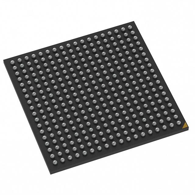


 工商网监
湘ICP备2023018690号
工商网监
湘ICP备2023018690号
