MLX80050KDC-BAA-000-TU 数据手册
MLX80050/51/30/31
LIN System Basis ICs
Datasheet
Features
VS
1
8
VCC
EN
2
7
NRES
MLX80030/50
LIN 2.x / SAE J2602 compliant
Operating voltage VSUP = 5 ... 27 V
3 modes: Normal, Silent and Sleep
Linear low drop voltage regulator:
GND
3
5
TxD
LIN
4
5
RxD
MLX80030/31:
Normal mode 3.3V/70mA ±2%
Silent mode 3.3V/20mA ±2%
MLX80050/51:
Normal mode 5V/70mA ±2%
Silent mode 5V/20mA ±2
Low current consumption (typ)
Sleep mode 20 A
Silent mode “noload” 45 A
Output current limitation
LIN-Bus Transceiver
Baud rate up to 20 kBaud
Slew rate control for best EME behaviour
Low slew mode for optimized SAE J2602 transmission
High impedance LIN pin in case of loss of ground or battery
Remote and local wake up source recognition
VCC undervoltage detection at NRES output (start-up delay 4ms)
Programmable Window Watchdog (only MLX80031/51)
VSUP undervoltage detection (POR), Over temperature shutdown
TxD dominant time out function, Standby mode time out after 350ms
Automotive temperature range of –40°C to 125°C
Interface I/O’s independent from voltage regulator output
Enhanced ESD robustness according to IEC 61000-4-2
Vres threshold 3.0 V (MLX80030/31); Vres threshold 4.1V (MLX80050/51)
Direct discharge for pin LIN >20kV (only Lin cap connected) and for pin VBAT >15kV
Indirect discharge for pin LIN >15kV
Load dump protected (40V)
Order Code
Temp. Range
Package
Delivery
Remark
MLX80050KDC-CAA-100-RE
MLX80051KLW-CAA-100-RE
MLX80030KDC-CAA-100-RE
MLX80031KLW-CAA-100-RE
-40 - 125 °C
-40 - 125 °C
-40 - 125 °C
-40 - 125 °C
SOIC8
QFN_WF20/5x5
SOIC8
QFN_WF20/5x5
Reel
Reel
Reel
Reel
Silent Mode enabled
Silent Mode enabled
Silent Mode enabled
Silent Mode enabled
Short Description
The MLX8005x/3x consist of a low-drop voltage regulator 5V/3.3V/70mA combined with a Reset/Watchdog unit and a LIN bus transceiver. The LIN transceiver is suitable for LIN bus systems conform to LIN specification revision 2.x and SAE J2602. The watchdog
times of the integrated window watchdog can be adapted on application needs via external resistors. With the help of an external
bipolar transistor it is possible to extend the output current of the integrated voltage regulator. The combination of voltage regulator
and bus transceiver as well as watchdog unit makes it possible to develop simple, but powerful and cheap slave nodes in LIN Bus
systems.
REVISION 13 – March 2020
3901080050
P a g e |1
�MLX80050/51/30/31
LIN System Basis ICs
Datasheet
Contents
1. LIST OF TABLES.................................................................................................................................. 4
2. LIST OF FIGURES ................................................................................................................................ 4
3. ELECTRICAL SPECIFICATION............................................................................................................... 5
3.1. DC CHARACTERISTICS ........................................................................................................................... 6
3.2. AC CHARACTERISTICS ......................................................................................................................... 11
3.3. TIMING DIAGRAMS ............................................................................................................................. 14
4. PIN CONFIGURATION ...................................................................................................................... 15
4.1. MLX80030 AND MLX80050 - SOIC8 ............................................................................................... 15
4.2. MLX80031 AND MLX80051 IN QFN20 ............................................................................................ 16
3. FUNCTIONAL DESCRIPTION ............................................................................................................. 17
3.1. SUPPLY PIN VS .................................................................................................................................. 19
3.2. EN INPUT PIN .................................................................................................................................... 19
3.3. GROUND PIN GND ............................................................................................................................ 19
3.4. LIN.................................................................................................................................................. 19
3.5. RECEIVER OUTPUT RXD ...................................................................................................................... 19
3.6. TRANSMIT INPUT TXD ........................................................................................................................ 19
3.6.1. TxD dominant time-out feature .......................................................................................... 19
3.7. OUTPUT NRES.................................................................................................................................. 20
3.8. VOLTAGE REGULATOR PINS VCC AND RTG ............................................................................................ 20
3.9. INH OUTPUT (ONLY MLX80031/51) ................................................................................................. 20
3.10. WAKE INPUT (ONLY MLX80031/51)............................................................................................... 20
3.11. KL15 INPUT (ONLY MLX80031/51) ................................................................................................. 20
3.12. WATCHDOG TRIGGER INPUT NWDI (ONLY MLX80031/51) ................................................................ 20
3.13. WATCHDOG OSCILLATOR RESISTOR RBWD (ONLY MLX80031/51) ........................................................ 20
3.14. MODE INPUT MODE (ONLY MLX80031/51) .................................................................................... 20
4. OPERATIONAL MODES .................................................................................................................... 21
4.1. MODES OVERVIEW ............................................................................................................................ 22
4.2. INITIALISATION AND STANDBY MODE ..................................................................................................... 23
4.3. NORMAL MODE ................................................................................................................................ 23
4.4. SILENT MODE.................................................................................................................................... 24
4.5. SLEEP MODE ..................................................................................................................................... 25
4.6. INIT-STATE........................................................................................................................................ 27
5. WAKE UP PROCEDURES................................................................................................................... 28
5.1. WAKE UP SOURCE RECOGNITION IN MLX80031/51 ............................................................................. 28
6. FUNCTIONALITY .............................................................................................................................. 29
6.1. RESET BEHAVIOUR OF MLX8003X/5X ................................................................................................ 29
6.2. THERMAL SHUTDOWN ........................................................................................................................ 29
6.3. VS UNDER VOLTAGE RESET .................................................................................................................. 29
6.4. LIN-TRANSCEIVER .............................................................................................................................. 30
REVISION 13 – March 2020
3901080050
P a g e |2
�MLX80050/51/30/31
LIN System Basis ICs
Datasheet
6.5. VOLTAGE REGULATOR ........................................................................................................................ 30
7. WINDOW-WATCHDOG (ONLY MLX80031/51) ................................................................................. 31
7.1. MLX80031/51 WATCHDOG BEHAVIOUR ............................................................................................ 31
7.2. ALL WATCHDOG START-UP SCENARIOS ................................................................................................... 32
7.2.1. After power-on and initialization ........................................................................................ 32
7.2.2. Wake up indicated transition to Standby Mode from Sleep or Silent Mode .................... 32
7.2.3. Undervoltage reset on VCC on Normal Mode or Silent Mode .......................................... 32
7.2.4. EN indicated transition from Silent Mode to Normal Mode.............................................. 32
7.3. CALCULATION OF WATCHDOG PERIOD .................................................................................................. 33
8. FAIL-SAFE FEATURES ....................................................................................................................... 35
9. APPLICATION HINTS ........................................................................................................................ 36
9.1. SAFE OPERATING AREA ....................................................................................................................... 36
9.2. APPLICATION CIRCUITRY ...................................................................................................................... 37
10. ESD AND EMC ............................................................................................................................... 38
10.1. RECOMMENDATIONS FOR ACTUATOR PRODUCTS .................................................................................. 38
10.1.1.
Automotive Qualification Test Pulses .......................................................................... 38
10.1.2.
Test Pulses On supply Lines ......................................................................................... 38
10.1.3.
Test pulses on Pin LIN ................................................................................................... 39
10.1.4.
Test pulses on signal lines ............................................................................................ 39
10.1.5.
EMV Test pulse definition ............................................................................................ 40
10.2. TYPICAL APPLICATION CIRCUITRY ........................................................................................................ 41
10.2.1.
External Circuitry on Supply Lines ............................................................................... 42
10.2.2.
External Circuitry on LIN Lines ..................................................................................... 42
10.2.3.
External Circuitry on Signal Lines ................................................................................. 42
11. MECHANICAL SPECIFICATION........................................................................................................ 43
11.1. SOIC8 PACKAGE.............................................................................................................................. 43
11.2. QFN20 5X5 PACKAGE ..................................................................................................................... 44
12. REVISION HISTORY ........................................................................................................................ 45
13. STANDARD INFORMATION REGARDING MANUFACTURABILITY OF MELEXIS PRODUCTS WITH
DIFFERENT SOLDERING PROCESSES .................................................................................................... 47
14. DISCLAIMER .................................................................................................................................. 48
15. CONTACT ...................................................................................................................................... 49
REVISION 13 – March 2020
3901080050
P a g e |3
�MLX80050/51/30/31
LIN System Basis ICs
Datasheet
1. List of Tables
TABLE 1: ABSOLUTE MAXIMUM RATINGS ........................................................................................................ 5
TABLE 2: VOLTAGE REGULATOR AND RESET UNIT ............................................................................................ 6
TABLE 3: LIN DC CHARACTERISTICS ............................................................................................................ 10
TABLE 4: AC CHARACTERISTICS ................................................................................................................... 11
TABLE 5: MLX80050/30 PIN LIST IN SOIC8 ............................................................................................... 15
TABLE 6: MLX80051/31 PIN LIST IN QFN20 .............................................................................................. 16
TABLE 7: MLX80050/30 OPERATION MODES ............................................................................................ 22
TABLE 8: MLX80051/31 OPERATION MODES ............................................................................................ 22
TABLE 9: PARAMETERS OF WINDOW WATCHDOG ......................................................................................... 34
TABLE 10: WINDOW WATCHDOG TIMING SELECTION .................................................................................... 34
TABLE 11: TEST PULSES SUPPLY LINE ........................................................................................................... 38
TABLE 12: TEST PULSES LIN ....................................................................................................................... 39
TABLE 13: TEST PULSES SIGNAL LINES ........................................................................................................... 39
TABLE 14: TEST PULSES SHAPES ISO7637-2 ................................................................................................ 40
TABLE 15: TEST PULSES SHAPES ISO7637-3 ................................................................................................ 41
TABLE 16: SOIC8 DIMENSIONS .................................................................................................................. 43
TABLE 17: QFN20 PACKAGE DIMENSIONS................................................................................................... 44
2. List of Figures
FIGURE 1: LIN PROPAGATION DELAYS .......................................................................................................... 14
FIGURE 2: LIN DUTY CYCLES ....................................................................................................................... 14
FIGURE 3: MLX80050/30 BLOCK DIAGRAM ............................................................................................... 17
FIGURE 4: MLX80051/31 BLOCK DIAGRAM ............................................................................................... 18
FIGURE 5: MLX8005X3X STATE DIAGRAM OF MODES OF OPERATION ............................................................... 21
FIGURE 6: LIN WAKE-UP FROM SILENT MODE ............................................................................................... 24
FIGURE 7 LOCAL WAKE-UP FROM SILENT MODE VIA WAKE ........................................................................... 25
FIGURE 8: REMOTE WAKE-UP FROM SLEEP MODE ......................................................................................... 26
FIGURE 9: LOCAL WAKE-UP FROM SLEEP MODE ............................................................................................ 27
FIGURE 10: VCC RESET BEHAVIOR ............................................................................................................... 29
FIGURE 11: MLX80031/51 WATCHDOG BEHAVIOR ..................................................................................... 31
FIGURE 12: WATCHDOG TIMING ................................................................................................................. 32
FIGURE 13: WATCHDOG OPEN AND CLOSE WINDOW TOLERANCES .................................................................... 33
FIGURE 14: SAFE OPERATING AREA FOR MLX80030/50 IN SOIC-8 FOR VSUP UP TO 18V ................................ 36
FIGURE 15: SAFE OPERATING AREA FOR MLX80031/51 IN QFN20 FOR VSUP UP TO 18V ................................ 36
FIGURE 16: APPLICATION CIRCUIT WITH MLX80050 OR MLX80030 (SLAVE NODE) ......................................... 37
FIGURE 17: APPLICATION CIRCUIT WITH MLX80031 OR MLX80051 (SLAVE NODE) ......................................... 37
FIGURE 18: SOIC8 DRAWING .................................................................................................................... 43
FIGURE 19: QFN20 DRAWING................................................................................................................... 44
REVISION 13 – March 2020
3901080050
P a g e |4
�MLX80050/51/30/31
LIN System Basis ICs
Datasheet
3. Electrical Specification
All voltages are referenced to ground (GND), positive currents flow into the IC.
Absolute Maximum Ratings
Parameter
Symbol
Condition
Min
Max
Unit
Respective to GND
-0.3
40
V
Transient voltage ISO 7637/2
pulse 1, 2
-100
100
V
Transient voltage ISO 7637/2
pulse 3A; 3B, coupling 1nF
-150
100
V
VLIN_DC
Respective to GND and VS
Loss of Ground (VGND =
VS)
-20
-30
40
40
V
VWAKE_DC
Respective to GND and VS
Loss of Ground (VGND =
VS)
-20
-30
40
40
V
Supply voltage at VS
VS
DC voltage LIN
DC voltage WAKE
DC voltage INH
VINH_DC
-0.3
VS+0.3
V
DC voltage VCC
VVCC_DC
-0.3
7
V
DC voltage RTG
VRTG_DC
-0.3
7
V
VIN
-0.3
7
V
Input voltage at low voltage I/O’s (EN, TxD,
RxD, NRES, WDI, RBWD, MODE)
VESDIEC
IEC 61000-4-2, direct ESD
Pin LIN with LIN cap 220pF
Pin VS to GND
VESDIECind
IEC 61000-4-2, indirect ESD
Pin LIN with LIN cap 220pF
VESDHBM
HBM (CDF-AEC-Q100-002)
Pin LIN
Pin WAKE, KL15, VS
Other pins
VESDCDM
CDM (AEC-Q100-011)
ESD voltage
20
15
kV
15
kV
±6
±4
±2
kV
kV
kV
±500
V
,
Power dissipation
Internal limited
see also chapter
9.1
P0
Thermal resistance from junction to ambient
RTHJA_SOIC8
JEDEC 1s0p board, no air
flow
150
K/W
RTHJA_QFN20
JEDEC 1s0p board, no air
flow
50
K/W
Junction temperature
TJ
-40
150
°C
Storage temperature
TSTG
-55
150
°C
Table 1: Absolute maximum ratings
REVISION 13 – March 2020
3901080050
P a g e |5
�MLX80050/51/30/31
LIN System Basis ICs
Datasheet
3.1. DC Characteristics
Unless otherwise specified all values in the following tables are valid for VS = 5 to 27V and
o
TAMB = -40 to 125 C. All voltages are referenced to ground (GND), positive currents flow into the IC.
For MLX80031/51 apply: RTG connected to VCC.
Table 2: Voltage Regulator and Reset Unit
Parameter
Symbol
Condition
Min
Typ
Max
Unit T[1]
Supply Voltage Pin VS
Nominal DC operating voltage
VS
5
27
V
A
1.01
VS under voltage reset
VSUVR_OFF
VS ramp up
4.1
5.0
V
A
1.02
VS under voltage reset
VSUVR_ON
VS ramp down
3.7
4.8
V
A
1.03
VS under voltage reset hysteresis
VSUVR_HYS
VSUVR_OFF - VSUVR_ON
0.04
0.3
0.7
V
A
VS 14V, VEN > 2V ,
LIN recessive, no load at
VCC
400
750
1500
A
A
Supply currents MLX80030, MLX80050
2.00
Supply current, normal mode
IVS_nor
VS 14V
2.01
Supply current, sleep mode
IVS_sleep
2.02
Supply current, silent mode
IVS_sil
TA = -40 °C
TA = 25 °C
TA 85 ° C
TA 125 °C
15
VS 14V, LIN recessive
no load at VCC
TA = -40 °C
TA = 25 °C
TA 85 ° C
TA 125 °C
65
30
20
30
45
85
95
100
125
A
A
A
A
Supply currents MLX80031, MLX80051
2.00
Supply current, normal mode
IVS_nor
VS 14V, VEN > 2V ,RBWD =
60k
LIN recessive, no load at
VCC
VS 14V
2.01
Supply current, sleep mode
IVS_sleep
2.02
Supply current, silent mode
IVS_sil
REVISION 13 – March 2020
3901080050
TA = -40 °C
TA = 25 °C
TA 85 ° C
TA 125 °C
VS 14V, LIN recessive
no load at VCC
TA = -40 °C
TA = 25 °C
TA 85 ° C
TA 125 °C
400
750
15
65
1500
30
20
30
45
85
95
100
125
P a g e |6
A
A
A
A
A
A
�MLX80050/51/30/31
LIN System Basis ICs
Datasheet
Voltage Regulator Pin VCC
MLX80050, MLX80051 (RTG connected to VCC)
3.01
Output voltage VCC
Output voltage VCC under
disturbances functional state A
3.02
3.03
Drop-out voltage [2]
3.04
3.05
Line regulation
3.06
3.07
Load regulation
3.08
VCCn5
6V VS 18V
1mA ILOAD 70mA
TA = 25°C
TA = -40°C to 125°C
4.90
4.85
5.0
5.10
5.15
V
A
5.25
V
C
VCCndis5
6V VS 18V, TA =
25°C
RLOAD = 330
VD10_5
VS 4V , IVCC = 10mA
75
120
mV
C
VD30_5
VS 4V , IVCC = 30mA
220
350
mV
C
VD70_5
VS 4V , IVCC = 70mA
500
800
mV
C
VLNR5
6V VS 18V, IVCC =
30mA
6V VS 18V, IVCC =
70mA
20
100
mV
A
VLDR10_5
1 mA < ILOAD < 10 mA
50
mV
A
VLDR30_5
1 mA < ILOAD < 30 mA
90
mV
A
VLDR70_5
1 mA < ILOAD < 70 mA
150
mV
A
-75
-80
mA
A
F
D
V
A
3.465
V
C
4.75
VS > 6V
3.09
Output current limitation [3]
3.10
Load capacity
IVCCLIM_5
TA = -40 °C
25 °C TA 125 °C
CLOAD
-135
-150
-110
2.2
22
3.234
3.201
3.3
MLX80030, MLX80031 (RTG connected to VCC)
3.01
Output voltage VCC
VCCn3
4 V VS 18 V
1m A ILOAD 70 mA
TA = 25 °C
TA = -40 °C to 125 °C
3.366
3.399
Output voltage VCC under
disturbances functional state
A
VCCndis3
6 V VS 18 V, TA =
25 °C
RLOAD = 330
Drop-out voltage [2]
VD10_3
VS 3 V , IVCC = 10 mA
100
mV
C
3.03
VD30_3
VS 3 V , IVCC = 30 mA
300
mV
C
3.04
VD70_3
VS 3 V , IVCC = 70 mA
700
mV
C
20
100
mV
A
3.02
3.135
3.05
Line regulation
VLNR_3
5 V VS 18 V, IVCC =
30mA
5V VS 18V, IVCC =
70mA
3.06
Load regulation
VLDR10_3
1 mA < ILOAD < 10 mA
50
mV
A
3.07
VLDR30_3
1 mA < ILOAD < 30 mA
90
mV
A
3.08
VLDR70_3
1 mA < ILOAD < 70 mA
150
mV
A
mA
A
3.09
Output current limitation [3]
REVISION 13 – March 2020
3901080050
IVCCLIM_3
VS > 4 V
TA = -40 °C
-135
-110
-75
P a g e |7
�MLX80050/51/30/31
LIN System Basis ICs
Datasheet
25 °C TA 125 °C
3.10
Load capacity
CLOAD
-150
-80
2.2
F
D
0.25
V
A
22
Output Pin NRES
4.01
Output voltage low
VOL_NRES
INRES = 1 mA
4.02
Leakage current low
Ileak_RxD
VNRES = 0 V
-5
5
µA
A
4.03
Leakage current high
Ileak_RxD
VNRES = VCC
-5
5
µA
A
Output voltage high NRES
under disturbances to fulfil
functional state A
VOH_NRES
Rload = 2.7 k to VCC
V
C
4.3
V
A
200
mV
C
3.15
V
A
VCC -1
MLX80050, MLX80051
5.01
VCC reset threshold on NRES
pin
VRES5V
5.02
VRES Hysteresis
VRESHYS = |VRES(ON) – VRES(OFF)|
VRESHYS5V
t > trr
3.9
4.10
MLX80030, MLX80031
5.01
VCC reset threshold on NRES
pin
VRES3V
5.02
VRES Hysteresis
VRESHYS = |VRES(ON) – VRES(OFF)|
VRESHYS3V
100
mV
C
0.8
V
A
V
A
t > trr
2.75
2.95
Input Pin EN
6.01
Input voltage low
VIL_EN
6.02
Input voltage high
VIH_EN
2.0
6.03
Hysteresis
VHYS_EN
50
100
700
mV
C
6.04
Pull-down resistor
Rpd_EN
50
125
250
k
A
V
A
VS-3.3V
V
A
-1
µA
A
VEN =VCC
Input Pin WAKE (MLX80031, MLX80051)
7.01
High level input voltage
VIH_WAKE
Sleep mode
VS-1V
7.02
Low level input voltage
VIL_WAKE
Sleep mode
7.03
Pull up current WAKE
IWAKE_PU
Normal & sleep
-30
7.04
Leakage current WAKE high
IWAKE_lk
VS = 18V
-5
5
µA
A
-15
Input Pin KL15 (MLX80031, MLX80051)
8.01
High level input voltage
VIH_KL15
Rv = 50k
4
VS+0.3V
V
A
8.02
Low level input voltage
VIL_KL15
Rv = 50k
-1
2
V
A
8.03
Pull down current KL15
IKL15_PD
65
µA
A
0.8
V
A
V
A
30
Input Pin MODE (MLX80031, MLX80051)
23.01
Input voltage low
VIL_MODE
23.02
Input voltage high
VIH_MODE
REVISION 13 – March 2020
3901080050
2.0
P a g e |8
�MLX80050/51/30/31
LIN System Basis ICs
Datasheet
23.03
Hysteresis
VHYS_MODE
23.04
Pull-down resistor
Rpd_MODE
50
VMODE = VCC
100
200
600
mV
C
600
k
A
0.8
V
A
V
A
Input Pin NWDI (MLX80031, MLX80051)
9.01
Input voltage low
VIL_NWDI
9.02
Input voltage high
VIH_NWDI
2.0
9.03
Hysteresis
VHYS_NWDI
50
100
600
mV
C
9.04
Pull-up resistor to VCC
Rpu_NWDI
125
250
375
k
A
9.05
Min low pulse width
1
D
V
A
VNWDI = 0V
Tminlow_NWDI one WD_OSC clock period
1
Watchdog Oscillator pin RBWD (MLX80031, MLX80051)
10.01
Voltage at RBWD
VRBwd
10.02
Range of RBWD resistance
RBWD
10.03
RBWD short resistance threshold to enable fail-safe state
IOUT = -50 A
1.2
20
60
k
B
0
330
B
60
A
RBWDSH
see paragraph 7.3
RON_INH
VS = 12V
IleakH_INH
Sleep Mode, VINH = 18V,
VS = 18V
-5
5
µA
A
IleakL_INH
Sleep Mode, VINH = 0V,
VS = 18V
-5
5
µA
A
170
190
°C
D
10
30
°C
D
Output INH (MLX80031, MLX80051)
11.01
ON Resistance
11.02
Leakage current INH high
11.03
Leakage current INH low
20
Thermal Protection
Thermal shutdown
TJSHD
Thermal hysteresis
TJHYS
155
Notes:
[1]
A = 100% serial test, B = Operating parameter, C = characterization data,
D = Value guaranteed by design
[2]
The nominal VCC voltage is measured at VSUP = 12V. If the VCC voltage is 100mV below its nominal value then the voltage drop is VD =
VSUP – VCC
[3]
Functionality range of current limitation at silent mode is limited by reset threshold VRES. Below them the IC change to normal mode.
Validity for IVCC_MAXsil: VCCn (min) ≤ VCC ≤ VRES
REVISION 13 – March 2020
3901080050
P a g e |9
�MLX80050/51/30/31
LIN System Basis ICs
Datasheet
Table 3: LIN DC Characteristics
Parameter
Symbol
Condition
Min
Typ
Max
Unit
T[1]
80
A
A
60
k
A
µA
A
General
12.01
Pull up current LIN (recessive)
IINLINpu
VLIN = 18 V, VS = 6V
12.02
Pull up resistor LIN
RLINpu
VS = 12V, VLIN = 0V
20
12.03
Reverse current LIN
(dominant)
IINLINdom
VS = 12V, VLIN = 0V
-400
12.04
Reverse current LIN
(recessive)
IINLINrec
VLIN VS, 8V VLIN
18V,
8V VS 18V
0
23
µA
A
12.05
Reverse current LIN
(loss of battery)
IINLIN_lob
VS = 0V, 0V VLIN
18V
0
23
µA
A
12.06
Reverse current LIN
(loss of ground)
IINLIN_log
VS= 12V, 0V VLIN
18V
-10
50
µA
A
Voltage drop serial Diode
VSerDiode
1.0
V
D
Battery Shift
VShift_BAT
related to VS
0
11.5
%
D
Ground Shift
VShift_GND
related to VS
0
11.5
%
D
Ground-Battery shift difference
VShift_diff
related to VS
0
8
%
D
0.4
30
0.7
Receiver
Receiver dominant voltage
VBUSdom
Receiver recessive voltage
VBUSrec
12.08
Centre point of receiver
threshold Vthr_cnt =
(Vthr_rec+Vthr_dom)/2
Vthr_cnt
12.09
Receiver Hysteresis
Vhys = Vthr_rec-Vthr_dom
12.07
0.4*VS
A
0.6*VS
7.0 V VS 18 V
0.475*VS
Vhys
A
V
0.5*VS
0.525*VS
A
0.15*VS
0.175*VS
A
D
Transmitter
12.10
Transmitter dominant voltage
12.11
Current limitation LIN
12.12
Transmitter recessive voltage
Rload = 500, VS = 5V
0
1.2
Rload = 500, VS >=
7V
0
0.2*VS
ILIM
VLIN = VS, TxD = 0V
40
VohBUS
No load, VEN = 0/5V,
VTxD = 5V
0.8*VS
rising
VoIbus
120
V
A
200
mA
A
VS
V
A
0.8
V
A
V
A
700
mV
C
375
k
A
Input/Output Pin TxD
13.01
Input voltage low TxD
VIL_TxD
13.02
Input voltage high TxD
VIH_TxD
2
13.03
Hysteresis
VHYS_TxD
50
13.04
Pull-up resistor to VCC
Rpu_TxD
REVISION 13 – March 2020
3901080050
VTxD = 0V
125
250
P a g e | 10
�MLX80050/51/30/31
LIN System Basis ICs
Datasheet
13.06
Low level output current
IOL_TxD
local wake-up request;
standby mode;
VTxD = 0.4V
1.5
mA
A
0.6
V
A
7
k
A
5
µA
A
V
C
Output Pin RxD
14.01
Output voltage low RxD
VOL_RxD
IRxD = 2 mA
14.02
Pull-up resistor to VCC
Rpu_RxD
VRxD = 0V
3
14.03
Leakage current high
Ileak_RxD
VRxD = VCC
-5
Output voltage high RxD
under disturbances to fulfil
functional state A
VOH_RxD
Rload = 2.7k to VCC
5
VCC -1
Notes:
[1]
A = 100% serial test, B = Operating parameter, C = characterization data,
D = Value guaranteed by design
3.2. AC Characteristics
6V VS 27V, -40°C TA 125°C, RTG connected to VCC, unless otherwise specified
Table 4: AC Characteristics
Parameter
Symbol
Condition
Min
Typ
Max
Unit
T
[1]
Reset parameter on NRES
16.01
Reset time
16.02
Reset rising time
tRes
VS = 14V
2.5
4
5.5
ms
A
trr
VS = 14V
3.0
6.5
12
s
A
tWDOSC20
RBWD = 20k1%
7.0
8.05
9.0
s
A
tWDOSC60
RBWD = 60k1%
19.0
23.05
25.2
s
A
Watchdog parameter on NRES (MLX80031, MLX80051)
17.01
17.02
Watchdog-Oscillator Period
Watchdog Close Window
Watchdog Open Window
17.05
Watchdog Reset Low Time
Watchdog Lead Window
17.06
Watchdog Safety Oscillator
REVISION 13 – March 2020
3901080050
tCW
tCW = cycles *
tWDOSC
1053
cycles
D
tOW
tOW = cycles *
tWDOSC
1105
cycles
D
ms
A
cycles
D
µs
A
tWDres
tLDT
tWDsafety
3
tOWS = cycles *
tWDOSC
RBWD open /
RBWD gnd
4
5
7895
30
50
75
P a g e | 11
�MLX80050/51/30/31
LIN System Basis ICs
Datasheet
Wake-up and Mode Control
150
s
A
50
s
A
168
250
s
A
5
15
20
s
A
VEN = 5V
5
15
20
s
A
tpd_sil_n
VEN = 5V
Silicon Revision C
5
15
40
s
A
tpd_sil
check falling edge
on RBwd, EN = 0V
Silicon Revision C
20
s
A
18.01
Remote Wake-up filter time
twu_remote
30
18.02
Wake-up filter time on WAKE
(only MLX80051,MLX80031)
twu_WAKE
Sleep or Silent
Mode,
WAKE falling edge
10
18.03
Wake-up filter time on KL15
(only MLX80051,MLX80031)
twu_KL15
Sleep or Silent
Mode,
KL15 rising edge
80
18.04
Propagation delay from Normal
Mode to Sleep Mode via EN
tpd_sleep
VEN = 0V
18.05
Propagation delay from Standby
Mode to Normal Mode via EN
tpd_norm
18.06
Propagation delay from Silent
Mode to Normal Mode via EN
18.07
Propagation delay: go to
silent mode after EN=H/L
70
Setup time TxD to EN for low
slew mode
tset_TxD_EN
5
s
B
Hold time TxD after EN for low
slew mode
thold_TxD_EN
20
s
B
TXD hold time for mode change
thold_TxD_MCH
2
s
D
20
s
A
18.08
Debouncing time EN
tdeb_EN
2
18.09
TxD dominant time out
tTxD_to
Normal Mode,
VTxD = 0V
27
60
ms
A
18.10
Standby time out
tsby_to
Standby Mode,
VEN= 0V
150
500
ms
A
18.11
Wake up time vs. EN
twu_EN
Wake form sleep
via EN=L/H
20
s
A
tdr_RxD
tdf_RxD
CL(RXD) = 50 pF
6
s
A
tdsym_RxD
tdr_RXD - tdf_RXD
2
s
A
4.0
s
D
2
5
5
General LIN Parameter
19.01
Receiver propagation delay
LIN -> RxD
19.02
Symmetry prop. delay LIN->RxD
19.03
Receiver debouncing time
REVISION 13 – March 2020
3901080050
tdeb_LIN
-2
1.5
2.8
P a g e | 12
�MLX80050/51/30/31
LIN System Basis ICs
Datasheet
19.04
slew rate rising edge LIN
dV/dTrise
19.05
slew rate falling edge LIN
dV/dTfall
19.06
slew rate rising edge LIN
dV/dTrise
19.07
slew rate falling edge LIN
dV/dTfall
Internal capacity
CLIN
Normal Mode
LIN-Load: 1kΩ/1nF
Low Slew Mode
LIN-Load: 1kΩ/1nF
1.0
1.5
2.5
V/s
C
-2.5
-1.5
-1.0
V/s
C
0.3
0.8
1.3
V/s
C
-1.3
-0.8
-0.3
V/s
C
25
35
pF
D
Pulse at LIN via
10kOhm with 0/10V;
VS = open
LIN transceiver parameter according to LIN Physical Layer Spec. rev. 2.0, table 3.4 (20kbit/s)
Conditions:
Normal slew mode; VS =7.0V to 18V; LIN loads: 1k/1nF; 660/6.8nF; 500/10nF
TxD signal: tBit = 50µs, twH = TwL = tBit; trise = tfall < 100ns
Minimal recessive bit time
trec(min)
40
50
58
s
Maximum recessive bit time
trec(max)
40
50
58
s
20.01
Duty cycle 1
D1
D1 = trec(min) / (2*tBit)
20.02
Duty cycle 2
D2
D2 = trec(max) / (2*tBit)
0.396
A
0.581
A
Transceiver parameter according to LIN Physical Layer Spec. rev. 2.0, table 3.4 (10.4kbit/s)
Conditions:
Low slew mode; VS =7.0V to 18V; LIN loads: 1k/1nF; 660/6.8nF; 500/10nF
TxD signal: tBit = 96µs, twH = TwL = tBit; trise = tfall < 100ns
Minimal recessive bit time
trec(min)
80
96
113
s
Maximum recessive bit time
trec(max)
80
96
113
s
21.01
Duty cycle 1
D3
D3 = trec(min) / (2*tBit)
21.02
Duty cycle 2
D4
D4 = trec(max) / (2*tBit)
0.417
A
0.590
A
LIN transceiver parameter according to SAE J2602 (10.4kbit/s)
Conditions:
Low slew mode; VS =7.0V to 18V; LIN loads: 1k/1nF;660/6.8nF;500/10nF
TxD signal: tBit = 96µs, twH = TwL = tBit; trise = tfall < 100ns
22.01
Minimal recessive delay
TxD -> LIN
tx_rec_min
48
s
A
22.02
Maximum recessive delay
TxD -> LIN
tx_rec_max
48
s
A
22.03
Minimal dominant delay
TxD -> LIN
tx_dom_min
48
s
A
22.04
Maximum dominant delay
TxD -> LIN
tx_dom_max
48
s
A
22.05
Maximum rec. to dom. delay
Tr_d_max
tx_rec_max - tx_dom_min
15.9
s
A
22.06
Maximum dom. to rec. delay
Td_r_max
tx_dom_max - tx_rec_min
17.2
s
A
Notes:
[1]
A = 100% serial test, B = Operating parameter, C = characterization data,
D = Value guaranteed by design
REVISION 13 – March 2020
3901080050
P a g e | 13
�MLX80050/51/30/31
LIN System Basis ICs
Datasheet
3.3. Timing diagrams
50%
TxD
tdf_TXD
tdr_TXD
VBUS
100%
95%
LIN
50%
50%
5%
0%
tdr_RXD
tdf_RXD
RxD
50%
transceiver_delays.vsd
Figure 1: LIN propagation delays
tBit
tBit
TxD
tx_rec_max
tx_dom_max
tx_dom_min
VSUP
trec(min)
tx_rec_min
100%
tdom(max)
74.4%
(77.8%)
tdom(min)
LIN
58.1%
(61.6%)
Level for LSM in brackets
28.4%
(25.1%)
VSS
58.1%
(61.6%)
42.2%
(38.9%)
trec(max)
28.4%
(25.1%)
0%
timing_lin20.vsd
Figure 2: LIN duty cycles
REVISION 13 – March 2020
3901080050
P a g e | 14
�MLX80050/51/30/31
LIN System Basis ICs
Datasheet
4. Pin Configuration
4.1. MLX80030 and MLX80050 - SOIC8
VS
1
8
VCC
EN
2
7
NRES
MLX80030/50
Pin
GND
3
5
TxD
LIN
4
5
RxD
Name IO-Typ
Description
1
VS
P
Battery supply voltage
2
EN
I
Mode control pin, enables the normal operation mode when HIGH
3
GND
G
Ground
4
LIN
I/O
LIN bus transmitter/receiver pin,
(low = dominant)
5
RxD
I/O
Received data from LIN bus, low in dominant state; internal pull-up resistor
6
TxD
I/O
Transmit data input (low = dominant)
7
NRES
O
Undervoltage reset output (open drain),
low active
8
VCC
P
Voltage regulator output
Table 5: MLX80050/30 pin list in SOIC8
REVISION 13 – March 2020
3901080050
P a g e | 15
�MLX80050/51/30/31
LIN System Basis ICs
Datasheet
4.2. MLX80031 and MLX80051 in QFN20
Pin
Name
IO-Typ
Description
1
EN
I
2
NC
3
NWDI
I
Watchdog trigger input; negative edge; pull-up
4
WAKE
I
High voltage input for local wake up, negative edge triggered
5
GND
G
Ground
6
NC
7
LIN
8
NC
9
RxD
I/O
10
INH
O
11
TxD
I/O
Transmit data input (low = dominant)
12
NRES
O
Reset output (open drain), low active
13
RBWD
I/O
Bias resistor for watchdog oscillator
14
NC
15
MODE
I
Input to control window watchdog
16
KL15
I
High voltage input for local wake up, positive edge triggered
17
NC
18
VCC
I
Voltage regulator sense input
19
RTG
P
Voltage regulator output
20
VS
P
Battery supply voltage
EP
G
Exposed pad should be connected to Ground
Mode control pin, enables the normal
operation mode when HIGH
not connected
not connected
I/O
LIN bus transmitter/receiver pin,
(low = dominant)
not connected
Received data from LIN bus, low in dominant state; internal pull-up resistor
High side switch; High voltage
not connected
not connected
Table 6: MLX80051/31 pin list in QFN20
REVISION 13 – March 2020
3901080050
P a g e | 16
�MLX80050/51/30/31
LIN System Basis ICs
Datasheet
3. Functional Description
The MLX8003x/5x consists of a low drop 3.3V/5V voltage regulator capable to drive 70mA and a LIN bus transceiver,
which is a bi-directional bus interface for data transfer between LIN bus and the LIN protocol controller. Additionally
integrated is a Window-Watchdog/RESET unit with a fixed power-on-reset delay of 4 ms and an adjustable watchdog
time defined by an external bias resistor.
VS
VCC
control
amplifier
Aux.
Supply
3
5
VBG
POR
4.1 V /
2.9V
Temp.
Protection
Adjust
ment
VS
TSHD
Undervoltage
Reset
UVR
Mode
Control
EN
Reset
Generator
VBG
SBY
6bit Reg Calib
ZZ 16bit
4bit
BG
BG
current
limitation
Standby
timer
350k
Reset
PORTimer
RESETBuffer
NRES
fosc
RC
osc.
VSS
VCC
Wake-Filter
Receiver
VSUP
5k
70s
Vaux
RxDBuffer
RxD
Rec-Filter
30k
VCC
Transmitter
LIN
SBY
Driver
control
250k
TxDTimeout
TxD
POR
Figure 3: MLX80050/30 Block Diagram
REVISION 13 – March 2020
3901080050
P a g e | 17
�MLX80050/51/30/31
LIN System Basis ICs
Datasheet
VS
RTG
Vaux
control
amplifier
Aux.
Supply
VBG
VBG
BG
VCC
Reset
Generator
Vaux
Vaux
5
Adjust
ment
POR
4.1 V /
2.9V
Vaux
POR
TSHD
SBY
6bit Reg Calib
ZZ 16bit
4bit
BG
3
current
limitation
5V / 3.3V
VSUP
TSHD
RC
osc.
Undervoltage
Reset
POR
UVR
Standby
timer
Test logic
TxDTimeout
timer
EN
INH
fosc
Reset
PORTimer
RESETBuffer
NRES
Window
watchdog
Mode
Control
350k
VS
91kHz
SBY
ZZ
Control
Vaux
VCC
VS
RxDcontrol
Wake_sig
fwdosc
WD
Osc
VBG
WAKE
RBWD
VCC
250k
KL15_sig
WDI_sig
KL15
70s
MODE
TxD_out
Receiver
VS
Wake-Filter
to_RxD
Vaux
Vaux
250k
VCC
RecFilter
30k
5k
RxD_out
Transmitter
LIN
VSS
NWDI
SBY
Driver
control
RxDBuffer
RxD
VCC
250k
UVR_POR
TxD
VSS
Figure 4: MLX80051/31 Block Diagram
REVISION 13 – March 2020
3901080050
P a g e | 18
�MLX80050/51/30/31
LIN System Basis ICs
Datasheet
3.1. Supply Pin VS
VS is the operational voltage pin of MLX8005x/3x. The voltage range is VS = 6 to 18V. After switching on VS, the
MLX8003x/5x starts at Standby Mode and the VCC voltage regulator ramps up. An undervoltage detection unit prevent
an undefined operation for Vs < 4V.
VS- Power-ON
If VS is switched on, the MLX8003x/5x starts in Standby Mode. A combination of dynamic POR and under voltage reset
circuitry generates a POR signal, which switches the MLX8003x/5x on. This power on behaviour is independent from the
status of the EN-pin.
Power-on reset and under-voltage reset operate independent from each other, which secures the independence from
the rise time of VS.
3.2. EN input pin
The ENable input is the mode control pin of MLX8003x/5x in combination with the TxD input.
The MLX8003x/5x is switched into the Sleep Mode with a falling edge and into normal mode with a rising edge at the
EN pin. The state machine goes to Normal Mode after t Res (see also Table 4: AC Characteristics). The Normal Mode will
be kept as long as EN remains high.
The Normal Mode can be entered from Standby Mode, when the pin EN is driven HIGH. To prevent unwanted mode
transitions, the EN input contains a debounce filter as specified (tEN_deb).
The pin EN contains a weak pull down resistor. The input thresholds are compatible to 3.3V and 5V supply systems.
MLX80031/51:
Additionally the positive edge on pin EN results in an immediate reset of the active low interrupt on pin RxD as well as
the wake-up source recognition flag on pin TxD.
3.3. Ground pin GND
This is the reference pin of the IC. The absence of GND connection will not influence or disturb the communication between other LIN bus nodes.
3.4. LIN
This bidirectional pin consists of a low side driver in the output path and a high-voltage comparator in the input path.
Furthermore is integrated a LIN pull-up resistor between LIN and VS pin. Low side driver consist a current limitation.
3.5. Receiver Output RxD
The pin RxD is a buffered open drain output. Output signals can be shifted by the external pull up resistor to 3.3V and
5V supply systems.
3.6. Transmit Input TxD
The transmit data stream of the LIN protocol controller applied to the pin TxD is converted into the LIN bus signal with
slew rate control in order to minimize electromagnetic emissions.
The pin TxD contains a weak pull up resistor. The input thresholds are compatible to 3.3V and 5V supply systems. To
enable the transmit path, the TxD pin has to be driven recessive (HIGH) after or during the normal mode has been entered.
3.6.1. TxD dominant time-out feature
With the first dominant level on pin TxD after the transmit path has been enabled, the dominant time-out counter is
started. In case of a faulty blocked permanent dominant level on pin TxD the transmit path will be disabled after the
specified time tTxD_to. The time-out counter is reset by the first negative edge on pin TxD.
REVISION 13 – March 2020
3901080050
P a g e | 19
�MLX80050/51/30/31
LIN System Basis ICs
Datasheet
3.7. Output NRES
The NRES pin outputs the reset state as well as the watchdog condition in MLX80031 and MLX80051.
3.8. Voltage regulator pins VCC and RTG
The MLX80030/50 has an integrated low drop linear regulator with a p-channel-MOSFET as driving transistor. This regulator outputs a voltage of 5V ±2% (MLX80050/51) or 3.3V ±2% (MLX80030/31) with a load current of max. 70mA. The
current limitation unit limits the output current for short circuits or overload to 130mA by decreasing the VCC voltage.
This way the power dissipation is held constant at a maximum value.
The voltage regulator has two pins, output pin RTG and sense input pin VCC. For MLX80030/50 both, RTG and VCC, are
commonly bonded to pin VCC on the package.
Devices MLX80031/51 has both pins bonded and provides the possibility to use an external npn transistor to boost the
maximum load current. In this case the basis of the npn transistor has to be connected to the RTG pin and the emitter
to the VCC pin. In case of using the internal voltage regulator, both pins have to be connected to each other.
3.9. INH Output (only MLX80031/51)
INH switches to high (VS connected to INH) in case of Standby or Normal Mode. INH is switched off at Silent and Sleep
Mode. The pin will be used for switch on an external power supply or for switch off the external 1k master resistor in
master node applications.
3.10. WAKE Input (only MLX80031/51)
High voltage input pin for local wake-up functionality. With a falling edge on WAKE the IC wakes-up from Silent Mode
or Sleep Mode to Standby Mode.
The pin WAKE provides a weak pull up current source towards Vs which provides a HIGH level on the pin in case of open
circuit failures or if no local wake-up feature is required. In such applications it is recommended to connect the pin
WAKE directly to pin Vs in order to prevent influences due to EMI.
3.11. KL15 Input (only MLX80031/51)
High voltage input pin for local wake-up functionality. With a rising edge on KL15 the IC wakes-up from Silent Mode or
Sleep Mode to Standby Mode.
The pin KL15 provides a weak current sink towards GND which provides a LOW level on the pin in case of open circuit
failures or if no local wake-up feature is required. In such applications it is recommended to connect the pin KL15 directly to GND in order to prevent influences due to EMI. KL15 is typically connected to the ignition terminal and generates a local wake-up at start of ignition.
3.12. Watchdog Trigger Input NWDI (only MLX80031/51)
This input is used to trigger the integrated window watchdog in MLX80031/51. Every falling edge on NWDI in watchdog
open window is used to reset the watchdog timer. An internal pull up resistor of 250k secures a stable high condition if
this pin is open. The NWDI input is a low voltage CMOS input. The minimum low time of NWDI is one WD_OSC clock
period to allow falling edge detection.
3.13. Watchdog Oscillator Resistor RBWD (only MLX80031/51)
A resistor between RBWD and GND defines the window watchdog times as trigger time.
3.14. Mode Input MODE (only MLX80031/51)
Special pin for to disable the window watchdog function. For normal watchdog operation connect the MODE pin to
GND directly or via external resistor. With MODE pin on 3.3V/5V the window watchdog is switched off.
REVISION 13 – March 2020
3901080050
P a g e | 20
�MLX80050/51/30/31
LIN System Basis ICs
Datasheet
4. Operational Modes
The MLX8003x/5x provides four main operating modes “Standby”, “Normal”, “Silent” and “Sleep”. The main modes are
fixed states defined by basic actions (VS start, EN or wake-up).
Start Vaux;
Regulator OFF
VSUP power on
Regulator on; VCC ramp up
VCC cross reset threshold -> start tres
LIN transmitter off
LIN termination 30k
--------------------------------------------------after power on:
RxD: high
TxD: high
after wake up:
RxD: low
TxD: wake source output
--------------------------------------------------No lead timer / closed WD window
Init
End of Initialization
Standby
Local wake-up or
Remote wake-up
or EN = L/H
Local wake-up or
Remote wake-up or
Vcc < VRES
Vcc < VRES
SleepMode
EN = H[2] or L/H [1]
t > tsby (350ms) &
Vcc > VRES
EN = H/L & TxD =H
Silent
Mode
EN = H/L & TxD=L
EN = L/H
Regulator off
LIN transmitter off
LIN termination 200k
----------------------------------------------RxD: floating (0V)
TxD: floating (0V)
--------------------------------------------------No lead timer / closed WD window
Regulator on
LIN transmitter off
LIN termination 30k
-----------------------------------------RxD = high
TxD = high
--------------------------------------------------No lead timer / closed WD window
Normal
Mode
Regulator on
NRES = H
LIN transmitter on
LIN termination 30k
-----------------------------------------------RxD:= data output
TxD:= data input
[1] Set Slew Mode:
Normal => EN=L/H & TxD=H (default)
Low Slew => EN=L/H & TxD=L
[2] Only after Wake-up from Sleep mode
with EN=L/H
Figure 5: MLX8005x3x state diagram of modes of operation
REVISION 13 – March 2020
3901080050
P a g e | 21
�MLX80050/51/30/31
LIN System Basis ICs
Datasheet
4.1. Modes Overview
Mode
VCC
TxD
RxD
LIN
remarks
Standby
3.3V/5V
high
high
recessive
entered after power on
or wake up
Normal
3.3V/5V
input for
transmit data
stream
output for LIN data stream
follows TxD
[1]
Silent
3.3V/5V
high
high
recessive
high = 3.3V/5V
recessive
remote wake up to
enter Standby Mode,
EN = H to go to Normal
Mode
Sleep
0
floating
floating
Table 7: MLX80050/30 Operation Modes
[1]
Normal mode will be entered form Standby Mode by a low -> high transition on pin EN and from Sleep Mode by EN = H after startup of the
regulator. When recessive level (high) on pin TxD is present the transmit path will be enabled
Mode
VCC
TxD
RxD
LIN
INH
Watchdog
remarks
Standby
3.3V/5V
High/ active
[1]
low
high/
[2]
active low
recessive
ON
ON
entered after
power on or wake
up
Normal
3.3V/5V
input for
transmit data
stream
output for
LIN data
stream
follows TxD
ON
ON
Silent
3.3V/5V
high
high
recessive
OFF
OFF
Sleep
0
floating
floating
recessive
OFF
OFF
[3] [4] [5]
Local or remote
wake up to enter
Standby Mode,
EN = H to go to
Normal Mode
Table 8: MLX80051/31 Operation Modes
[1]
[2]
[3]
[4]
[5]
Indicates the wake up flag in case of local wake up
After power on RxD is going high via pull-up to Vcc. If any wake up(local or remote) occurs it will be indicated by active low
Active low interrupt at pin RxD will be removed when entering normal mode
Wake up source flag at pin TxD will be removed when entering normal mode
Normal mode will be entered from Standby Mode by a low -> high transition on pin EN and from Sleep Mode by EN = H after startup of the
regulator. When recessive level (high) on pin TxD is present the transmit path will be enabled
REVISION 13 – March 2020
3901080050
P a g e | 22
�MLX80050/51/30/31
LIN System Basis ICs
Datasheet
4.2. Initialisation and Standby mode
When the battery supply voltage VS exceeds the specified threshold V SUVR_OFF, the MLX8003x/5x automatically enters
the Standby Mode. Following internal procedure is running:
First:
Start of internal supply Vaux and POR of Vaux
Start of internal RC oscillator
Second and parallel after POR:
Start of voltage regulator
The output voltage VCC ramps up to nominal value. The pin RxD is floating and the integrated slave pull up resistor with
decoupling diode pulls the pin LIN. The transmitter as well as the receiver is disabled.
If there occurs no mode change to Normal Mode via an EN LOW to HIGH transition within the time stated (typically
350ms), the IC enters the most power saving Sleep Mode.
Furthermore the standby mode will be entered after a valid local or remote wake up event, when the MLX8003x/5x is
in Sleep or Silent mode. The entering of the standby mode after wake up will be indicated by an active LOW interrupt
on pin RxD.
4.3. Normal Mode
This mode is the base mode. The bus transceiver is able to send with a max baud rate of 20kbit/s.
The whole MLX8003x/5x is active. The incoming bus traffic is detected by the receiver and transferred via the RxD output pin to the microcontroller.
Exit the Normal Mode with one of the following conditions:
1. High-to-low edge on EN pin with TxD = H -> switch to Silent Mode
2. High-to-low edge on EN pin with TxD = L -> switch to Sleep Mode
3. Undervoltage monitor on VCC detects a low voltage reset condition (VCC < V RES) -> switch back to stand-by
mode.
Low Slew Mode
The first rising edge on EN after power-on defines the slew rate of the device. With TxD = High at this point works the
MLX8003x/5x with normal slew rate (default state). TxD = Low activates the Low Slew Mode, as long as VS > V SUVR_OFF.
In this mode the slew rate is switched from the normal value of typ. 1.6V/µs to a low value of typ. 0.8V/µs. This mode is
optimized to send with a maximum baud rate of 10.4kbit/s (acc. to SAE J2602). Because of this reduction of the slew
rate the EME behaviour is improved especially in the frequency range of 100 kHz to 10MHz.
REVISION 13 – March 2020
3901080050
P a g e | 23
�MLX80050/51/30/31
LIN System Basis ICs
Datasheet
4.4. Silent Mode
The Silent Mode is a special mode for application with active Sleep Mode on LIN, but the connected MCU still needs to
be supplied with VCC.
With a falling edge on EN input in combination with TxD=high switches the MLX8003x/5x from Normal Mode to the
Silent Mode with reduced internal current consumption.
In Silent Mode the voltage regulator is on with a 2% tolerance. The transmitter is disabled and the pin RxD is disconnected from the receive path and is floating. The slave termination resistor (LIN pull up resistor with decoupling diode
between pins LIN and VS) is disconnected; only a weak current source is applied to the LIN bus. Value is typical -75uA,
limits -20…-100uA.
Exit the silent mode with one of the following conditions:
1. Low-to-high edge on the EN pin -> switch back to normal mode
2. Remote wake up (all versions) or local wake up request (MLX80031/51 only) -> switch to standby mode
3. Undervoltage monitor on VCC detects a low voltage reset condition (VCC < VRES) -> switch back to stand-by
mode.
Normal Mode
Silent Mode
Standby Mode
Normal Mode
EN
tpd_sil
TxD
VCC
Regulator ON
twu_remote
Transmitter ON
LIN
RxD
Transmitter ON
Transmitter OFF
Low
NRES
Watchdog *
Watchdog ON
Watchdog OFF
Start watchdog lead time
* only for MLX80031/51
timing_silent_mode.vsd
Figure 6: LIN wake-up from Silent Mode
REVISION 13 – March 2020
3901080050
P a g e | 24
�MLX80050/51/30/31
LIN System Basis ICs
Datasheet
Normal Mode
Silent Mode
Standby Mode
Normal Mode
EN
tpd_sil
TxD
low *
VCC
Regulator ON
twu_WAKE
WAKE *
LIN
Transmitter ON
RxD
low
Undervoltage detection active
NRES
Watchdog *
Transmitter ON
Transmitter OFF
Watchdog ON
Watchdog OFF
Start watchdog lead time
* only for MLX80031/51
timing_sleep_mode_locwu.vsd
Figure 7 Local Wake-up from Silent Mode via WAKE
4.5. Sleep Mode
The most power saving mode of the MLX8003x/5x is the Sleep Mode. The MLX8003x/5x offers two procedures to enter
the sleep mode:
The mode is selected from normal mode with a falling edge on EN in combination with
TxD = L.
If the MLX8003x/5x is in Standby Mode after power-on or wake-up, a sleep counter is started and switches the
transceiver into Sleep Mode after the specified time (typ. 350ms) even when the microcontroller of the ECU
will not confirm the normal operation by setting the EN pin to logic HIGH. This new feature allows faulty
blocked LIN nodes to reach always the most power saving mode.
Being in Sleep Mode the voltage regulator switched off in order to minimize the current consumption of the complete
LIN node. The transmitter is disabled and the pin RxD is disconnected from the receive path and is low (follows VCC).
The slave termination resistor (LIN pull up resistor with decoupling diode between pins LIN and VS) is disconnected,
only a weak current source is applied to the LIN bus (see chapter 8 fail-safe features)
Exit the Sleep Mode with the following condition:
1. Remote (all versions) or local wake up request (MLX80031/51 only) -> Switch to Standby Mode
2. EN = L/H -> Switch to Standby Mode
REVISION 13 – March 2020
3901080050
P a g e | 25
�MLX80050/51/30/31
LIN System Basis ICs
Datasheet
Figure 8: Remote wake-up from Sleep Mode
REVISION 13 – March 2020
3901080050
P a g e | 26
�MLX80050/51/30/31
LIN System Basis ICs
Datasheet
Normal Mode
Sleep Mode
Standby Mode
Normal Mode
EN
TxD
low *
VCC
tpd_sleep
twu_WAKE
WAKE *
LIN
Transmitter ON
RxD
Transmitter ON
Transmitter OFF
floating
low
Reset time
NRES
Watchdog *
Watchdog ON
Watchdog OFF
* only for MLX80031/51
Start watchdog lead time
timing_sleep_mode_locwu.vsd
Figure 9: Local wake-up from Sleep Mode
4.6. Init-State
This is an intermediate state, which will pass through after switch on of VS or after undervoltage detection VS with VS <
VSUVR_ON. The internal supply voltage Vaux ramp up and the initial readout procedure of zenerzap storage are started. At
the end of this phase the VCC voltage definition and the definition of MLX8003x5x version is established. This Init-State
changes to Standby Mode with the start of VCC regulator.
REVISION 13 – March 2020
3901080050
P a g e | 27
�MLX80050/51/30/31
LIN System Basis ICs
Datasheet
5. Wake Up Procedures
The MLX80030/50 versions offer only remote wake-up:
After a falling edge on the LIN bus followed by a dominant voltage level for longer than the specified value (t wu_remote)
and a rising edge on pin LIN will cause a remote wake up. The device switches to Standby Mode and the wake-up request is indicated by an active LOW on pin RxD.
The MLX80031/51 versions offer three wake-up procedures:
In applications with continuously powered ECU a wake up via mode transition to normal mode is possible (see
chapter 4.3 Normal Mode).
Remote wake-up via LIN bus traffic
After a falling edge on the LIN bus followed by a dominant voltage level for longer than the specified
value(twu_remote) and a rising edge on pin LIN will cause a remote wake up.
Local wake-up via a falling edge on pin WAKE
A falling edge on the pin WAKE and a dominant voltage level for longer than the specified time (t wu_WAKE) will
cause a local wake-up. The current for an external switch has to be provided by an external pull up resistor
RWK. For a reverse current limitation in case of a closed external switch and a negative ground shift or an ECU
loss of ground a protection resistor RWK_prot between pin WAKE and the switch is recommended.
Local wake-up via a rising edge on pin KL15
A positive edge on the pin KL15 followed by a high voltage level for a time period t wu_KL15 > 250µs results in a
local wake-up request. The MLX80031/51 switches to the Standby Mode. The long debouncing time on KL15
suppresses unintentional transients. A high level on KL15 has no influence of switching between modes with
EN input. Before a new local wake-up request via KL15 can be started, KL15 have to be switched to low level
for a time > 250µs.
5.1. Wake Up Source Recognition in MLX80031/51
The device can distinguish between a local wake-up event (pin WAKE or pin KL15) and a remote wake-up event. The
wake-up source flag is set after a local wake-up event and is indicated by an active LOW on pin TxD.
The wake-up flag can be read if an external pull up resistor towards the microcontroller supply voltage has been added
and the MLX80031/51 is still in standby mode:
LOW level indicates a local wake-up event
HIGH level indicates a remote wake up event
The wake-up request is indicated by an active LOW on pin RxD and can be used for an interrupt.
When the microcontroller confirms a normal mode operation by setting the pin EN to HIGH, both the wake-up request
on pin RxD as well as the wake-up source flag on pin TxD are reset immediately.
REVISION 13 – March 2020
3901080050
P a g e | 28
�MLX80050/51/30/31
LIN System Basis ICs
Datasheet
6. Functionality
6.1. RESET behaviour of MLX8003x/5x
The MLX8003x/5x contains a reset unit which controls the initialization and generation of the reset signal. The NRES pin
flags the reset state of the MLX8003x/5x. The POR timer will be started if V S is switched on and VCC > VRES threshold.
After the time tRes the NRES output is switched from low to high.
The reset unit combines a VCC low voltage detection unit with fixed reset timer. This output is switched from low to
high if VS is switched on and after the time tRes is VCC > VRES.
A drop of the VCC voltage will be detected by the low voltage reset unit which generates a reset signal. The
MLX8003x/5x will be reinitialized if the VCC voltage rises above the low voltage limit.
If the voltage VCC drops below VRES then the NRES output is switched from high to low after the time trr. This filters short breaks
of the VCC voltage and avoids uncontrolled reset generation.
VSUP spike
VS
VSUP_UVR
T>Tj
TVRES and tres.
REVISION 13 – March 2020
3901080050
P a g e | 29
�MLX80050/51/30/31
LIN System Basis ICs
Datasheet
Remark: In case Vs drops below 5V but still remains above V SUVR_ON , Vcc follows Vs. Vcc is switched off during Vs Undervoltage reset.
6.4. LIN-Transceiver
The MLX8003x/5x has an integrated bi-directional bus interface device for data transfer between LIN bus and the LIN
protocol controller.
The transceiver consists of a driver with slew rate control, wave shaping and current limitation and a receiver with high
voltage comparator followed by a debouncing unit.
Transmit Mode
During transmission the data at the pin TxD will be transferred to the LIN driver to generate a bus signal. To minimize
the electromagnetic emission of the bus line, the LIN driver has an integrated slew rate control and wave shaping unit.
Transmitting will be interrupted in the following cases:
- Sleep Mode
- Silent Mode
- Thermal Shutdown active
- Power on Reset
The recessive LIN bus level is generated from the integrated 30k pull up resistor in serial with an active diode This diode
prevents the reverse current of VLIN during differential voltage between VS and LIN (VLIN>VS).
No additional termination resistor is necessary to use the MLX8003x/5x in LIN slave nodes. If this ICs are used for LIN
master nodes it is necessary that the LIN pin is terminated via an external 1k resistor in series with a diode to VBAT.
Receive Mode
The data signals from the LIN pin will be transferred continuously to the pin RxD. Short spikes on the bus signal are suppressed by the implemented debouncing circuit.
Slew Modes and Data rates
The MLX8003x/5x consists a constant slew rate transceiver which means that the bus driver works with a mode depended slew rate. In normal mode the slew rate is typical 1.6 V/µs (max. baud rate 20kbit/s) and in low slew mode typical 0.8 V/µs. The lower slew rate in low slew mode associated with a baud rate of 10.4kbit/s improves the EME behaviour.
The LIN transceiver of MLX8003x/5x is compatible to the physical layer specification according to LIN 2.x specification
for data rates up to 20kbit/s and the SAE specification J2602 for data rates up to 10.4kbit/s.
The constant slew rate principle is very robust against voltage drops and can operate with RC- oscillator systems with a
clock tolerance up to ±2% between 2 nodes.
Low Slew Mode
In this mode the slew rate is switched from the normal value of typical 1.6V/µs to a low value of typical 0.8V/µs. This
mode is optimized to send with a maximum baud rate of 10.4kbit/s (acc. to SAE J2602). Because of this reduction of the
slew rate the EME behaviour is improved especially in the frequency range of 100 kHz to 10MHz.
6.5. Voltage Regulator
The MLX8003x/5x has an integrated low drop linear regulator with a p-channel-MOSFET as driving transistor. This regulator outputs a voltage of 3.3V/5V ±2% and a current of 70mA within an input voltage range of 6V ≤ VSUP ≤ 18V. The
current limitation unit limits the output current for short circuits or overload to 130mA respectively drop-down of the
VCC voltage.
REVISION 13 – March 2020
3901080050
P a g e | 30
�MLX80050/51/30/31
LIN System Basis ICs
Datasheet
7. Window-Watchdog (only MLX80031/51)
The integrated window watchdog unit observes the correct function of the connected Microcontroller. The required
timing can be programmed with an external resistor connected to the pin RB WD. This resistor defines together with an
internal capacitor the watchdog oscillator frequency. The watchdog is re-triggered by the Microcontroller via the NWDI
input. The watchdog status is represented by the NRES pin.
Negative edges on NWDI reset the watchdog timer. If no pulse is received at NWDI, the MLX80051/31 generates low
pulses on the NRES output with a pulse width of t WDres and a period of tWDper.
7.1. MLX80031/51 Watchdog Behaviour
After power-on and elapsed reset time tres, the window watchdog starts operation with a rising edge on pin NRES. This
start is independent from Standby or Normal Mode.
VS,
VCC
VRES
tWRes
tCW
tOWS
tOW
trr
tRes
NRES
Start-up
POR delay
Watchdog Lead Window
Watchdog Sequence
Power-off
NWDI
init_mlx8003151-all.vsd
Figure 11: MLX80031/51 Watchdog behavior
After tres the window watchdog unit starts with the Lead Time State. In this state the watchdog clock periods (1/f wdosc)
are counted 7895(=nlead) times. A falling edge on NWDI pin within this lead time stops the lead counter and activates
the Closed Window State with ncw=1053. Thereafter follows the Open Window State with counter start value of
now=1105. In case the lead counter elapses, the watchdog enters the Reset State and starts the reset timer with time
tres.
Close Window State and Open Window State are the normal states of the window watchdog. At each of these states
runs a counter with the watchdog clock signal. The CWT counter runs always to the end. The watchdog does not trigger
when
the
NWDI
trigger
signal
arrives
within
the
Open
Window
State.
A NWDI trigger pulse outside the Open Window State generates a reset condition and the NRES output switches to low
for the time tWDres (see Figure 12).
REVISION 13 – March 2020
3901080050
P a g e | 31
�MLX80050/51/30/31
LIN System Basis ICs
Datasheet
tOW
tCW
tOW
tCW
tOW
tCW
tOW
tCW
tOW
NWDI
tWDres
tCW
tOW
tWDres
tCW
tCW
tCW
NWDI = High or Low
tWD
NRES
watchdog_timing.vsd
3 correct watchdog services
2 Twd > tcw+tow at NWDI= High or Low
Twd < tcw
Figure 12: Watchdog timing
7.2. All watchdog start-up scenarios
7.2.1. After power-on and initialization
Watchdog starts after VCC ramp up and elapsed time of reset timer (typ. 4ms) with Lead Time State. MLX80031/51 is in
Standby or Normal Mode.
7.2.2. Wake up indicated transition to Standby Mode from Sleep or Silent
Mode
Watchdog starts immediately with activation of Standby Mode (SBY_MODE = 1). Waking up from Sleep Mode the VCC
regulator ramps up and the reset timer starts. The reset timer has in this case no influence on the watchdog start.
7.2.3. Undervoltage reset on VCC on Normal Mode or Silent Mode
MLX80031/51 goes to Standby Mode. Running watchdog process is stopped and cleared. With active undervoltage
reset the signal the output pin NRES goes to low. Leaving undervoltage reset starts the reset timer (4ms) and thereafter
starts a new watchdog cycle.
7.2.4. EN indicated transition from Silent Mode to Normal Mode
Mode control changes from Silent Mode to Normal Mode. Watchdog starts immediately with activation of Normal
Mode in Closed Window State.
REVISION 13 – March 2020
3901080050
P a g e | 32
�MLX80050/51/30/31
LIN System Basis ICs
Datasheet
7.3. Calculation of Watchdog Period
The RC-oscillator of MLX80031/51 which generates the responsible timing of the watchdog has a tolerance of ±15%.
This has the consequence that also the watchdog window times t CW and tOW variants with this tolerance.
tWD
-ΔtWD
CW
+ΔtWD
OW
t
0
tCWmin tCW
tCWmax
tCW +tOW
(tCW +tOW)min
(tCW +tOW)max
Figure 13: Watchdog open and close window tolerances
The ideal watchdog period can be calculated with:
tWD_id tCW
1
tOW
2
The average value tWD of the real usable watchdog trigger time under consideration of the oscillator tolerance is:
tWD (tCW min tOW min t CW max) 2
[EQ1]
The allowed tolerance tWD is:
tWD (tCW min tOW min t CW max) 2
[EQ2]
With the definition of tCW = ncw * (1± TOL) * tWDOSC and tOW = now * (1± TOL) * tWDOSC from [EQ1] tWD can be calculated
with:
tWD tWDOSC (2 ncw now ( 1 TOL)) 2
[EQ3]
and with [EQ2]:
tWD tWDOSC (now ( 1 TOL) 2 TOL ncw) 2
[EQ4]
The variation ΔtWD will be normalized to the mean value tWD and both counter values set in a relationship of
a=now/ncw, then follows for the relative deviation:
tWDTOL
a (1 TOL) 2 TOL
2 a (1 TOL)
[EQ5]
The watchdog trigger time as well as the tolerance depends only on the oscillator frequency respectively the period
tWDOSC, if there are fixed values for both counters (ncw and now) and oscillator tolerance.
Implemented in MLX80031/51 is a precision RC oscillator with a tolerance of TOL = 15%. Combined with the relation
of counter values a=1.04 reached them a tolerance of trigger time of 20%.
REVISION 13 – March 2020
3901080050
P a g e | 33
�MLX80050/51/30/31
LIN System Basis ICs
Datasheet
Symbol
Parameter
Value
TOL
Tolerance WD oscillator
15%
ncw
Close window counter
1053
now
Open window counter
1105
tWDTOL
Tolerance WD-trigger time
20%
Table 9: Parameters of Window Watchdog
With the predefined counter values (ncw and now) and the oscillator tolerance TOL are the trigger time of watchdog
and them tolerance only be calculated by the selection of oscillator frequency, or their period t WDOSC.
Fort the used precision RC-oscillator the oscillator period is shown as a linear function of the external resistor RBWD.
𝑡𝑊𝐷𝑜𝑠𝑐 [𝜇𝑠] = 0.37505 ∗ 𝑅𝐵𝑊𝐷 [𝑘Ω] + 0.547
[EQ6]
The trigger period can be calculated with the help of EQ3 together with Table 9 – Parameter of Window Watchdog
𝑡𝑊𝐷 [𝑚𝑠] = 0.571061 ∗ 𝑅𝐵𝑊𝐷 [𝑘Ω] + 0.832879
[EQ7]
Or convert to RBWD:
𝑅𝐵𝑊𝐷 [𝑘Ω] = 1.75113 ∗ 𝑡𝑤𝑑 [𝑚𝑠] − 1.45847
[EQ8]
Some typical samples of different RDWD values and the corresponding watchdog times for 35°C:
RBWD
[k]
tWDOSC
[s]
Close Window
tCW [ms]
Open Window
tOW [ms]
Trigger Period
tWD [ms]
20
8.06
8.47
8.89
12.25
30
11.79
12.42
13.04
17.96
40
15.54
16.37
17.18
23.68
50
19.30
20.32
21.33
29.39
60
23.05
24.27
25.47
35.10
Table 10: Window Watchdog Timing Selection.
REVISION 13 – March 2020
3901080050
P a g e | 34
�MLX80050/51/30/31
LIN System Basis ICs
Datasheet
8. Fail-safe features
Loss of battery
If the ECU is disconnected from the battery, the LIN bus pin is in high impedance state. There is no impact to the bus
traffic and to the ECU itself. Reverse current is limited to < 20µA
Loss of Ground
In case of an interrupted ECU ground connection there is no influence to the bus line. The current from the ECU to the
LIN bus is limited by the weak pull up resistor of the pin LIN. The slave termination resistor is disconnected in order to
fulfil the SAE J2602 requirements for the loss of ground current (
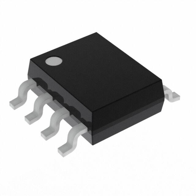


 工商网监
湘ICP备2023018690号
工商网监
湘ICP备2023018690号
