MLX90371GDC-BCC-300-SP 数据手册
MLX90371 – Triaxis® Position Processor
Datasheet
Features and Benefits
Hall Technology
On-Chip Signal Processing for Robust Absolute
Position Sensing
ISO26262
ASIL-B Safety Element out-of-Context
Programmable Measurement Range
Programmable Linear Transfer Characteristic
(Multi-points 4 or 8 points or Piece-WiseLinear 16 or 32 segments)
Selectable Analog (Ratiometric) or PWM
Output
12 bit Resolution - 10 bit Thermal Accuracy
48 bit ID Number option
Robustness against Stray-Field
Description
The MLX90371 is a monolithic sensor sensitive to
the three components of the flux density applied
to the IC (i.e. BX, BY and BZ). This allows the
MLX90371 with the correct magnetic circuit to
decode the absolute position of any magnet
moving in its vicinity (e.g. rotary position from 0
to 360 Degrees or linear displacement, see
Figure 2).
The MLX90371 reports a programmable
ratiometric analog output signal compatible with
any resistive potentiometer or programmable
linear Hall sensor. Through programming, the
MLX90371 can provide a digital PWM (Pulse
Width Modulation) output characteristic.
TEST
INPUT
Test Access
VDD
VDEC
Regulator
Rev. Pol &
Overvolt Prot.
DSP
RAM
G
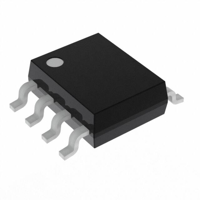
SOIC-8
TSSOP-16
DMP-4
Application Examples
Absolute Rotary Position Sensor
Absolute Linear Position Sensor
Pedal Position Sensor
Throttle Position Sensor
Ride Height Position Sensor
Steering Wheel Position Sensor
Float-Level Sensor
Non-Contacting Potentiometer
MUX
Tria xis®
VX
VY
VZ
ADC
NVRAM
Output Stage
12 bit Analog
OUT
Processor
12 bit PWM
Temp
Sensor
ROM - Firmware
VSS
�MLX90371 - Triaxis® Position Processor
Datasheet
Ordering Information
Temperature
Package
Option Code
Packing
Form
MLX90371
G
DC
BCC-100
RE
Rotary Stray-Field Immune Mode
MLX90371
G
DC
BCC-200
RE
Linear Stray-Field Immune Mode
MLX90371
G
DC
BCC-300
RE
Standard / Legacy Mode
MLX90371
G
GO
BCC-100
RE
Rotary Stray-Field Immune Mode – LowField Variant
MLX90371
G
GO
BCC-200
RE
Linear Stray-Field Immune Mode
MLX90371
G
GO
BCC-300
RE
Standard / Legacy Mode
MLX90371
G
GO
BCC-500
RE
Rotary Stray-Field Immune Mode – HighField Variant
MLX90371
G
VS
BCC-100
RE/RX
Rotary Stray-Field Immune Mode
MLX90371
G
VS
BCC-150
RE/RX
Rotary Stray-Field Immune Mode
MLX90371
G
VS
BCC-101
RE/RX
Rotary Stray-Field Immune Mode
MLX90371
G
VS
BCC-151
RE/RX
Rotary Stray-Field Immune Mode
MLX90371
G
VS
BCC-103
RE/RX
Rotary Stray-Field Immune Mode
MLX90371
G
VS
BCC-153
RE/RX
Rotary Stray-Field Immune Mode
MLX90371
G
VS
BCC-108
RE/RX
Rotary Stray-Field Immune Mode
MLX90371
G
VS
BCC-158
RE/RX
Rotary Stray-Field Immune Mode
MLX90371
G
VS
BCC-200
RE/RX
Linear Stray-Field Immune Mode
MLX90371
G
VS
BCC-250
RE/RX
Linear Stray-Field Immune Mode
MLX90371
G
VS
BCC-201
RE/RX
Linear Stray-Field Immune Mode
MLX90371
G
VS
BCC-251
RE/RX
Linear Stray-Field Immune Mode
MLX90371
G
VS
BCC-203
RE/RX
Linear Stray-Field Immune Mode
MLX90371
G
VS
BCC-253
RE/RX
Linear Stray-Field Immune Mode
MLX90371
G
VS
BCC-208
RE/RX
Linear Stray-Field Immune Mode
MLX90371
G
VS
BCC-258
RE/RX
Linear Stray-Field Immune Mode
MLX90371
G
VS
BCC-300
RE/RX
Standard / Legacy Mode
MLX90371
G
VS
BCC-350
RE/RX
Standard / Legacy Mode
MLX90371
G
VS
BCC-301
RE/RX
Standard / Legacy Mode
Product
Revision 004
Mar-19
Definition
Page 2 of 68
�MLX90371 - Triaxis® Position Processor
Datasheet
Temperature
Package
Option Code
Packing
Form
Definition
MLX90371
G
VS
BCC-351
RE/RX
Standard / Legacy Mode
MLX90371
G
VS
BCC-303
RE/RX
Standard / Legacy Mode
MLX90371
G
VS
BCC-353
RE/RX
Standard / Legacy Mode
MLX90371
G
VS
BCC-308
RE/RX
Standard / Legacy Mode
MLX90371
G
VS
BCC-358
RE/RX
Standard / Legacy Mode
Product
Revision 004
Mar-19
Page 3 of 68
�MLX90371 - Triaxis® Position Processor
Datasheet
Legend:
Temperature Code:
G: from -40°C to 160°C
Package Code:
“DC” for SOIC-8 package
“GO” for TSSOP-16 package (dual die)
“VS” for DMP-4 package (dual mold, PCB-less)
Option Code:
BCC-xxx: die Version
xxx-123:
1: Application – Magnetic configuration
1: Rotary Stray-Field Immune mode – Low-Field Variant
2: Linear Stray-Field Immune mode
3: Standard / Legacy mode (legacy backwards comparable to previous
generation)
5: Rotary Stray-Field Immune mode – High-Field Variant
2: Configuration for DMP package
0: 100nF output capacitor
5: 10nF output capacitor
3: Trim-and-Form for DMP-4
Packing Form:
0: Standard straight leads. See section 18.3.1
1: Trim-and-Form STD1 2.54. See section 18.3.2 (not recommended
for new designs, prefer STD4 2.54)
3: Trim-and-Form STD2 2.54. See section 18.3.3
8: Trim-and-Form STD4 2.54. See section 18.3.4
-RE : Tape & Reel
VS:2500 pcs/reel
DC:3000 pcs/reel
GO:4500 pcs/reel
-RX : Tape & Reel, similar to RE with parts face-down (VS package only)
Ordering Example:
“MLX90371GDC-BCC-100-RE”
For a Rotary Stray-Field Immune mode variant1 application in SOIC-8 package,
delivered in Reel.
Table 1 – Ordering information legend
Revision 004
Mar-19
Page 4 of 68
�MLX90371 - Triaxis® Position Processor
Datasheet
Contents
Features and Benefits................................................................................................................................ 1
Application Examples ................................................................................................................................ 1
Description ................................................................................................................................................ 1
Ordering Information ................................................................................................................................ 2
1. Functional Diagram ............................................................................................................................... 8
2. Glossary of Terms .................................................................................................................................. 9
3. Pin Definitions ..................................................................................................................................... 10
3.1. Pin Definition for SOIC-8 package .................................................................................................... 10
3.2. Pin Definition for TSSOP-16 package ............................................................................................... 11
3.3. Pin Definition for DMP-4 package .................................................................................................... 11
4. Absolute Maximum Ratings ................................................................................................................. 12
5. Isolation Specification.......................................................................................................................... 12
6. General Electrical Specifications .......................................................................................................... 13
7. Timing Specification............................................................................................................................. 15
7.1. General Timing .................................................................................................................................. 15
7.2. Latency Time Definition .................................................................................................................... 15
7.3. Step Response Definition ................................................................................................................. 16
7.4. Analog timing .................................................................................................................................... 16
7.5. Digital (PWM) timing ........................................................................................................................ 17
8. Magnetic Field Requirements .............................................................................................................. 18
8.1. Rotary Stray-Field Immune Mode – Low-Field Variant ................................................................... 18
8.2. Rotary Stray-Field Immune Mode – High-Field Variant .................................................................. 19
8.3. Linear Stray-Field Immune Mode .................................................................................................... 20
8.4. Standard/Legacy Mode .................................................................................................................... 22
9. Accuracy Specification ......................................................................................................................... 24
9.1. Magnetic Specification ..................................................................................................................... 24
9.1.1. Definition ..................................................................................................................................... 24
9.1.2. Rotary Stray-Field Immune Mode – Low-Field Variant............................................................. 25
9.1.3. Rotary Stray-Field Immune Mode – High-Field Variant ............................................................ 25
9.1.4. Linear Stray-Field Immune Mode .............................................................................................. 26
9.1.5. Standard/Legacy Mode .............................................................................................................. 27
Revision 004
Mar-19
Page 5 of 68
�MLX90371 - Triaxis® Position Processor
Datasheet
9.2. Analog Output Accuracy ................................................................................................................... 28
9.3. Digital (PWM) Output Accuracy ....................................................................................................... 28
9.3.1. Definition ..................................................................................................................................... 28
9.3.2. Performances .............................................................................................................................. 29
10. Memory Specification........................................................................................................................ 29
11. End-User Programmable Items.......................................................................................................... 30
12. End-User Identification Items ............................................................................................................ 33
13. Description of End-User Programmable Items................................................................................... 34
13.1. Output modes ................................................................................................................................. 34
13.1.1. OUT modes ............................................................................................................................... 34
13.1.2. PWM Output Mode .................................................................................................................. 34
13.2. Output transfer characteristic ....................................................................................................... 35
13.2.1. Enable scaling Parameter (USEROPTION_SCALING) ............................................................... 36
13.2.2. CLOCKWISE Parameter (CW) ................................................................................................... 36
13.2.3. Discontinuity Point or Zero Degree Point (DP)........................................................................ 36
13.2.4. 4-Pts LNR Parameters ............................................................................................................... 36
13.2.5. 8-Pts LNR Parameters ............................................................................................................... 37
13.2.6. 17-Pts LNR Parameters ............................................................................................................. 38
13.2.7. 32-Pts LNR Parameters ............................................................................................................. 39
13.2.8. CLAMPING Parameters............................................................................................................. 40
13.3. Sensor Front-End ............................................................................................................................ 40
13.3.1. SENSING MODE......................................................................................................................... 40
13.3.2. GAINMIN and GAINMAX Parameters ...................................................................................... 40
13.4. Filter ................................................................................................................................................ 41
13.4.1. FIR Filters ................................................................................................................................... 41
13.4.2. Exponential Moving Average Filter .......................................................................................... 42
13.5. Programmable Diagnostic Settings ................................................................................................ 42
13.5.1. DIAG mode ................................................................................................................................ 42
13.5.2. DIAG Level ................................................................................................................................. 42
13.5.3. PWM Diagnostic ....................................................................................................................... 43
13.5.4. DIAG Debouncing...................................................................................................................... 43
14. Functional Safety ............................................................................................................................... 45
14.1. Safety Mechanism .......................................................................................................................... 45
Revision 004
Mar-19
Page 6 of 68
�MLX90371 - Triaxis® Position Processor
Datasheet
14.2. Safety Manual ................................................................................................................................. 47
15. Recommended Application Diagrams ................................................................................................ 48
15.1. Wiring with the MLX90371 in SOIC-8 Package.............................................................................. 48
15.2. Wiring with the MLX90371 in TSSOP-16 Package ......................................................................... 50
15.3. Wiring with the MLX90371 in DMP-4 Package (built-in capacitors) ............................................ 52
16. Standard Information Regarding Manufacturability of Melexis Products with Different Soldering
Processes ............................................................................................................................................ 53
17. ESD Precautions................................................................................................................................. 53
18. Package Information.......................................................................................................................... 54
18.1. SOIC-8 Package ............................................................................................................................... 54
18.1.1. SOIC-8 - Package Dimensions................................................................................................... 54
18.1.2. SOIC-8 - Pinout and Marking .................................................................................................... 55
18.1.3. SOIC-8 - Sensitive Spot Positioning .......................................................................................... 55
18.1.4. SOIC-8 - Angle Detection .......................................................................................................... 56
18.2. TSSOP-16 Package .......................................................................................................................... 57
18.2.1. TSSOP-16 - Package Dimensions .............................................................................................. 57
18.2.2. TSSOP-16 - Pinout and Marking ............................................................................................... 58
18.2.3. TSSOP-16 - Sensitive Spot Positioning ..................................................................................... 58
18.2.4. TSSOP-16 - Angle detection ..................................................................................................... 60
18.3. DMP-4 Package ............................................................................................................................... 61
18.3.1. DMP-4 - Package Outline Dimensions (POD) – Straight Leads ............................................... 61
18.3.2. DMP-4 - Package Outline Dimensions (POD) – STD1 2.54 ..................................................... 62
18.3.3. DMP-4 - Package Outline Dimensions (POD) – STD2 2.54 ..................................................... 63
18.3.4. DMP-4 - Package Outline Dimensions (POD) – STD4 2.54 ..................................................... 64
18.3.5. DMP-4 - Pinout and Marking ................................................................................................... 65
18.3.6. DMP-4 - Sensitive Spot Positioning & Sense direction ........................................................... 65
18.3.7. DMP-4 - Angle detection .......................................................................................................... 67
19. Contact .............................................................................................................................................. 68
20. Disclaimer .......................................................................................................................................... 68
Revision 004
Mar-19
Page 7 of 68
�MLX90371 - Triaxis® Position Processor
Datasheet
1. Functional Diagram
INPUT
TEST
Test Access
VDD
VDEC
Regulator
Rev. Pol &
Overvolt Prot.
DSP
VX
VY
VZ
RAM
G
MUX
Tria xis®
NVRAM
Output Stage
12 bit Analog
ADC
OUT
Processor
12 bit PWM
Temp
Sensor
ROM - Firmware
VSS
Figure 1 – MLX90371 Block Diagram
Revision 004
Mar-19
Page 8 of 68
�MLX90371 - Triaxis® Position Processor
Datasheet
2. Glossary of Terms
Term
Description
Term
Description
Gauss (G),
Tesla (T)
Units for the magnetic flux density:
1 mT = 10 G
SEooC
Safety Element Out of Context
TC
Temperature Coefficient
(in ppm/Deg.C.)
FIR
Finite Impulse Response
PWM
Pulse Width Modulation
DCT
Diagnostic Cycle Time
%DC
Duty Cycle of the output signal.
i.e. TON /(TON + TOFF)
PWL
Piece Wise Linear
ADC
Analog-to-Digital Converter
IWD
Intelligent Watchdog
DAC
Digital-to-Analog Converter
AWD
Absolute Watchdog
LSB
Least Significant Bit
CPU
Central Processing Unit
MSB
Most Significant Bit
POR
Power On Reset
DNL
Differential Non-Linearity
SW
Software
INL
Integral Non-Linearity
HW
Hardware
ASP
Analog Signal Processing
ECC
Error-Correcting Code
DSP
Digital Signal Processing
ROM
Read-only Memory
EMC
Electro-Magnetic Compatibility
RAM
Random-access Memory
DMP
Dual Mold Package
NVRAM
Non-volatile Random-access Memory
DP
Discontinuity Point
AoU
Assumptions of Use
EoL
End of Line
IMC
Integrated Magnetic Concentrator
Table 2 – Glossary of Terms
Revision 004
Mar-19
Page 9 of 68
�MLX90371 - Triaxis® Position Processor
Datasheet
3. Pin Definitions
3.1. Pin Definition for SOIC-8 package
Pin #
Name
Description
1
VDD
Supply
2
Test Input
For test
3
Test
For test
4
Not Used
5
OUT
Output
6
VSSD
Ground
7
VDEC
Decoupling pin (on-chip regulator)
8
VSSA
Ground
Table 3 – SOIC-8 Pin Definitions and Descriptions
For optimal EMC behavior, it is recommended to connect the unused pins (Not Used and Test) to the Ground
(see section 15.1).
Revision 004
Mar-19
Page 10 of 68
�MLX90371 - Triaxis® Position Processor
Datasheet
3.2. Pin Definition for TSSOP-16 package
Pin #
Name
Description
1
VDEC1
Decoupling pin
2
VSSA1
Ground
3
VDD1
Supply
4
Test Input1
For test
5
Test2
For test
6
OUT2
Output
7
Not Used2
8
VSSD2
Ground
9
VDEC2
Decoupling pin
10
VSSA2
Ground
11
VDD2
Supply
12
Test Input2
For test
13
Test1
For test
14
Not Used1
15
OUT1
Output
16
VSSD1
Ground
Table 4 – TSSOP-16 Pin Definitions and Descriptions
For optimal EMC behavior, it is recommended to connect the unused pins (Not Used and Test) to the Ground
(see section 15.2).
3.3. Pin Definition for DMP-4 package
Pin #
Name
Description
1
VSS
Ground
2
VDD
Supply
3
OUT
Output
4
VSS
Ground
Table 5 – DMP-4 Pin Definitions and Descriptions
Revision 004
Mar-19
Page 11 of 68
�MLX90371 - Triaxis® Position Processor
Datasheet
4. Absolute Maximum Ratings
Parameter
Supply Voltage
Symbol
Min.
Typ.
VDD
Reverse Voltage Protection
VDDREV
Positive Output Voltage
VOUT
Output Current
IOUT
-30
Reverse Output Voltage
VOUTREV
-0.3
Operating Temperature
TAMB
-40
Junction Temperature
TJUNC
Storage Temperature
TST
Magnetic Flux Density
Max.
Unit
28
45
V
MLX90371GDC-BCC-300-SP 价格&库存
很抱歉,暂时无法提供与“MLX90371GDC-BCC-300-SP”相匹配的价格&库存,您可以联系我们找货
免费人工找货- 国内价格 香港价格
- 3+33.457943+4.06164
- 15+33.3015915+4.04266
- 50+33.3008650+4.04257
- 150+33.30012150+4.04248
- 500+33.29938500+4.04239


 工商网监
湘ICP备2023018690号
工商网监
湘ICP备2023018690号
